EP0822590A2 - Procédé et appareil pour la libération d'une pièce d'un mandrin électrostatique - Google Patents
Procédé et appareil pour la libération d'une pièce d'un mandrin électrostatique Download PDFInfo
- Publication number
- EP0822590A2 EP0822590A2 EP97305146A EP97305146A EP0822590A2 EP 0822590 A2 EP0822590 A2 EP 0822590A2 EP 97305146 A EP97305146 A EP 97305146A EP 97305146 A EP97305146 A EP 97305146A EP 0822590 A2 EP0822590 A2 EP 0822590A2
- Authority
- EP
- European Patent Office
- Prior art keywords
- electrode
- inductor
- chuck
- wafer
- electrostatic chuck
- Prior art date
- Legal status (The legal status is an assumption and is not a legal conclusion. Google has not performed a legal analysis and makes no representation as to the accuracy of the status listed.)
- Withdrawn
Links
Images

Classifications
-
- H—ELECTRICITY
- H10—SEMICONDUCTOR DEVICES; ELECTRIC SOLID-STATE DEVICES NOT OTHERWISE PROVIDED FOR
- H10P—GENERIC PROCESSES OR APPARATUS FOR THE MANUFACTURE OR TREATMENT OF DEVICES COVERED BY CLASS H10
- H10P72/00—Handling or holding of wafers, substrates or devices during manufacture or treatment thereof
- H10P72/70—Handling or holding of wafers, substrates or devices during manufacture or treatment thereof for supporting or gripping
- H10P72/72—Handling or holding of wafers, substrates or devices during manufacture or treatment thereof for supporting or gripping using electrostatic chucks
- H10P72/722—Details of electrostatic chucks
-
- H—ELECTRICITY
- H02—GENERATION; CONVERSION OR DISTRIBUTION OF ELECTRIC POWER
- H02N—ELECTRIC MACHINES NOT OTHERWISE PROVIDED FOR
- H02N13/00—Clutches or holding devices using electrostatic attraction, e.g. using Johnson-Rahbek effect
-
- Y—GENERAL TAGGING OF NEW TECHNOLOGICAL DEVELOPMENTS; GENERAL TAGGING OF CROSS-SECTIONAL TECHNOLOGIES SPANNING OVER SEVERAL SECTIONS OF THE IPC; TECHNICAL SUBJECTS COVERED BY FORMER USPC CROSS-REFERENCE ART COLLECTIONS [XRACs] AND DIGESTS
- Y10—TECHNICAL SUBJECTS COVERED BY FORMER USPC
- Y10T—TECHNICAL SUBJECTS COVERED BY FORMER US CLASSIFICATION
- Y10T279/00—Chucks or sockets
- Y10T279/23—Chucks or sockets with magnetic or electrostatic means
Definitions
- the invention generally relates to electrostatic chucks for holding a workpiece and, more specifically, to methods and apparatus for releasing a workpiece (such as a semiconductor wafer) from an electrostatic chuck.
- Electrostatic chucks are used for holding a workpiece in various applications ranging from holding a sheet of paper in a computer graphics plotter to holding a semiconductor wafer within a semiconductor fabrication process chamber.
- electrostatic chucks vary in design, they all are based on the principle of applying a voltage to one or more electrodes in the chuck so as to induce opposite polarity charges in the workpiece and electrodes, respectively. The electrostatic attractive force between the oppositely polarized charges pulls the workpiece against the chuck, thereby retaining the workpiece.
- a problem with electrostatic chucks is the difficulty of removing the electric charge from the workpiece and the chuck when it is desired to release the workpiece from the chuck.
- One conventional solution is to connect both the electrode and the workpiece to ground to drain the charge.
- Another conventional solution which purportedly removes the charge more quickly is to reverse the polarity of the DC voltage applied to the electrodes. This technique is described in the context of a chuck having two electrodes (a bipolar chuck) in U.S. Patent 5,117,121 issued to Watanabe et al.
- the present invention is an apparatus and concomitant method that applies an oscillating voltage to the electrostatic chuck to discharge the residual charge between the wafer and chuck.
- the apparatus contains a relay connected between the electrostatic chuck power supply and an electrode of an electrostatic chuck. In a first contact position, the relay applies a chucking voltage to the electrode(s) of the electrostatic chuck. While in a second contact position, the relay disconnects the power supply from the electrode(s) and connects the electrode(s) through an inductor to ground.
- the relay is switched from the first position to the second position connecting the electrode(s) to ground.
- the residual charge will discharge from the electrode-wafer interface through the inductor to ground.
- the wafer and chuck electrode form a parallel plate capacitor having the wafer connected to ground through a plasma and the electrode connected to the inductor through the relay, this capacitor in combination with the inductor forms a resonant tank circuit that oscillates at a resonant frequency.
- energy is transferred in an oscillatory manner between the capacitor and inductor, and vice versa.
- the current between the capacitor and inductor oscillates in a decaying manner over a period of time.
- the decay rate is defined by the Q of the tank circuit. This oscillatory energy transfer discharges any residual charge that is trapped between the wafer and the chuck electrode.
- the method of discharging the residual charge includes the steps of: disconnecting the electrostatic chuck from the chucking voltage; connecting the electrode (or electrodes) of the electrostatic chuck through the inductor to ground; and, shortly after making this confection, disconnecting the power to the plasma within the reaction chamber.
- the tank circuit oscillates at a resonant frequency and repetitively applies a positive and negative voltage to the wafer and chuck surface interface. Consequently, the charge trapped at the interface dissipates quickly as the tank circuit oscillations decay. Since there is no external energy used to discharge the surface of the electrostatic chuck, the method of the present invention is said to be "self-sweeping".
- Empirical evidence indicates that a monopolar chuck retaining a wafer with a chucking voltage of 1200 volts can be discharged in approximately 8 msec. To achieve such rapid discharge a 5.4 mH inductor was used.
- FIG. 1 depicts such a monopolar chuck 110 as typically would be configured within a vacuum chamber 100 used for plasma enhanced processing (e.g., etching or chemical vapor deposition) of a semiconductor wafer 101.
- plasma enhanced processing e.g., etching or chemical vapor deposition
- the conventional vacuum chamber 100 includes a vacuum tight enclosure 105 which is made of aluminum and is electrically grounded.
- a disk-shaped anodized aluminum anode electrode 104 is mounted just below the upper wall or lid of the enclosure 105 and is electrically connected to the grounded enclosure.
- the walls of the grounded enclosure form the anode electrode.
- the enclosure forms the cathode electrode (the powered electrode) while the chuck forms the anode electrode (grounded electrode).
- the conventional monopolar electrostatic chuck includes an anodized solid aluminum cathode pedestal 111 having a circular, planar top face; a lower dielectric layer 112 bonded to the top surface of the pedestal; a metal chuck electrode 113 bonded to the top surface of the lower dielectric; and an upper dielectric layer 114 bonded to the top face of the chuck electrode.
- each dielectric layer is an approximately 75 micron thick layer of polyimide.
- the cathode pedestal 111 is mounted on top of and electrically connected to a hollow anodized aluminum cathode base 135.
- the cathode base is mounted on the lower wall of enclosure 105 by means of an electrically insulating annular flange 147.
- Electrical connection to the cathode is made by a copper rod 138 having a threaded end which is screwed into a tapped hole at the bottom of the cathode base 135.
- a copper clip (not shown) connects the rod 138 to RF transmission line 134, which in turn connects to an RF matching network 132, which in turn connects to RF power supply 130.
- Electrical connection to the chuck electrode 113 is made by an insulated wire 122 which is attached to the chuck electrode 113 at point 115.
- the wire 122 extends downward from the electrode 113 through a bore 125 in the cathode pedestal 111, and then out the bottom of the enclosure 105 through a feed-through insulator 124.
- the wire 122 connects to a common terminal (C) of a relay 210.
- the normally open terminal (NO) of the relay connects to an RF blocking low pass filter 121, and in turn, to DC voltage supply 120.
- the normally closed terminal (NC) of the relay connects to one terminal of an inductor 212.
- the other terminal of the inductor 212 connects to a predetermined potential (e.g., ground).
- an inductor 222 can be connected in wire 122, i.e., connected between the common terminal (c) of the relay 210 and the electrode 113.
- the normally closed terminal of the relay is then connected to the predetermined potential (e.g., ground). Both embodiments function in the same manner to discharge the residual charge from the chuck.
- a robot arm removes the wafer from the chamber.
- several (preferably four, but at least three) lift pins 142 lift the wafer 2 to 5 centimeters about the chuck 110.
- Each lift pin 142 slides vertically in a corresponding bore 144 in the cathode pedestal 111. All the lift pins 142 are mounted on a carriage 140, which is raised and lower by a pneumatic lift mechanism 146 under control of a programmable digital computer 200.
- the lift pins 142 and carriage 140 are considered inside the cathode base 135 within the vacuum chamber 100, whereas the pneumatic lift mechanism 146 is outside the vacuum chamber. They are mechanically connected by a linkage 149 passing through a bellows 143 which permits vertical movement while maintaining a vacuum seal.
- a robot arm moves a wafer 101 into the chamber through a slit valve 106.
- the robot places the wafer on the tips of lift pins 142, which at this time are elevated by the pneumatic lift mechanism 146 so as to protrude 2 to 5 centimeters above the top of the electrostatic chuck 110.
- the pneumatic mechanism then lowers the lift pins 142 so that the wafer 101 drops onto the top face of the chuck 110, the wafer's descent time typically is 3 to 10 seconds.
- the plasma gas flows into the chamber, the RF power supply applies RF power to the cathode pedestal, and the plasma is ignited within the space between the wafer 101 and the anode 104.
- the plasma forms a conductive path from the wafer to ground.
- a DC voltage drop appears across the plasma so that the wafer is negatively biased relative to the grounded enclosure 105. If the chucking voltage applied to the chuck electrode 113 by the DC voltage supply 120 is positive, the total voltage between the wafer and the chuck electrode will be the sum of the wafer bias voltage and the chucking power supply voltage.
- the wafer bias increases the electrostatic force retaining the wafer.
- the relay 210 is energized to place the relay contacts in the open position.
- the chuck voltage supply 120 applies a high DC voltage, on the order of plus 1200 volts, to the chuck electrode 113 relative to ground as illustrated on the left side of the graph of FIG. 2.
- This voltage causes negative and positive charges to accumulate on the facing surfaces of the wafer and chuck electrode, respectively.
- the amount of charge is proportional to the product of the voltage and the capacitance between the wafer and the chuck electrode.
- the opposite polarity charges on the wafer and the chuck electrode produce an electrostatic attractive force which pulls the wafer against the upper face of the chuck.
- the chucking voltage (1200 volts in this example) is set to a value high enough to produce an electrostatic force between the wafer and the chuck adequate to prevent wafer movement during subsequent process steps.
- the wafer thus retained securely on the chuck is said to be "chucked.”
- one or more semiconductor fabrication process steps are performed in the chamber 100, such as deposition or etching of films on the wafer. Additionally, once the wafer is chucked, a backside coolant such as helium can be applied between the wafer and chuck surface to promote heat conduction from the wafer to the pedestal.
- a backside coolant such as helium can be applied between the wafer and chuck surface to promote heat conduction from the wafer to the pedestal.
- the backside coolant is removed and the pneumatic lift mechanism 146 raises the lift pins 142 to raise the wafer above the chuck 110 so that the wafer can be removed from the chamber by a robot.
- the wafer must be "dechucked”; that is, the electrostatic force retaining the wafer on the chuck 100 must be removed.
- the electrostatic force on the wafer can be essentially eliminated, thereby permitting easy removal of the wafer from the chuck.
- the method of the present invention applies an oscillating voltage to the wafer chuck interface which, over a short period of time, discharges the residual charge that has accumulated between the wafer and the chuck.
- the apparatus of the present invention comprises the relay 210 connected between the electrostatic chuck electrode 113 and the electrostatic chuck power supply 120.
- the normally closed position (NC) of the relay 210 connects the chuck electrode 113 to ground through the inductor 212.
- This inductor has an inductance between 1 and 10 mH.
- the normally open position (NO) of the relay 210 connects the power supply 120 to the electrostatic chuck electrode 113.
- the relay is positioned in the normally open position such that the power supply is connected to the electrostatic chuck electrode, i.e., the relay coil is powered by the control computer 200 to position the contacts in the normally open position.
- the relay When dechucking is required, the relay is switched into the normally closed position, i.e., the control computer disconnects power from the relay coil, and the relay connects the chuck electrode 113 to the inductor 212. Initially, when the electrode is connected to the inductor, the plasma remains energized in the chamber, effectively connecting the wafer through the plasma to the top electrode or any grounded surface in the chamber. As such, while the plasma is maintained, the wafer and chuck electrode form a parallel plate capacitor that is connected in parallel with the inductor.
- This dechucking apparatus forms an LC tank circuit comprising the inductor 212 and the capacitor formed between the wafer 101 and the chuck electrode 113.
- the tank circuit has a resonant frequency of 2 ⁇ (LC) 1/2 .
- the voltage within the tank circuit oscillates at the resonant frequency for a period of time that is defined by the Q of the LC circuit.
- the computer 200 disables the RF power maintaining the plasma, and the plasma is de-energized.
- the amount of time for retaining the plasma after disconnecting the chucking voltage from the electrostatic chuck is approximately one second.
- the duration is defined by the decay time of the tank circuit, e.g., the plasma is discontinued after substantially all the residual charge is removed from the chuck surface.
- the wafer and the upper dielectric both have, at a microscopic level, imperfectly flat surfaces, the wafer and the dielectric actually contact each other only at thousands of tiny points, leaving thousands of microscopic gaps between the wafer and the dielectric.
- the chucking voltage between the wafer and the chuck electrode produces a strong electric field across these microscopic gaps.
- this electric field causes electrons to migrate from the wafer to the adjacent surface of the upper dielectric through the physical mechanism of field emission.
- the chucking voltage, and hence the electric field is removed, the electrons accumulated in the dielectric have no discharge path, so they remain in the dielectric.
- the electrons are given a discharge path through the inductor, however, because of the parallel plate capacitance of the wafer and chuck electrode combination, the voltage within the inductor-capacitor combination oscillates in a positive and negative manner until the energy within the circuit has been dissipated. This oscillating voltage discharges the residual charge without applying any external voltage to the chuck electrode.
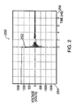
- FIG. 2 depicts a graph 250 of the oscillating voltage 252 as measured on the electrode of the electrostatic chuck during discharge of the residual charge between the wafer and the electrostatic chuck.
- the vertical axis 254 represent voltage and the horizontal axis 256 represents time in milliseconds.
- This data was measured in a Model 5300 high density oxide etch wafer processing system manufactured by Applied Materials, Inc. of Santa Clara, California.
- the discharge inductor had a value of 5.4 mH and the inventive method discussed above was used to dissipate the residual charge between the wafer and chuck.
- the voltage is discharged from approximately 1,200 volts (the chucking voltage) to 0 volts within approximately 8 milliseconds.
- the resonant frequency of this exemplary circuit is approximately 5 kHz.
- the inventive apparatus can be adapted for use in other types of electrostatic chucks such as bipolar chucks by providing a relay and inductor for each electrode of the chuck. As such, during dechucking, a pair of resonant LC circuits are produced to discharge any residual charge between the electrodes and the workpiece.
- the chucking voltage is a positive voltage that causes electrons to accumulate on the surface of the chuck. It should be understood that in some applications of electrostatic chucks, for example, ceramic chucks used in high density plasma applications, the chucking voltage is a negative voltage that causes positive charge to accumulate on the surface of the chuck. Although the polarity is reversed, the dechucking apparatus and method are the same as discussed above.
- some plasma reactors do not apply RF power to the pedestal or, alternatively, may supplement the RF power applied to the pedestal, by applying RF power to an antenna (coils) that circumscribes the reaction chamber.
- the dechucking method requires maintaining the connection of RF power to the antenna when the chucking voltage is disconnected. As such, the plasma is maintained while the residual charge is removed by the invention.
- the foregoing disclosure used the plasma within the chamber to form a conductive path from the wafer to ground.
- this path is available only in processing systems that use a plasma. Therefore, in systems that do not use a plasma or systems that require termination of the plasma prior to dechucking, the conductive path can be provided using a physical conductor.
- a conductive trace can be affixed to the support surface of the electrostatic chuck such that the underside of the wafer contacts the trace. To dechuck the wafer, the trace is connected to ground when the relay is switched to connect the inductor to the electrode.
- a double pole, double throw relay could be used to accomplish the simultaneous switching function.
Landscapes
- Container, Conveyance, Adherence, Positioning, Of Wafer (AREA)
- Jigs For Machine Tools (AREA)
- Electrical Discharge Machining, Electrochemical Machining, And Combined Machining (AREA)
Applications Claiming Priority (2)
| Application Number | Priority Date | Filing Date | Title |
|---|---|---|---|
| US690086 | 1996-07-31 | ||
| US08/690,086 US5790365A (en) | 1996-07-31 | 1996-07-31 | Method and apparatus for releasing a workpiece from and electrostatic chuck |
Publications (2)
| Publication Number | Publication Date |
|---|---|
| EP0822590A2 true EP0822590A2 (fr) | 1998-02-04 |
| EP0822590A3 EP0822590A3 (fr) | 1999-10-13 |
Family
ID=24771021
Family Applications (1)
| Application Number | Title | Priority Date | Filing Date |
|---|---|---|---|
| EP97305146A Withdrawn EP0822590A3 (fr) | 1996-07-31 | 1997-07-11 | Procédé et appareil pour la libération d'une pièce d'un mandrin électrostatique |
Country Status (5)
| Country | Link |
|---|---|
| US (1) | US5790365A (fr) |
| EP (1) | EP0822590A3 (fr) |
| JP (1) | JPH1074826A (fr) |
| KR (1) | KR980012817A (fr) |
| TW (1) | TW328613B (fr) |
Cited By (10)
| Publication number | Priority date | Publication date | Assignee | Title |
|---|---|---|---|---|
| US6307728B1 (en) | 2000-01-21 | 2001-10-23 | Applied Materials, Inc. | Method and apparatus for dechucking a workpiece from an electrostatic chuck |
| EP1096561A3 (fr) * | 1999-10-08 | 2002-04-17 | Applied Materials, Inc. | Méthode permettant d'enlever rapidement une plaquette semi-conductrice d'un mandrin électrostatique |
| EP1286391A1 (fr) * | 2001-08-13 | 2003-02-26 | Nissin Electric Co., Ltd. | Appareil et procédé de serrage un substrat |
| WO2002078062A3 (fr) * | 2001-03-27 | 2003-03-13 | Lam Res Corp | Detection acoustique de separation et dispositif associe |
| EP1047125A3 (fr) * | 1999-04-19 | 2004-01-21 | Applied Materials, Inc. | Procédé permettant d'enlever rapidement d'un mandrin électrostatique des plaquettes semi-conductrice en utiliser un cycle hystérèse |
| US7055935B2 (en) | 1997-07-15 | 2006-06-06 | Silverbrook Research Pty Ltd | Ink ejection devices within an inkjet printer |
| US7147305B2 (en) | 1997-07-15 | 2006-12-12 | Silverbrook Research Pty Ltd | Printer formed from integrated circuit printhead |
| US7246884B2 (en) | 1997-07-15 | 2007-07-24 | Silverbrook Research Pty Ltd | Inkjet printhead having enclosed inkjet actuators |
| US7278711B2 (en) | 1997-07-15 | 2007-10-09 | Silverbrook Research Pty Ltd | Nozzle arrangement incorporating a lever based ink displacement mechanism |
| US7556356B1 (en) | 1997-07-15 | 2009-07-07 | Silverbrook Research Pty Ltd | Inkjet printhead integrated circuit with ink spread prevention |
Families Citing this family (42)
| Publication number | Priority date | Publication date | Assignee | Title |
|---|---|---|---|---|
| US5997962A (en) * | 1995-06-30 | 1999-12-07 | Tokyo Electron Limited | Plasma process utilizing an electrostatic chuck |
| JP3245369B2 (ja) * | 1996-11-20 | 2002-01-15 | 東京エレクトロン株式会社 | 被処理体を静電チャックから離脱する方法及びプラズマ処理装置 |
| US6177023B1 (en) * | 1997-07-11 | 2001-01-23 | Applied Komatsu Technology, Inc. | Method and apparatus for electrostatically maintaining substrate flatness |
| US6057244A (en) * | 1998-07-31 | 2000-05-02 | Applied Materials, Inc. | Method for improved sputter etch processing |
| US6221221B1 (en) | 1998-11-16 | 2001-04-24 | Applied Materials, Inc. | Apparatus for providing RF return current path control in a semiconductor wafer processing system |
| US6821571B2 (en) | 1999-06-18 | 2004-11-23 | Applied Materials Inc. | Plasma treatment to enhance adhesion and to minimize oxidation of carbon-containing layers |
| JP3464177B2 (ja) * | 1999-09-06 | 2003-11-05 | 沖電気工業株式会社 | 半導体製造装置および静電気除去方法 |
| US6676800B1 (en) * | 2000-03-15 | 2004-01-13 | Applied Materials, Inc. | Particle contamination cleaning from substrates using plasmas, reactive gases, and mechanical agitation |
| US6794311B2 (en) | 2000-07-14 | 2004-09-21 | Applied Materials Inc. | Method and apparatus for treating low k dielectric layers to reduce diffusion |
| JP4559595B2 (ja) * | 2000-07-17 | 2010-10-06 | 東京エレクトロン株式会社 | 被処理体の載置装置及びプラズマ処理装置 |
| KR100376879B1 (ko) * | 2000-11-01 | 2003-03-19 | 주식회사 하이닉스반도체 | 스틱킹이 없는 정전척 |
| JP2002203837A (ja) * | 2000-12-28 | 2002-07-19 | Mitsubishi Electric Corp | プラズマ処理方法および装置並びに半導体装置の製造方法 |
| US6962879B2 (en) * | 2001-03-30 | 2005-11-08 | Lam Research Corporation | Method of plasma etching silicon nitride |
| US6665168B2 (en) | 2001-03-30 | 2003-12-16 | Taiwan Semiconductor Manufacturing Co. Ltd | Electrostatic chuck apparatus and method for efficiently dechucking a substrate therefrom |
| US8361340B2 (en) * | 2003-04-28 | 2013-01-29 | Air Products And Chemicals, Inc. | Removal of surface oxides by electron attachment |
| US7387738B2 (en) | 2003-04-28 | 2008-06-17 | Air Products And Chemicals, Inc. | Removal of surface oxides by electron attachment for wafer bumping applications |
| US7897029B2 (en) * | 2008-03-04 | 2011-03-01 | Air Products And Chemicals, Inc. | Removal of surface oxides by electron attachment |
| US7198276B2 (en) * | 2003-10-24 | 2007-04-03 | International Business Machines Corporation | Adaptive electrostatic pin chuck |
| US7534301B2 (en) * | 2004-09-21 | 2009-05-19 | Applied Materials, Inc. | RF grounding of cathode in process chamber |
| US7511936B2 (en) * | 2005-07-20 | 2009-03-31 | Taiwan Semiconductor Manufacturing Co., Ltd. | Method and apparatus for dynamic plasma treatment of bipolar ESC system |
| JP5094002B2 (ja) * | 2005-09-06 | 2012-12-12 | ルネサスエレクトロニクス株式会社 | プラズマ処理装置およびその異常放電抑止方法 |
| KR100819078B1 (ko) * | 2006-11-27 | 2008-04-02 | 삼성전자주식회사 | 정전 척에서 웨이퍼를 디척킹하는 장치 및 방법 |
| KR101312292B1 (ko) * | 2006-12-11 | 2013-09-27 | 엘아이지에이디피 주식회사 | 플라즈마 처리장치의 기판 파손 방지장치 및 그 방법 |
| US7508494B2 (en) * | 2006-12-22 | 2009-03-24 | Asml Netherlands B.V. | Lithographic apparatus and a subtrate table for exciting a shockwave in a substrate |
| US8149562B2 (en) * | 2007-03-09 | 2012-04-03 | Taiwan Semiconductor Manufacturing Company, Ltd. | System for decharging a wafer or substrate after dechucking from an electrostatic chuck |
| KR101295776B1 (ko) * | 2007-08-02 | 2013-08-12 | 삼성전자주식회사 | 직류 및 교류 전압들을 교대로 사용하는 웨이퍼의 디척킹방법 및 이를 채택하는 반도체 소자의 제조 장치 |
| US7995323B2 (en) * | 2008-07-14 | 2011-08-09 | Taiwan Semiconductor Manufacturing Co., Ltd. | Method and apparatus for securely dechucking wafers |
| US8416555B2 (en) | 2008-07-14 | 2013-04-09 | Taiwan Semiconductor Manufacturing Co., Ltd. | System for securely dechucking wafers |
| US8000081B2 (en) * | 2008-07-14 | 2011-08-16 | Taiwan Semiconductor Manufacturing Co., Ltd. | Method and apparatus for safely dechucking wafers |
| CN101872733B (zh) * | 2009-04-24 | 2012-06-27 | 中微半导体设备(上海)有限公司 | 感测和移除被加工半导体工艺件的残余电荷的系统和方法 |
| CN102044466B (zh) * | 2009-10-12 | 2013-03-27 | 北京北方微电子基地设备工艺研究中心有限责任公司 | 一种静电卡盘及其残余电荷的消除方法 |
| US9666466B2 (en) * | 2013-05-07 | 2017-05-30 | Applied Materials, Inc. | Electrostatic chuck having thermally isolated zones with minimal crosstalk |
| US9232626B2 (en) | 2013-11-04 | 2016-01-05 | Kla-Tencor Corporation | Wafer grounding using localized plasma source |
| WO2018162070A1 (fr) * | 2017-03-09 | 2018-09-13 | Ev Group E. Thallner Gmbh | Support de substrat électrostatique |
| CN110581099B (zh) * | 2018-06-07 | 2022-06-14 | 北京北方华创微电子装备有限公司 | 静电卡盘和工艺腔室 |
| US11798833B2 (en) | 2020-02-26 | 2023-10-24 | Applied Materials, Inc. | Methods of use of a servo control system |
| US11415230B2 (en) | 2020-03-31 | 2022-08-16 | Applied Material, Inc. | Slit valve pneumatic control |
| JP7515327B2 (ja) * | 2020-07-13 | 2024-07-12 | 東京エレクトロン株式会社 | 基板離脱方法及びプラズマ処理装置 |
| JP7527194B2 (ja) * | 2020-12-23 | 2024-08-02 | 東京エレクトロン株式会社 | プラズマ処理装置およびプラズマ処理方法 |
| CN114695051B (zh) * | 2020-12-31 | 2025-02-21 | 拓荆科技股份有限公司 | 半导体处理设备及方法 |
| CN113862645B (zh) * | 2021-09-28 | 2023-09-08 | 北京北方华创微电子装备有限公司 | 承载装置及半导体工艺腔室 |
| CN120473429B (zh) * | 2025-07-09 | 2025-10-10 | 华通芯电(南昌)电子科技有限公司 | 一种静电吸盘及静电吸盘控制方法 |
Family Cites Families (17)
| Publication number | Priority date | Publication date | Assignee | Title |
|---|---|---|---|---|
| US3767551A (en) * | 1971-11-01 | 1973-10-23 | Varian Associates | Radio frequency sputter apparatus and method |
| JPS57149734A (en) * | 1981-03-12 | 1982-09-16 | Anelva Corp | Plasma applying working device |
| JPS6244332A (ja) * | 1985-08-23 | 1987-02-26 | Canon Inc | 静電吸着装置 |
| JPS6399148A (ja) * | 1986-10-15 | 1988-04-30 | Tokuda Seisakusho Ltd | 静電チヤツク装置 |
| JP2779950B2 (ja) * | 1989-04-25 | 1998-07-23 | 東陶機器株式会社 | 静電チャックの電圧印加方法および電圧印加装置 |
| EP0439000B1 (fr) * | 1990-01-25 | 1994-09-14 | Applied Materials, Inc. | Dispositif de serrage électrostatique et procédé |
| JP2506219B2 (ja) * | 1990-06-19 | 1996-06-12 | 富士通株式会社 | 静電吸着方法 |
| JPH06103683B2 (ja) * | 1990-08-07 | 1994-12-14 | 株式会社東芝 | 静電吸着方法 |
| US5325261A (en) * | 1991-05-17 | 1994-06-28 | Unisearch Limited | Electrostatic chuck with improved release |
| JPH05275517A (ja) * | 1992-03-30 | 1993-10-22 | Fujitsu Ltd | 基板離脱方法 |
| US5460684A (en) * | 1992-12-04 | 1995-10-24 | Tokyo Electron Limited | Stage having electrostatic chuck and plasma processing apparatus using same |
| JP3264391B2 (ja) * | 1993-05-17 | 2002-03-11 | 東京エレクトロン株式会社 | 静電吸着体の離脱装置 |
| US5542559A (en) * | 1993-02-16 | 1996-08-06 | Tokyo Electron Kabushiki Kaisha | Plasma treatment apparatus |
| US5665167A (en) * | 1993-02-16 | 1997-09-09 | Tokyo Electron Kabushiki Kaisha | Plasma treatment apparatus having a workpiece-side electrode grounding circuit |
| JPH06244270A (ja) * | 1993-02-19 | 1994-09-02 | Ulvac Japan Ltd | 静電吸着装置 |
| TW255839B (fr) * | 1993-05-20 | 1995-09-01 | Hitachi Seisakusyo Kk | |
| US5459632A (en) * | 1994-03-07 | 1995-10-17 | Applied Materials, Inc. | Releasing a workpiece from an electrostatic chuck |
-
1996
- 1996-07-31 US US08/690,086 patent/US5790365A/en not_active Expired - Lifetime
-
1997
- 1997-06-14 TW TW086108260A patent/TW328613B/zh active
- 1997-07-11 EP EP97305146A patent/EP0822590A3/fr not_active Withdrawn
- 1997-07-31 JP JP20613497A patent/JPH1074826A/ja not_active Withdrawn
- 1997-07-31 KR KR1019970036297A patent/KR980012817A/ko not_active Withdrawn
Cited By (16)
| Publication number | Priority date | Publication date | Assignee | Title |
|---|---|---|---|---|
| US7506965B2 (en) | 1997-07-15 | 2009-03-24 | Silverbrook Research Pty Ltd | Inkjet printhead integrated circuit with work transmitting structures |
| US7278711B2 (en) | 1997-07-15 | 2007-10-09 | Silverbrook Research Pty Ltd | Nozzle arrangement incorporating a lever based ink displacement mechanism |
| US7942503B2 (en) | 1997-07-15 | 2011-05-17 | Silverbrook Research Pty Ltd | Printhead with nozzle face recess to contain ink floods |
| US7866797B2 (en) | 1997-07-15 | 2011-01-11 | Silverbrook Research Pty Ltd | Inkjet printhead integrated circuit |
| US7556356B1 (en) | 1997-07-15 | 2009-07-07 | Silverbrook Research Pty Ltd | Inkjet printhead integrated circuit with ink spread prevention |
| US7055935B2 (en) | 1997-07-15 | 2006-06-06 | Silverbrook Research Pty Ltd | Ink ejection devices within an inkjet printer |
| US7147305B2 (en) | 1997-07-15 | 2006-12-12 | Silverbrook Research Pty Ltd | Printer formed from integrated circuit printhead |
| US7246884B2 (en) | 1997-07-15 | 2007-07-24 | Silverbrook Research Pty Ltd | Inkjet printhead having enclosed inkjet actuators |
| EP1047125A3 (fr) * | 1999-04-19 | 2004-01-21 | Applied Materials, Inc. | Procédé permettant d'enlever rapidement d'un mandrin électrostatique des plaquettes semi-conductrice en utiliser un cycle hystérèse |
| EP1096561A3 (fr) * | 1999-10-08 | 2002-04-17 | Applied Materials, Inc. | Méthode permettant d'enlever rapidement une plaquette semi-conductrice d'un mandrin électrostatique |
| US6307728B1 (en) | 2000-01-21 | 2001-10-23 | Applied Materials, Inc. | Method and apparatus for dechucking a workpiece from an electrostatic chuck |
| KR100830070B1 (ko) | 2001-03-27 | 2008-05-16 | 램 리써치 코포레이션 | 디척킹에 대한 음향 검출 및 그를 위한 장치 |
| US6578423B2 (en) | 2001-03-27 | 2003-06-17 | Lam Research Corporation | Acoustic detection of dechucking and apparatus therefor |
| WO2002078062A3 (fr) * | 2001-03-27 | 2003-03-13 | Lam Res Corp | Detection acoustique de separation et dispositif associe |
| US6831823B2 (en) | 2001-08-13 | 2004-12-14 | Nissin Electric Co., Ltd. | Method and apparatus for chucking a substrate |
| EP1286391A1 (fr) * | 2001-08-13 | 2003-02-26 | Nissin Electric Co., Ltd. | Appareil et procédé de serrage un substrat |
Also Published As
| Publication number | Publication date |
|---|---|
| JPH1074826A (ja) | 1998-03-17 |
| TW328613B (en) | 1998-03-21 |
| EP0822590A3 (fr) | 1999-10-13 |
| US5790365A (en) | 1998-08-04 |
| KR980012817A (ko) | 1998-04-30 |
Similar Documents
| Publication | Publication Date | Title |
|---|---|---|
| US5790365A (en) | Method and apparatus for releasing a workpiece from and electrostatic chuck | |
| US5946184A (en) | Electrostatic chuck, and method of and apparatus for processing sample | |
| US5460684A (en) | Stage having electrostatic chuck and plasma processing apparatus using same | |
| US5539179A (en) | Electrostatic chuck having a multilayer structure for attracting an object | |
| KR100378187B1 (ko) | 정전척을 구비한 웨이퍼 지지대 및 이를 이용한 웨이퍼 디척킹 방법 | |
| US6099697A (en) | Method of and apparatus for restoring a support surface in a semiconductor wafer processing system | |
| US8277673B2 (en) | Plasma processing method and apparatus | |
| KR101247712B1 (ko) | 기판을 디처킹하기 위한 방법 및 장치 | |
| JP4354983B2 (ja) | 基板処理設備 | |
| JPH03211753A (ja) | 半導体製造装置 | |
| US11495444B2 (en) | Substrate processing apparatus and substrate processing method | |
| US20240355663A1 (en) | Etching apparatus and methods of cleaning thereof | |
| US20030236004A1 (en) | Dechucking with N2/O2 plasma | |
| US6185085B1 (en) | System for transporting and electrostatically chucking a semiconductor wafer or the like | |
| US6238160B1 (en) | Method for transporting and electrostatically chucking a semiconductor wafer or the like | |
| JP3193815B2 (ja) | プラズマ処理装置およびその制御方法 | |
| JPH06244147A (ja) | プラズマ処理装置 | |
| JPH0982787A (ja) | プラズマ処理装置およびプラズマ処理方法 | |
| KR100214501B1 (ko) | 유니포울러 정전척 | |
| KR20040040103A (ko) | 전도성 재질의 리프트 핀을 갖는 정전척 어셈블리 | |
| KR20020017366A (ko) | 반도체장치 제조설비의 정전척 | |
| JPH06177078A (ja) | 静電チャック | |
| JPS6218727A (ja) | 半導体処理装置 | |
| JPH09275132A (ja) | 静電吸着装置,ウエハ脱離方法、及びウエハ処理装置 | |
| KR20050049725A (ko) | 스티킹을 방지하는 정전척 |
Legal Events
| Date | Code | Title | Description |
|---|---|---|---|
| PUAI | Public reference made under article 153(3) epc to a published international application that has entered the european phase |
Free format text: ORIGINAL CODE: 0009012 |
|
| AK | Designated contracting states |
Kind code of ref document: A2 Designated state(s): AT BE CH DE DK ES FI FR GB GR IE IT LI LU MC NL PT SE |
|
| AX | Request for extension of the european patent |
Free format text: AL;LT;LV;RO;SI |
|
| PUAL | Search report despatched |
Free format text: ORIGINAL CODE: 0009013 |
|
| AK | Designated contracting states |
Kind code of ref document: A3 Designated state(s): AT BE CH DE DK ES FI FR GB GR IE IT LI LU MC NL PT SE |
|
| AX | Request for extension of the european patent |
Free format text: AL;LT;LV;RO;SI |
|
| AKX | Designation fees paid | ||
| STAA | Information on the status of an ep patent application or granted ep patent |
Free format text: STATUS: THE APPLICATION IS DEEMED TO BE WITHDRAWN |
|
| REG | Reference to a national code |
Ref country code: DE Ref legal event code: 8566 |
|
| 18D | Application deemed to be withdrawn |
Effective date: 20000201 |