EP0835557B1 - Recepteur a conversion directe et a compensation numerique - Google Patents
Recepteur a conversion directe et a compensation numerique Download PDFInfo
- Publication number
- EP0835557B1 EP0835557B1 EP95942346A EP95942346A EP0835557B1 EP 0835557 B1 EP0835557 B1 EP 0835557B1 EP 95942346 A EP95942346 A EP 95942346A EP 95942346 A EP95942346 A EP 95942346A EP 0835557 B1 EP0835557 B1 EP 0835557B1
- Authority
- EP
- European Patent Office
- Prior art keywords
- signal
- base
- band
- digital samples
- time position
- Prior art date
- Legal status (The legal status is an assumption and is not a legal conclusion. Google has not performed a legal analysis and makes no representation as to the accuracy of the status listed.)
- Expired - Lifetime
Links
- 238000006243 chemical reaction Methods 0.000 title claims description 26
- 230000002452 interceptive effect Effects 0.000 claims description 26
- 238000000034 method Methods 0.000 claims description 19
- 238000012935 Averaging Methods 0.000 claims description 7
- 238000009499 grossing Methods 0.000 claims description 6
- 238000004891 communication Methods 0.000 description 8
- 230000001413 cellular effect Effects 0.000 description 7
- 238000005070 sampling Methods 0.000 description 6
- 230000002123 temporal effect Effects 0.000 description 6
- 238000012545 processing Methods 0.000 description 5
- 238000010586 diagram Methods 0.000 description 4
- 239000006185 dispersion Substances 0.000 description 3
- 238000005562 fading Methods 0.000 description 3
- 230000018199 S phase Effects 0.000 description 2
- 230000005540 biological transmission Effects 0.000 description 2
- 238000001914 filtration Methods 0.000 description 2
- 238000010295 mobile communication Methods 0.000 description 2
- IRLPACMLTUPBCL-KQYNXXCUSA-N 5'-adenylyl sulfate Chemical compound C1=NC=2C(N)=NC=NC=2N1[C@@H]1O[C@H](COP(O)(=O)OS(O)(=O)=O)[C@@H](O)[C@H]1O IRLPACMLTUPBCL-KQYNXXCUSA-N 0.000 description 1
- 230000000903 blocking effect Effects 0.000 description 1
- 230000015556 catabolic process Effects 0.000 description 1
- 230000010267 cellular communication Effects 0.000 description 1
- 230000007423 decrease Effects 0.000 description 1
- 238000006731 degradation reaction Methods 0.000 description 1
- 230000000593 degrading effect Effects 0.000 description 1
- 238000013461 design Methods 0.000 description 1
- 230000000694 effects Effects 0.000 description 1
- 230000010354 integration Effects 0.000 description 1
- 238000004519 manufacturing process Methods 0.000 description 1
- 238000012986 modification Methods 0.000 description 1
- 230000004048 modification Effects 0.000 description 1
- WYROLENTHWJFLR-ACLDMZEESA-N queuine Chemical compound C1=2C(=O)NC(N)=NC=2NC=C1CN[C@H]1C=C[C@H](O)[C@@H]1O WYROLENTHWJFLR-ACLDMZEESA-N 0.000 description 1
- 238000011160 research Methods 0.000 description 1
- 230000003595 spectral effect Effects 0.000 description 1
- 238000001228 spectrum Methods 0.000 description 1
Images


Classifications
-
- H—ELECTRICITY
- H03—ELECTRONIC CIRCUITRY
- H03D—DEMODULATION OR TRANSFERENCE OF MODULATION FROM ONE CARRIER TO ANOTHER
- H03D3/00—Demodulation of angle-, frequency- or phase- modulated oscillations
- H03D3/007—Demodulation of angle-, frequency- or phase- modulated oscillations by converting the oscillations into two quadrature related signals
- H03D3/009—Compensating quadrature phase or amplitude imbalances
-
- H—ELECTRICITY
- H04—ELECTRIC COMMUNICATION TECHNIQUE
- H04B—TRANSMISSION
- H04B1/00—Details of transmission systems, not covered by a single one of groups H04B3/00 - H04B13/00; Details of transmission systems not characterised by the medium used for transmission
- H04B1/06—Receivers
- H04B1/16—Circuits
- H04B1/30—Circuits for homodyne or synchrodyne receivers
-
- H—ELECTRICITY
- H04—ELECTRIC COMMUNICATION TECHNIQUE
- H04L—TRANSMISSION OF DIGITAL INFORMATION, e.g. TELEGRAPHIC COMMUNICATION
- H04L27/00—Modulated-carrier systems
- H04L27/18—Phase-modulated carrier systems, i.e. using phase-shift keying
- H04L27/22—Demodulator circuits; Receiver circuits
- H04L27/227—Demodulator circuits; Receiver circuits using coherent demodulation
- H04L27/2275—Demodulator circuits; Receiver circuits using coherent demodulation wherein the carrier recovery circuit uses the received modulated signals
-
- H—ELECTRICITY
- H04—ELECTRIC COMMUNICATION TECHNIQUE
- H04L—TRANSMISSION OF DIGITAL INFORMATION, e.g. TELEGRAPHIC COMMUNICATION
- H04L27/00—Modulated-carrier systems
- H04L27/18—Phase-modulated carrier systems, i.e. using phase-shift keying
- H04L27/22—Demodulator circuits; Receiver circuits
- H04L27/233—Demodulator circuits; Receiver circuits using non-coherent demodulation
- H04L27/2332—Demodulator circuits; Receiver circuits using non-coherent demodulation using a non-coherent carrier
Definitions
- the invention relates to a direct-conversion receiver for radio communication systems such as portable cellular phones, cordless phones, pagers, etc.
- the first generation of cellular systems relied on analog frequency modulation for speech transmission, and several standards have been developed, e.g., NMT 450, NMT 900, AMPS, and ETACS.
- GSM Global System for Mobile communications
- ADC American Digital Cellular System
- Receivers in cellular systems and the other fields noted above are preferably small, lightweight, and inexpensive. To make a portable receiver like a hand-held telephone smaller and less expensive, much research has been done to increase the level of integration of different parts of the phone. But previous receivers have been of the conventional heterodyne type. For applications in small, low-cost mobile communication systems, such receivers suffer from high production costs caused by expensive and non-integrable components, such as bandpass filters.
- an alternative receiver architecture has been developed that is based on the direct-conversion principle, in which the frequency of the local oscillator is the same as the frequency of the received radio carrier. Consequently, the received radio signal is down-converted directly to base band in one step. Since a direct-conversion receiver does not have any intermediate frequency (IF) stages, many filters can be omitted or simplified.
- IF intermediate frequency
- Direct conversion was introduced for single-sideband receivers in the 1950's, but the technique is not limited to such systems. Direct conversion can be used with many different modulation schemes and is especially well suited for the quadrature modulation schemes of today, such as minimum shift keying (MSK) and quadrature amplitude modulation (QAM).
- MSK minimum shift keying
- QAM quadrature amplitude modulation
- Various aspects of direct-conversion or homodyne receivers are described in U.S. Patent No. 5,530,929 entitled "Homodyne receiver minimizing oscillator leakage".
- a radio frequency (RF) signal having center frequency f c and bandwidth BW rf is received by an antenna 10 and then is filtered by a bandpass filter 20.
- the filtered signal produced by the bandpass filter is amplified by an amplifier 30, which preferably has low noise to improve the total noise figure of the receiver.
- the amplified filtered signal produced by the amplifier 30 is then down-converted to base band in an in-phase (I) channel and a quadrature phase (Q) channel by balanced mixers 40, 50.
- the mixers are driven by respective ones of sine (I) and cosine (Q) components produced from a sinusoidal signal generated by a local oscillator 60 by a suitable divider and phase shifter 70.
- the LO signal also has the frequency f c .
- the mixers 40, 50 effectively multiply the signal from the amplifier 30 and the I and Q components of the local oscillator.
- Each mixer produces a signal that has frequencies that are the sum and difference of the frequencies of the amplified filtered received signal and the local oscillator signal.
- the difference (down-converted) signals each have a spectrum that is folded over around zero frequency (d.c.) and that spans from d.c. to 1 ⁇ 2BW rf .
- the I and Q signals produced by the mixers are filtered by lowpass filters 80, 90 that remove the sum (up-converted) signals, as well as components that might be due to nearby RF signals.
- the filters 80, 90 set the noise bandwidth and thus the total noise power in the receiver.
- the I and Q base band signals are then usually amplified by amplifiers 100, 110, and provided to further processing components that produce the demodulated output signal. Such further processing can include phase demodulation, amplitude demodulation, frequency demodulation, or hybrid demodulation schemes.
- a major problem with the direct-conversion receiver is that second-order products of interferers (e.g., signals on the same and nearby RF communication channels) are produced by the mixers.
- One component of these second-order products is located at base band, and thus interferes with the desired base band signal, degrading performance.
- this problem totally blocks communication in high-performance, direct-conversion receivers for today's time division multiple access (TDMA) digital cellular systems.
- TDMA time division multiple access
- V out aV in + bV 2 in + . . .
- V in V m cos( ⁇ c t )
- ⁇ c the carrier frequency f c
- the first term on the right is a distortion on the desired signal at base band, e.g., after the mixers 40, 50.
- the second term on the right can be neglected since it represents the up-converted (sum) signal centered around twice the carrier frequency that is removed by the filters 80, 90.
- the distortion is a d.c. component if the interfering signal is either only a single carrier f c or a constant-envelope, frequency- or phase-modulated signal.
- a d.c. offset can be removed, for example, in the manner described in U.S. Patent No. 5,241,702 to Dent.
- the second-order product no longer simply introduces a d.c. offset but distortion in the frequency band (d.c. to 1 ⁇ 2BW rf ) of interest. This happens in all digital communication systems due to their use of real AM signals and/or to their use of on/off switching of single-carrier or frequency- or phase-modulated signals.
- direct-conversion receivers are known, none shows how to cope with the high second-order products of the above-described interferers.
- the desired frequency band which thus includes both the desired signal and interfering second-order products, is digitized, and the second-order products are estimated and removed in the digital domain by a digital signal processor.
- an apparatus for digitally compensating for an interfering signal in a direct-conversion receiver.
- the apparatus comprises a device for generating digital samples of the base-band in-phase signal and the base-band quadrature signal and a device for detecting the presence of the second-order product signal produced by the interfering signal.
- the apparatus comprises a device for digitally compensating the digital samples by removing the second-order product signal, thereby producing compensated digital samples.
- a method of digitally compensating for an interfering signal in a method of receiving an information signal by separating the modulated carrier signal into a base-band in-phase signal and a base-band quadrature signal.
- the method comprises the steps of generating digital samples of the base-band in-phase signal and the base-band quadrature signal and detecting the presence of the second-order product signal produced by the interfering signal.
- the digital samples are digitally compensated by removing the second-order product signal, thereby producing compensated digital samples.
- Estimated samples of the second-order product signal of a switched, constant-amplitude interferer may be formed by averaging the digital samples during a first time period and during a subsequent second time period and by determining when ramps in the base-band in-phase signal and the base-band quadrature signal occur between the first and second time periods. Also, the digital samples may be differentiated and the results smoothed in determining the time of the ramps.
- the direct-conversion receiver includes analog-to-digital converters 120, 122 and a digital signal processing (DSP) device 130, as shown by Fig. 1b.
- DSP digital signal processing
- Components in Figs. 1a and 1b having like functions are indicated by like reference numerals.
- the DSP device 130 may be implemented as hard-wired logic circuitry, or, preferably, as an integrated digital signal processor, such as an application-specific integrated circuit (ASIC).
- ASIC application-specific integrated circuit
- an ASIC may include hard-wired logic circuitry that is optimal for performing a required function, which is an arrangement commonly selected when speed or another performance parameter is more important than the versatility of a programmable digital signal processor.
- Estimating and removing the second-order products can be advantageously carried out in the digital domain in several ways. Two examples are described in detail below. The first example is specifically applicable to a GSM direct-conversion receiver. The second example shows a more general digital compensation technique for an arbitrary AM interferer, outside the scope of this invention.
- the received signal is phase modulated using GMSK, and ideally, no AM is present within the receive band of 935-960 MHz. Nevertheless, a strong phase-modulated interferer (a blocking signal within the receive band) can introduce a d.c. offset in the base band that interferes with the desired signal. Switching such a strong interferer on and off introduces AM (i.e., a stepping between two different d.c. offsets).
- the time for switching on and off is specified, and therefore the AM distortion is known in the time domain.
- the interfering signal producing the second-order product in the base band I- and Q-channel signals manifests itself in the time domain as two different d.c. levels connected by a ramp (due to the switching on or off) having known characteristics.
- the ideal signal is the signal without the second-order product
- the total received signal is the sum of the ideal signal and the second-order product.
- the time scales on the abscissas and the amplitude scales on the ordinates are arbitrary.
- the interfering signal producing the second-order product is in one sense not amplitude-modulated; indeed, in accordance with GSM it is a constant-envelope, phase-modulated signal. Nevertheless, in another sense the interfering signal can be viewed as being amplitude-modulated only during the ramp between the two different d.c. levels. Thus, the second-order product generated by this interfering signal varies only during the ramp and is constant the rest of the time.
- a sufficiently exact estimate of the time position of the ramp can be determined simply by using a, possibly smoothed, derivative of either of the I- and Q-channel signals.
- Figs. 3a and 3b show the signals produced by an example of such processing of the I- and Q-channel signals shown in Figs. 2a and 2b.
- the curves are the result of differentiating a sliding average of four symbol periods over the complete GSM burst of approximately 160 symbol periods.
- the size of the maximal absolute value of the differentiated smoothed signal can be used to indicate the presence of the ramp (the most common case), and the time position of the maximal absolute value shows roughly the time position when the ramp occurred.
- the maximal values of the differentiated smoothed base band signals occur at a time position between twenty-five and thirty symbol periods. This is just the time position of the steps shown in Figs. 2a and 2b.
- the unknown desired signal modulation limits the accuracy of the estimation of the time position of the ramp in each channel.
- Such error can be dramatically reduced by using the fact that the ramp is substantially identical in both the I- and Q-channels because the second-order product is independent of the local oscillator's phase (and frequency).
- a signal representing the product of the differentiated smoothed signals has much less amplitude variation, and thus a more accurate estimate of the time position of the ramp can be determined.
- the whole second-order product in the complete burst is estimated by estimating the two d.c. offset levels and the ramp between them.
- the two d.c. levels can be easily estimated by taking the difference between respective averages of samples of the I- and Q-channel signals for given time periods before the ramp and respective averages for given time periods after the ramp. Since the estimated ramp will most conveniently be linear as described below, the estimated time position is used as the position of the mid-point (in temporal extent and amplitude) of the ramp, and the slope of the ramp is determined from the d.c. levels and the known ramp characteristics.
- the DSP device 130 then subtracts the estimate of the second-order product from the sampled I- and Q-channel signals produced by the A/D converters 120, 122 on a sample-by-sample basis, thereby producing digitally compensated, "correct" I- and Q-channel signals that may be further processed in the DSP device 130 to obtain the desired information signal.
- the sampling rate is often set by other system requirements, and those requirements might have to be revised in a tradeoff to increase the sampling rate should the second-order product be compensated only poorly due to too few samples.
- the numbers of samples available for averaging during the "constant" portions of the signals depend on where the ramp occurs, which is beyond the control of the receiver. It is currently believed that only about ten samples should be sufficient for forming such an average, although it is expected that other numbers of samples may be used.
- Subtracting the estimated ramped, constant-envelope signal may leave, or even create, some second-order-product distortion in the I- and Q-channel signals depending on how closely the estimated signal approximates the actual interfering signal. This is illustrated in Fig. 4, which shows an estimated signal having a linear ramp and an actual signal having a slightly curved ramp. In the worst case, a few information symbols could be lost due to differences between the estimated and actual interfering signals. This can often be neglected in communication systems having robust channel coding and interleaving, such as the GSM and DCS 1800 systems.
- the precise curvature of the ramp depends on how the interfering transmitter increases and decreases its output power.
- the characteristics of the interferer's output power changes are specified, and thus the ramp's general characteristics, such as its temporal width, are known in advance, but not the exact curvature.
- the received signal is "filtered" according to the receiver's impulse response, and the curvature of the ramp is further changed accordingly. If exact knowledge of either or both of these phenomena is available, it could be used in estimating the second-order product.
- the inexact knowledge of the interferer limits the usefulness of even exact knowledge of the receiver's impulse response. Accordingly, using a linear ramp in forming the estimate of the second-order product will typically be sufficient.
- the slope of the ramp which is simply the difference between the d.c. offset levels before and after the ramp (see, e.g., Fig. 2a) divided by the ramp's temporal width, can still be determined by the DSP device 130 in several ways.
- the DSP device 130 can estimate the ramp's temporal width by determining the temporal width of a portion of the absolute value of either the product of the differentiated smoothed signal samples (Fig. 3c) or the differentiated smoothed signal samples themselves (Figs. 3a or 3b) that exceeds a predetermined threshold.
- the size of the maximal absolute value of the differentiated smoothed signal can be used to indicate the presence of the ramp, which can initiate the further signal processing described in this application.
- the DSP device 130 determines that the maximal absolute value has exceeded another predetermined threshold, it can be said that the DSP device 130 has detected the presence of an interfering signal or a second-order product signal.
- the DSP device 130 can detect the interferer's or second-order product signal's presence in other ways, for example by simply determining that one of the following has exceeded (or fallen below) a predetermined threshold: the product of the differentiated smoothed signals (Fig. 3c); either or both of the differentiated smoothed signals (Figs. 3a and 3b); and either or both of the base band signals (Figs. 2a and 2b).
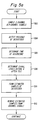
- the steps carried out by the DSP device 130 in performing these compensating methods are illustrated in the flowcharts of Figs. 5a and 5b.
- the method begins in Fig. 5a with sampling the I-channel and Q-channel signals in step 502 and detecting the presence of the interferer as described above in step 504.
- the time of the associated signal ramp's occurrence and the levels of the channel signals before and after the ramp are determined (steps 506, 508) so that estimated samples of the interfering signal can be formed (step 510).
- the estimated samples are removed from the channel signal samples (step 512), and the resulting compensated channel signal samples are further processed, e.g., for detecting or recovering the information signal transmitted.
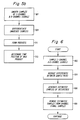
- Fig. 5b shows a flowchart of one of the above-described methods for determining the time of occurrence of the signal ramp due to the interferer (step 506 in Fig. 5a).
- the signal samples from both the I-channel and the Q-channel are smoothed, e.g., by forming sliding averages, in step 507, and the smoothed channel signals are differentiated in step 509.
- Products of the differentiated signals are formed sample-by-sample, as described above, in step 511, and the time of occurrence of the ramp is determined in step 513 from the time position of the maximal value of the products (see Fig. 3c).
- the simple method of estimating the interfering signal (second-order product) that is described above for GSM is inadequate. Adding an AM signal to the desired signal makes single-channel removal impossible.
- a direct-conversion receiver for GSM (and all quadrature modulation schemes) has two base band channels, the I- and Q-channels.
- the second-order product of an AM interferer in such a receiver should be exactly the same in both channels since the products are only related to the second-order distortions of non-linear devices (which would be equal for matched mixers) and are independent of the local oscillator's phase (and frequency).
- y I ( t ) I ( t ) + p 2 ( t )
- y Q ( t ) Q ( t ) + p 2 ( t )
- y 1 (t) is the value of a sample taken at time t of the base band signal in the I-channel
- I(t) is the ideal value of the I-channel signal sample
- p 2 (t) is the value of the second-order interfering product.
- the parameters in the expression for the Q-channel are similarly defined.
- I- and Q-channels are orthogonal, as they would be in a receiver for quadrature-modulated signals.
- Applicants' invention must be embodied in a receiver that has two channels, it is sufficient that the channels span the I-Q plane.
- the terms "in-phase signal” and “quadrature signal” should not be interpreted as requiring orthogonality, except when used in combination with others, such as “quadrature modulation”, that are conventionally understood to require such a relationship.
- the input signal-to-noise ratio (SNR) in GSM is typically at least 10 dB.
- the signal locus described by Eq. 5 is a circle having radius r in the complex plane.
- the DSP device 130 determines the samples p 2 (t) from the samples y l (t) and y Q (t) of the I- and Q-channel base-band signals and then subtract the p 2 (t) samples from the y I (t) and y Q (t) samples on a sample-by-sample basis to generate compensated samples I(t) and Q(t) of the I- and Q-channel signals. It is not even necessary to detect the presence of the interferer or second-order product signal, since the compensation according to Eq. 8 does not rely on the same characteristics of the interferer as does the compensation specific for GSM and like communication systems. Therefore, the digitally compensated direct-conversion receiver can be much more resistant to AM interference than a conventional analog receiver.
- the steps carried out by the DSP device 130 in performing this compensating method are illustrated in Fig. 6.
- the method begins with sampling the I-channel and Q-channel signals in step 602 and determining the amplitude of the desired signal by averaging differences between respective samples in step 604.
- Estimated samples of the second-order product signal are then generated in step 606 from the desired-signal amplitude and the channel signal samples.
- Compensated samples are produced in step 608 by removing these estimated samples from the channel signal samples.
- both fading and time dispersion affect the accuracy of the digital compensation. It is usually very difficult, if not impossible, to separate such signal variations from the second-order-product signal variation intended to be compensated by Applicants' invention. Even so, there are many systems in which fading and/or dispersion will not cause significant problems. For example, when the data bursts are short enough (or when the receiver's speed is low), fading should not significantly affect the compensation. Also, when the receiver is close to the transmitter (which is usually the only time when a second-order product is strong), time dispersion is low.
Landscapes
- Engineering & Computer Science (AREA)
- Computer Networks & Wireless Communication (AREA)
- Signal Processing (AREA)
- Power Engineering (AREA)
- Digital Transmission Methods That Use Modulated Carrier Waves (AREA)
- Noise Elimination (AREA)
- Superheterodyne Receivers (AREA)
- Reduction Or Emphasis Of Bandwidth Of Signals (AREA)
- Input Circuits Of Receivers And Coupling Of Receivers And Audio Equipment (AREA)
Claims (8)
- Appareil pour compenser numériquement un signal de brouillage comportant une première partie d'enveloppe constante, une partie en rampe et une seconde partie d'enveloppe constante, pour une utilisation dans un récepteur à conversion directe pour la récupération d'un signal d'information à partir d'un signal porteur modulé par le signal d'information, le récepteur comportant au moins un mélangeur, dans lequel le signal porteur modulé est séparé en un signal de bande de base en phase et un signal de bande de base en quadrature, l'appareil comportant :un moyen (120, 22) destiné à générer des échantillons numériques du signal de bande de base en phase et du signal de bande de base en quadrature ;un moyen destiné à détecter une position temporelle d'une rampe entre un premier niveau continu et un second niveau continu dans au moins l'un du signal de bande de base en phase et du signal de bande de base en quadrature ;un moyen destiné à établir une moyenne d'échantillons numériques du, au moins un, signal, le moyen d'établissement de moyenne formant une première moyenne d'échantillons numériques pendant une première période de temps avant la position temporelle et une seconde moyenne d'échantillons numériques pendant une seconde période de temps après la position temporelle,un moyen destiné à générer des échantillons estimés d'un signal de brouillage de bande de base résultant d'un produit de second ordre d'un signal de sortie du mélangeur, sur la base de la position temporelle et des première et seconde moyennes, etun moyen destiné à compenser les échantillons numériques du signal de bande de base en phase et du signal de bande de base en quadrature, en en soustrayant les échantillons estimés du signal de brouillage de bande de base.
- Appareil selon la revendication 1, dans lequel le moyen de détection comporte :un moyen destiné à lisser des échantillons numériques du, au moins un, signal,un moyen destiné à différencier des échantillons numériques lissés du, au moins un, signal, etun moyen destiné à déterminer une position temporelle d'une valeur maximale d'échantillons numériques lissés et différenciés du, au moins un, signal.
- Appareil selon la revendication 1, dans lequel le moyen de détection comporte :un moyen destiné à lisser des échantillons numériques du signal de signal de bande de base en phase et du signal de bande de base en quadrature,un moyen destiné à différencier des échantillons numériques lissés du signal en phase et du signal en quadrature,un moyen destiné à former des produits d'échantillons lissés différenciés du signal en phase et du signal en quadrature, etun moyen destiné à déterminer une position temporelle d'une valeur maximale des produits, etle moyen d'établissement de moyenne est conçu pour former une première moyenne d'échantillons numériques du signal de bande de base en phase et une première moyenne d'échantillons numériques du signal de bande de base en quadrature pendant la première période de temps avant la position temporelle, et une seconde moyenne d'échantillons numériques du signal de bande de base en phase et une seconde moyenne d'échantillons numériques du signal de bande de base en quadrature pendant la seconde période de temps après la position temporelle.
- Appareil selon la revendication 1, comportant en outre un moyen destiné à séparer le signal porteur modulé en le signal de bande de base en phase et le signal de bande de base en quadrature, sensiblement orthogonal.
- Procédé pour compenser numériquement un signal de brouillage comportant une première partie d'enveloppe constante, une partie en rampe et une seconde partie d'enveloppe constante, pour une utilisation dans un récepteur à conversion directe pour récupérer un signal d'information à partir d'un signal porteur modulé par le signal d'information, le récepteur comportant au moins un mélangeur, dans lequel le signal porteur modulé est séparé en un signal de bande de base en phase et un signal de bande de base en quadrature, le procédé comprenant :la génération d'échantillons numériques du signal de bande de base en phase et du signal de bande de base en quadrature (502) ;la détection d'une position temporelle d'une rampe entre un premier niveau continu et un second niveau continu dans au moins l'un du signal de bande de base en phase et du signal de bande de base en quadrature (506) ;la formation d'une première moyenne d'échantillons numériques du, au moins un, signal pendant une première période de temps avant la position temporelle et la formation d'une seconde moyenne d'échantillons numériques du, au moins un, signal pendant une seconde période de temps après la position temporelle (508),la génération d'échantillons estimés d'un signal de brouillage de bande de base résultant d'un produit de second ordre d'un signal de sortie du mélangeur, sur la base de la position temporelle et des première et seconde moyennes (510), etla compensation des échantillons numériques du signal de bande de base en phase et du signal de bande de base en quadrature, en en soustrayant les échantillons estimés du signal de brouillage de bande de base (512).
- Procédé selon la revendication 5, dans lequel l'étape de détection de la position temporelle comprend les étapes qui consistent :à lisser des échantillons numériques du, au moins un, signal,à différencier les échantillons numériques lissés du, au moins un, signal, età déterminer une position temporelle d'une valeur maximale des échantillons numériques lissés différenciés du, au moins un, signal.
- Procédé selon la revendication 5, dans lequel l'étape de détection de la position temporelle comprend les étapes qui consistent :dans lequel l'étape de formation de la première moyenne comprend la formation d'une première moyenne d'échantillons numériques du signal de bande de base en phase et d'une première moyenne d'échantillons numériques du signal de bande de base en quadrature pendant une première période de temps avant la position temporelle, età lisser des échantillons numériques du signal de bande de base en phase et du signal de bande de base en quadrature,à différencier des échantillons numériques lissés du signal en phase et du signal en quadrature,à former des produits d'échantillons lissés différenciés du signal en phase et du signal en quadrature, età déterminer une position temporelle d'une valeur maximale des produits ;
dans lequel l'étape de formation de la seconde moyenne comprend la formation d'une seconde moyenne d'échantillons numériques du signal de bande de base en phase et d'une seconde moyenne d'échantillons numériques du signal de bande de base en quadrature pendant une seconde période de temps après la position temporelle. - Procédé selon la revendication 5, comprenant en outre l'étape de séparation du signal porteur modulé en le signal de bande de base en phase et le signal de bande de base en quadrature, sensiblement orthogonal.
Priority Applications (1)
| Application Number | Priority Date | Filing Date | Title |
|---|---|---|---|
| EP03020410A EP1391997B1 (fr) | 1994-12-28 | 1995-12-19 | Récepteur à conversion directe et à compensation numérique |
Applications Claiming Priority (3)
| Application Number | Priority Date | Filing Date | Title |
|---|---|---|---|
| US365037 | 1994-12-28 | ||
| US08/365,037 US5579347A (en) | 1994-12-28 | 1994-12-28 | Digitally compensated direct conversion receiver |
| PCT/SE1995/001546 WO1996020539A1 (fr) | 1994-12-28 | 1995-12-19 | Recepteur a conversion directe et a compensation numerique |
Related Child Applications (1)
| Application Number | Title | Priority Date | Filing Date |
|---|---|---|---|
| EP03020410A Division EP1391997B1 (fr) | 1994-12-28 | 1995-12-19 | Récepteur à conversion directe et à compensation numérique |
Publications (2)
| Publication Number | Publication Date |
|---|---|
| EP0835557A1 EP0835557A1 (fr) | 1998-04-15 |
| EP0835557B1 true EP0835557B1 (fr) | 2004-06-16 |
Family
ID=23437213
Family Applications (2)
| Application Number | Title | Priority Date | Filing Date |
|---|---|---|---|
| EP95942346A Expired - Lifetime EP0835557B1 (fr) | 1994-12-28 | 1995-12-19 | Recepteur a conversion directe et a compensation numerique |
| EP03020410A Expired - Lifetime EP1391997B1 (fr) | 1994-12-28 | 1995-12-19 | Récepteur à conversion directe et à compensation numérique |
Family Applications After (1)
| Application Number | Title | Priority Date | Filing Date |
|---|---|---|---|
| EP03020410A Expired - Lifetime EP1391997B1 (fr) | 1994-12-28 | 1995-12-19 | Récepteur à conversion directe et à compensation numérique |
Country Status (14)
| Country | Link |
|---|---|
| US (1) | US5579347A (fr) |
| EP (2) | EP0835557B1 (fr) |
| JP (1) | JPH10513616A (fr) |
| KR (1) | KR100379723B1 (fr) |
| CN (2) | CN1146119C (fr) |
| AU (1) | AU698865B2 (fr) |
| BR (1) | BR9510108A (fr) |
| CA (1) | CA2208850A1 (fr) |
| DE (2) | DE69535256D1 (fr) |
| FI (1) | FI114670B (fr) |
| NO (1) | NO972985L (fr) |
| PL (1) | PL184618B1 (fr) |
| RU (1) | RU2146416C1 (fr) |
| WO (1) | WO1996020539A1 (fr) |
Cited By (1)
| Publication number | Priority date | Publication date | Assignee | Title |
|---|---|---|---|---|
| WO2006114018A1 (fr) * | 2005-04-26 | 2006-11-02 | Zte Corporation | Echangeur de donnees en bandes de base multiples et son procede |
Families Citing this family (83)
| Publication number | Priority date | Publication date | Assignee | Title |
|---|---|---|---|---|
| US5864754A (en) * | 1996-02-05 | 1999-01-26 | Hotto; Robert | System and method for radio signal reconstruction using signal processor |
| US8280334B2 (en) | 1996-02-05 | 2012-10-02 | American Radio Llc | System and method for radio signal reconstruction using signal processor |
| EP0824782B1 (fr) * | 1996-02-29 | 2001-10-24 | Koninklijke Philips Electronics N.V. | Recepteur pourvu d'un traitement numerique de signal d'entree divise en phases |
| US5838735A (en) * | 1996-07-08 | 1998-11-17 | Telefonaktiebolaget Lm Ericsson | Method and apparatus for compensating for a varying d.c. offset in a sampled signal |
| US5749051A (en) * | 1996-07-18 | 1998-05-05 | Ericsson Inc. | Compensation for second order intermodulation in a homodyne receiver |
| US5918169A (en) * | 1996-09-25 | 1999-06-29 | Ericsson, Inc. | Homodyne cellular base station |
| US5963856A (en) * | 1997-01-03 | 1999-10-05 | Lucent Technologies Inc | Wireless receiver including tunable RF bandpass filter |
| JP3860292B2 (ja) * | 1997-06-24 | 2006-12-20 | 大井電気株式会社 | 周波数シフトキーイング信号の復調方法 |
| US6029052A (en) * | 1997-07-01 | 2000-02-22 | Telefonaktiebolaget Lm Ericsson | Multiple-mode direct conversion receiver |
| US6021323A (en) * | 1997-09-25 | 2000-02-01 | Rockwell Science Center, Inc. | Direct conversion receiver with reduced even order distortion |
| JPH11234150A (ja) * | 1998-02-09 | 1999-08-27 | Toshiba Corp | デジタル復調装置 |
| US6088581A (en) * | 1998-03-27 | 2000-07-11 | Motorola, Inc. | Method and apparatus for reducing amplitude modulated interference in a receiver |
| US7515896B1 (en) | 1998-10-21 | 2009-04-07 | Parkervision, Inc. | Method and system for down-converting an electromagnetic signal, and transforms for same, and aperture relationships |
| US6061551A (en) | 1998-10-21 | 2000-05-09 | Parkervision, Inc. | Method and system for down-converting electromagnetic signals |
| US6694128B1 (en) | 1998-08-18 | 2004-02-17 | Parkervision, Inc. | Frequency synthesizer using universal frequency translation technology |
| US6091940A (en) | 1998-10-21 | 2000-07-18 | Parkervision, Inc. | Method and system for frequency up-conversion |
| US7065327B1 (en) | 1998-09-10 | 2006-06-20 | Intel Corporation | Single-chip CMOS direct-conversion transceiver |
| US7039372B1 (en) | 1998-10-21 | 2006-05-02 | Parkervision, Inc. | Method and system for frequency up-conversion with modulation embodiments |
| US6560301B1 (en) | 1998-10-21 | 2003-05-06 | Parkervision, Inc. | Integrated frequency translation and selectivity with a variety of filter embodiments |
| US6061555A (en) | 1998-10-21 | 2000-05-09 | Parkervision, Inc. | Method and system for ensuring reception of a communications signal |
| US7027786B1 (en) | 1998-10-21 | 2006-04-11 | Parkervision, Inc. | Carrier and clock recovery using universal frequency translation |
| US6542722B1 (en) | 1998-10-21 | 2003-04-01 | Parkervision, Inc. | Method and system for frequency up-conversion with variety of transmitter configurations |
| US6370371B1 (en) | 1998-10-21 | 2002-04-09 | Parkervision, Inc. | Applications of universal frequency translation |
| US7295826B1 (en) | 1998-10-21 | 2007-11-13 | Parkervision, Inc. | Integrated frequency translation and selectivity with gain control functionality, and applications thereof |
| US6049706A (en) | 1998-10-21 | 2000-04-11 | Parkervision, Inc. | Integrated frequency translation and selectivity |
| US6813485B2 (en) | 1998-10-21 | 2004-11-02 | Parkervision, Inc. | Method and system for down-converting and up-converting an electromagnetic signal, and transforms for same |
| US7236754B2 (en) | 1999-08-23 | 2007-06-26 | Parkervision, Inc. | Method and system for frequency up-conversion |
| WO2000039923A1 (fr) | 1998-12-24 | 2000-07-06 | Telefonaktiebolaget Lm Ericsson (Publ) | Recepteur de communication ayant une plage dynamique reduite |
| US7006805B1 (en) | 1999-01-22 | 2006-02-28 | Parker Vision, Inc. | Aliasing communication system with multi-mode and multi-band functionality and embodiments thereof, such as the family radio service |
| US6704549B1 (en) | 1999-03-03 | 2004-03-09 | Parkvision, Inc. | Multi-mode, multi-band communication system |
| US6704558B1 (en) | 1999-01-22 | 2004-03-09 | Parkervision, Inc. | Image-reject down-converter and embodiments thereof, such as the family radio service |
| SE9900289D0 (sv) * | 1999-01-27 | 1999-01-27 | Ericsson Telefon Ab L M | DC estimate method for a homodyne receiver |
| US6879817B1 (en) | 1999-04-16 | 2005-04-12 | Parkervision, Inc. | DC offset, re-radiation, and I/Q solutions using universal frequency translation technology |
| US6853690B1 (en) | 1999-04-16 | 2005-02-08 | Parkervision, Inc. | Method, system and apparatus for balanced frequency up-conversion of a baseband signal and 4-phase receiver and transceiver embodiments |
| US6873836B1 (en) | 1999-03-03 | 2005-03-29 | Parkervision, Inc. | Universal platform module and methods and apparatuses relating thereto enabled by universal frequency translation technology |
| US7110435B1 (en) | 1999-03-15 | 2006-09-19 | Parkervision, Inc. | Spread spectrum applications of universal frequency translation |
| US7065162B1 (en) | 1999-04-16 | 2006-06-20 | Parkervision, Inc. | Method and system for down-converting an electromagnetic signal, and transforms for same |
| US7693230B2 (en) | 1999-04-16 | 2010-04-06 | Parkervision, Inc. | Apparatus and method of differential IQ frequency up-conversion |
| US7110444B1 (en) | 1999-08-04 | 2006-09-19 | Parkervision, Inc. | Wireless local area network (WLAN) using universal frequency translation technology including multi-phase embodiments and circuit implementations |
| US7072390B1 (en) | 1999-08-04 | 2006-07-04 | Parkervision, Inc. | Wireless local area network (WLAN) using universal frequency translation technology including multi-phase embodiments |
| US7054296B1 (en) | 1999-08-04 | 2006-05-30 | Parkervision, Inc. | Wireless local area network (WLAN) technology and applications including techniques of universal frequency translation |
| US8295406B1 (en) | 1999-08-04 | 2012-10-23 | Parkervision, Inc. | Universal platform module for a plurality of communication protocols |
| MY133723A (en) * | 1999-09-17 | 2007-11-30 | Ericsson Telefon Ab L M | "apparatus and method for substantially eliminating a near-channel interfering amplitude modulated signal" |
| US6373909B2 (en) * | 1999-10-22 | 2002-04-16 | Telefonaktiebolaget Lm Ericsson (Publ) | Communications terminal having a receiver and method for removing known interferers from a digitized intermediate frequency signal |
| US7082171B1 (en) | 1999-11-24 | 2006-07-25 | Parkervision, Inc. | Phase shifting applications of universal frequency translation |
| US6631170B1 (en) * | 1999-12-03 | 2003-10-07 | Nokia Corporation | Radio frequency receiver |
| US6963734B2 (en) | 1999-12-22 | 2005-11-08 | Parkervision, Inc. | Differential frequency down-conversion using techniques of universal frequency translation technology |
| US7292835B2 (en) | 2000-01-28 | 2007-11-06 | Parkervision, Inc. | Wireless and wired cable modem applications of universal frequency translation technology |
| US6259752B1 (en) * | 2000-02-01 | 2001-07-10 | Conexant Systems, Inc. | System for cancelling internal interference in a receiver |
| US7010286B2 (en) | 2000-04-14 | 2006-03-07 | Parkervision, Inc. | Apparatus, system, and method for down-converting and up-converting electromagnetic signals |
| US7554508B2 (en) | 2000-06-09 | 2009-06-30 | Parker Vision, Inc. | Phased array antenna applications on universal frequency translation |
| GB2366460A (en) * | 2000-08-24 | 2002-03-06 | Nokia Mobile Phones Ltd | DC compensation for a direct conversion radio receiver |
| US6600913B1 (en) * | 2000-10-27 | 2003-07-29 | Sony International (Europe) Gmbh | Two-port demodulation device |
| ATE313166T1 (de) * | 2000-10-30 | 2005-12-15 | Texas Instruments Inc | Vorrichtung zum ausgleichen des dc-offsets eines quadratur-demodulators , und verfahren dazu |
| EP1202511B1 (fr) * | 2000-10-30 | 2006-01-11 | Texas Instruments France | Procédé pour estimer et supprimer un décalage de composante continue variant dans le temps |
| US7010559B2 (en) | 2000-11-14 | 2006-03-07 | Parkervision, Inc. | Method and apparatus for a parallel correlator and applications thereof |
| US7454453B2 (en) | 2000-11-14 | 2008-11-18 | Parkervision, Inc. | Methods, systems, and computer program products for parallel correlation and applications thereof |
| EP1371200B1 (fr) * | 2001-03-01 | 2011-10-12 | Broadcom Corporation | Convertisseur serie-parallele de traitement de signaux numeriques |
| US6731906B2 (en) * | 2001-04-23 | 2004-05-04 | University Corporation For Atmospheric Research | Method and system for determining the phase and amplitude of a radio occultation signal |
| DE10128236A1 (de) * | 2001-06-11 | 2002-08-01 | Infineon Technologies Ag | Verfahren zur Kompensation einer stufenförmigen DC-Störung in einem digitalen Basisbandsignal eines Homodyn-Funkempfängers |
| US7072427B2 (en) | 2001-11-09 | 2006-07-04 | Parkervision, Inc. | Method and apparatus for reducing DC offsets in a communication system |
| US7085335B2 (en) | 2001-11-09 | 2006-08-01 | Parkervision, Inc. | Method and apparatus for reducing DC offsets in a communication system |
| US7356326B2 (en) * | 2001-12-12 | 2008-04-08 | Samsung Electronics Co., Ltd. | Direct-conversion receiver for removing DC offset |
| US6959170B2 (en) * | 2001-12-20 | 2005-10-25 | Motorola, Inc. | Communications receivers and methods therefor |
| US6975848B2 (en) | 2002-06-04 | 2005-12-13 | Parkervision, Inc. | Method and apparatus for DC offset removal in a radio frequency communication channel |
| US7321640B2 (en) | 2002-06-07 | 2008-01-22 | Parkervision, Inc. | Active polyphase inverter filter for quadrature signal generation |
| US6700453B2 (en) * | 2002-06-18 | 2004-03-02 | Nokia Corporation | Amplitude imbalance compensation of quadrature modulator |
| US7379883B2 (en) | 2002-07-18 | 2008-05-27 | Parkervision, Inc. | Networking methods and systems |
| US7460584B2 (en) | 2002-07-18 | 2008-12-02 | Parkervision, Inc. | Networking methods and systems |
| US7043208B2 (en) * | 2002-10-15 | 2006-05-09 | Motorola, Inc. | Method and apparatus to reduce interference in a communication device |
| EP1503508B1 (fr) * | 2003-07-30 | 2007-06-06 | Texas Instruments Incorporated | Réduction de décalage en continu dynamique dans un récepteur radio |
| ATE487272T1 (de) * | 2004-05-19 | 2010-11-15 | Ericsson Telefon Ab L M | Adaptives vorverzerrungsverfahren und anordnung |
| US7680456B2 (en) * | 2005-02-16 | 2010-03-16 | Texas Instruments Incorporated | Methods and apparatus to perform signal removal in a low intermediate frequency receiver |
| KR101261527B1 (ko) * | 2006-10-27 | 2013-05-06 | 삼성전자주식회사 | 직접 변환 구조의 rf 쿼드러쳐 송수신기에서 부정합을보상하는 방법 및 장치 |
| KR100808244B1 (ko) * | 2006-12-15 | 2008-03-03 | 한국과학기술원 | 다중 모드에 따른 입력 임피던스 매칭을 이용하는 무선식별 시스템 |
| GB0803710D0 (en) * | 2008-02-28 | 2008-04-09 | Nokia Corp | DC compensation |
| CN101741788B (zh) * | 2009-11-27 | 2012-10-03 | 许昌学院 | 最小频移键控信号的调制解调方法及专用的复解析带通滤波器设计方法 |
| EP3441976A1 (fr) * | 2013-03-14 | 2019-02-13 | M. Zubair Mirza | Système de surveillance de maladie basé sur internet (idms) |
| RU2542939C1 (ru) * | 2013-10-09 | 2015-02-27 | Общество с ограниченной ответственностью "Алсет Веллен" | Приемник прямого преобразования с квадратурно-трехфазной архитектурой, способ прямого преобразования сигнала посредством указанного приемника и способ управления настройкой указанного приемника |
| US10317535B2 (en) * | 2016-03-31 | 2019-06-11 | Samsung Electronics Co., Ltd | Method and apparatus for second order intercept point (IP2) calibration |
| KR20240078786A (ko) | 2022-11-28 | 2024-06-04 | 주식회사 피오 | 다공성 멤브레인 초음파진동 절단장치 |
| KR102775710B1 (ko) | 2024-10-18 | 2025-03-05 | 에스피씨케이(주) | 파이프연결용 커플링 나사산 자동가공방법 |
| KR102901723B1 (ko) | 2024-10-22 | 2025-12-31 | 동서대학교 산학협력단 | 적설 제거형 낙하물 방지망 지지기구 |
Family Cites Families (17)
| Publication number | Priority date | Publication date | Assignee | Title |
|---|---|---|---|---|
| GB1536850A (en) * | 1975-09-15 | 1978-12-20 | Racal Instruments Ltd | Electrical measuring and noise suppression circuitry |
| US4416017A (en) * | 1981-01-05 | 1983-11-15 | Motorola, Inc. | Apparatus and method for attenuating interfering signals |
| DE3240565C2 (de) * | 1982-11-03 | 1985-12-12 | Telefunken electronic GmbH, 6000 Frankfurt | Direktmischender Synchronempfänger |
| GB2149244B (en) * | 1983-10-29 | 1987-01-21 | Standard Telephones Cables Ltd | Digital demodulator arrangement for quadrature signals |
| JPS61171207A (ja) * | 1985-01-25 | 1986-08-01 | Nec Corp | 受信機 |
| US4736455A (en) * | 1985-12-23 | 1988-04-05 | Nippon Telegraph And Telephone Corporation | Interference cancellation system |
| JPH0630449B2 (ja) * | 1987-03-03 | 1994-04-20 | 富士通株式会社 | 干渉検出装置 |
| GB8728577D0 (en) * | 1987-12-07 | 1988-01-13 | Secr Defence | Improvements in/relating to modulation enhancement |
| NL8802531A (nl) * | 1988-10-14 | 1990-05-01 | Philips Nv | Fasedetector en frequentiedemodulator voorzien van zulk een fasedetector. |
| US4970459A (en) * | 1988-12-02 | 1990-11-13 | General Electric Company | Electronic meter chopper stabilization |
| GB9015059D0 (en) * | 1990-07-09 | 1990-08-29 | C Com Group Plc | Radio receivers |
| US5241702A (en) * | 1990-09-06 | 1993-08-31 | Telefonaktiebolaget L M Ericsson | D.c. offset compensation in a radio receiver |
| FI98580C (fi) * | 1991-11-14 | 1997-07-10 | Nokia Mobile Phones Ltd | Selektiivisyyssuodatus solukkopuhelimessa |
| DE69228816T2 (de) * | 1992-10-28 | 1999-08-19 | Alcatel | Offsetgleichspannungskorrektur für Direktmisch-TDMA-Empfänger |
| DE4238542C1 (de) * | 1992-11-14 | 1994-06-09 | Hagenuk Telecom Gmbh | Verfahren und Vorrichtung zur Korrektur von Gleichspannungs-Fehlersignalen bei direktmischenden Empfangseinrichtungen |
| JPH06177787A (ja) * | 1992-12-01 | 1994-06-24 | Nippon Telegr & Teleph Corp <Ntt> | 干渉補償回路 |
| US5369411A (en) * | 1993-06-01 | 1994-11-29 | Westinghouse Electric Corporation | Imbalance correction of in-phase and quadrature phase return signals |
-
1994
- 1994-12-28 US US08/365,037 patent/US5579347A/en not_active Expired - Lifetime
-
1995
- 1995-12-19 CN CNB011377674A patent/CN1146119C/zh not_active Expired - Fee Related
- 1995-12-19 EP EP95942346A patent/EP0835557B1/fr not_active Expired - Lifetime
- 1995-12-19 WO PCT/SE1995/001546 patent/WO1996020539A1/fr not_active Ceased
- 1995-12-19 CA CA002208850A patent/CA2208850A1/fr not_active Abandoned
- 1995-12-19 PL PL95321059A patent/PL184618B1/pl not_active IP Right Cessation
- 1995-12-19 DE DE69535256T patent/DE69535256D1/de not_active Expired - Lifetime
- 1995-12-19 DE DE69533175T patent/DE69533175T2/de not_active Expired - Fee Related
- 1995-12-19 RU RU97112905A patent/RU2146416C1/ru not_active IP Right Cessation
- 1995-12-19 AU AU43596/96A patent/AU698865B2/en not_active Ceased
- 1995-12-19 BR BR9510108A patent/BR9510108A/pt not_active IP Right Cessation
- 1995-12-19 KR KR1019970704455A patent/KR100379723B1/ko not_active Expired - Fee Related
- 1995-12-19 EP EP03020410A patent/EP1391997B1/fr not_active Expired - Lifetime
- 1995-12-19 JP JP8520403A patent/JPH10513616A/ja not_active Ceased
- 1995-12-19 CN CN95197646A patent/CN1086066C/zh not_active Expired - Fee Related
-
1997
- 1997-06-26 NO NO972985A patent/NO972985L/no not_active Application Discontinuation
- 1997-06-27 FI FI972786A patent/FI114670B/fi not_active IP Right Cessation
Cited By (1)
| Publication number | Priority date | Publication date | Assignee | Title |
|---|---|---|---|---|
| WO2006114018A1 (fr) * | 2005-04-26 | 2006-11-02 | Zte Corporation | Echangeur de donnees en bandes de base multiples et son procede |
Also Published As
| Publication number | Publication date |
|---|---|
| CN1392672A (zh) | 2003-01-22 |
| DE69533175T2 (de) | 2005-07-14 |
| US5579347A (en) | 1996-11-26 |
| AU4359696A (en) | 1996-07-19 |
| FI972786A7 (fi) | 1997-08-22 |
| KR100379723B1 (ko) | 2003-06-09 |
| EP0835557A1 (fr) | 1998-04-15 |
| PL321059A1 (en) | 1997-11-24 |
| EP1391997A3 (fr) | 2004-06-02 |
| PL184618B1 (pl) | 2002-11-29 |
| BR9510108A (pt) | 1997-11-25 |
| FI114670B (fi) | 2004-11-30 |
| CN1146119C (zh) | 2004-04-14 |
| CA2208850A1 (fr) | 1996-07-04 |
| JPH10513616A (ja) | 1998-12-22 |
| NO972985L (no) | 1997-08-25 |
| NO972985D0 (no) | 1997-06-26 |
| FI972786A0 (fi) | 1997-06-27 |
| RU2146416C1 (ru) | 2000-03-10 |
| DE69535256D1 (de) | 2006-11-16 |
| EP1391997B1 (fr) | 2006-10-04 |
| EP1391997A2 (fr) | 2004-02-25 |
| CN1086066C (zh) | 2002-06-05 |
| CN1175328A (zh) | 1998-03-04 |
| WO1996020539A1 (fr) | 1996-07-04 |
| AU698865B2 (en) | 1998-11-12 |
| MX9704753A (es) | 1997-10-31 |
| DE69533175D1 (de) | 2004-07-22 |
Similar Documents
| Publication | Publication Date | Title |
|---|---|---|
| EP0835557B1 (fr) | Recepteur a conversion directe et a compensation numerique | |
| US5838735A (en) | Method and apparatus for compensating for a varying d.c. offset in a sampled signal | |
| US6922555B1 (en) | Phase interpolation receiver for angle modulated RF signals | |
| EP1214795B1 (fr) | Procede et appareil de compensation de perturbations d'un recepteur a conversion directe place dans un emetteur-recepteur duplex integral | |
| EP0706730B1 (fr) | Procede et appareil de commande de gain automatique et d'annulation de decalage cc dans un recepteur a quadrature | |
| US7200188B2 (en) | Method and apparatus for frequency offset compensation | |
| WO2003012979A1 (fr) | Emetteur-recepteur en quadrature ne presentant sensiblement aucun effet indesirable de defaut d'adaptation de circuits | |
| RU2241310C2 (ru) | Гомодинный радиоприемник | |
| US20080181284A1 (en) | Hybrid Zero-IF Receiver | |
| JP4717309B2 (ja) | 多相受信機における改良、又は多相受信機に関する改良 | |
| JP2002043962A (ja) | 通信システムにおける受信方法及び受信機 | |
| MXPA97004753A (en) | Receiver of direct conversion, compensated digitalme | |
| JPH0823361A (ja) | Tdmaデータ受信装置 | |
| HK1005920B (en) | Method and apparatus for automatic gain control and dc offset cancellation in quadrature receiver |
Legal Events
| Date | Code | Title | Description |
|---|---|---|---|
| PUAI | Public reference made under article 153(3) epc to a published international application that has entered the european phase |
Free format text: ORIGINAL CODE: 0009012 |
|
| 17P | Request for examination filed |
Effective date: 19970530 |
|
| AK | Designated contracting states |
Kind code of ref document: A1 Designated state(s): BE DE DK ES FR GB GR IT NL PT SE |
|
| 17Q | First examination report despatched |
Effective date: 20030313 |
|
| RIN1 | Information on inventor provided before grant (corrected) |
Inventor name: GUSTAFSSON, KJELL Inventor name: SALLENHAG, MARTIN Inventor name: WENDELRUP, HEINO Inventor name: ISBERG, MARTIN Inventor name: LINDQUIST, BJOERN |
|
| GRAP | Despatch of communication of intention to grant a patent |
Free format text: ORIGINAL CODE: EPIDOSNIGR1 |
|
| GRAS | Grant fee paid |
Free format text: ORIGINAL CODE: EPIDOSNIGR3 |
|
| GRAA | (expected) grant |
Free format text: ORIGINAL CODE: 0009210 |
|
| RAP1 | Party data changed (applicant data changed or rights of an application transferred) |
Owner name: TELEFONAKTIEBOLAGET LM ERICSSON (PUBL) |
|
| AK | Designated contracting states |
Kind code of ref document: B1 Designated state(s): BE DE DK ES FR GB GR IT NL PT SE |
|
| PG25 | Lapsed in a contracting state [announced via postgrant information from national office to epo] |
Ref country code: NL Free format text: LAPSE BECAUSE OF FAILURE TO SUBMIT A TRANSLATION OF THE DESCRIPTION OR TO PAY THE FEE WITHIN THE PRESCRIBED TIME-LIMIT Effective date: 20040616 Ref country code: IT Free format text: LAPSE BECAUSE OF FAILURE TO SUBMIT A TRANSLATION OF THE DESCRIPTION OR TO PAY THE FEE WITHIN THE PRE;WARNING: LAPSES OF ITALIAN PATENTS WITH EFFECTIVE DATE BEFORE 2007 MAY HAVE OCCURRED AT ANY TIME BEFORE 2007. THE CORRECT EFFECTIVE DATE MAY BE DIFFERENT FROM THE ONE RECORDED.SCRIBED TIME-LIMIT Effective date: 20040616 Ref country code: FR Free format text: LAPSE BECAUSE OF NON-PAYMENT OF DUE FEES Effective date: 20040616 Ref country code: BE Free format text: LAPSE BECAUSE OF FAILURE TO SUBMIT A TRANSLATION OF THE DESCRIPTION OR TO PAY THE FEE WITHIN THE PRESCRIBED TIME-LIMIT Effective date: 20040616 |
|
| REG | Reference to a national code |
Ref country code: GB Ref legal event code: FG4D |
|
| REF | Corresponds to: |
Ref document number: 69533175 Country of ref document: DE Date of ref document: 20040722 Kind code of ref document: P |
|
| PG25 | Lapsed in a contracting state [announced via postgrant information from national office to epo] |
Ref country code: SE Free format text: LAPSE BECAUSE OF FAILURE TO SUBMIT A TRANSLATION OF THE DESCRIPTION OR TO PAY THE FEE WITHIN THE PRESCRIBED TIME-LIMIT Effective date: 20040916 Ref country code: GR Free format text: LAPSE BECAUSE OF FAILURE TO SUBMIT A TRANSLATION OF THE DESCRIPTION OR TO PAY THE FEE WITHIN THE PRESCRIBED TIME-LIMIT Effective date: 20040916 Ref country code: DK Free format text: LAPSE BECAUSE OF FAILURE TO SUBMIT A TRANSLATION OF THE DESCRIPTION OR TO PAY THE FEE WITHIN THE PRESCRIBED TIME-LIMIT Effective date: 20040916 |
|
| PG25 | Lapsed in a contracting state [announced via postgrant information from national office to epo] |
Ref country code: ES Free format text: LAPSE BECAUSE OF FAILURE TO SUBMIT A TRANSLATION OF THE DESCRIPTION OR TO PAY THE FEE WITHIN THE PRESCRIBED TIME-LIMIT Effective date: 20040927 |
|
| NLV1 | Nl: lapsed or annulled due to failure to fulfill the requirements of art. 29p and 29m of the patents act | ||
| PG25 | Lapsed in a contracting state [announced via postgrant information from national office to epo] |
Ref country code: GB Free format text: LAPSE BECAUSE OF NON-PAYMENT OF DUE FEES Effective date: 20041219 |
|
| PLBE | No opposition filed within time limit |
Free format text: ORIGINAL CODE: 0009261 |
|
| STAA | Information on the status of an ep patent application or granted ep patent |
Free format text: STATUS: NO OPPOSITION FILED WITHIN TIME LIMIT |
|
| 26N | No opposition filed |
Effective date: 20050317 |
|
| EN | Fr: translation not filed | ||
| GBPC | Gb: european patent ceased through non-payment of renewal fee |
Effective date: 20041219 |
|
| PG25 | Lapsed in a contracting state [announced via postgrant information from national office to epo] |
Ref country code: PT Free format text: LAPSE BECAUSE OF NON-PAYMENT OF DUE FEES Effective date: 20041116 |
|
| PGFP | Annual fee paid to national office [announced via postgrant information from national office to epo] |
Ref country code: DE Payment date: 20090202 Year of fee payment: 14 |
|
| PG25 | Lapsed in a contracting state [announced via postgrant information from national office to epo] |
Ref country code: DE Free format text: LAPSE BECAUSE OF NON-PAYMENT OF DUE FEES Effective date: 20100701 |