EP0837517B1 - Filtre diélectrique statifié et dispositif de communication - Google Patents
Filtre diélectrique statifié et dispositif de communication Download PDFInfo
- Publication number
- EP0837517B1 EP0837517B1 EP97117967A EP97117967A EP0837517B1 EP 0837517 B1 EP0837517 B1 EP 0837517B1 EP 97117967 A EP97117967 A EP 97117967A EP 97117967 A EP97117967 A EP 97117967A EP 0837517 B1 EP0837517 B1 EP 0837517B1
- Authority
- EP
- European Patent Office
- Prior art keywords
- electrodes
- dielectric
- dielectric laminated
- strip line
- electrode
- Prior art date
- Legal status (The legal status is an assumption and is not a legal conclusion. Google has not performed a legal analysis and makes no representation as to the accuracy of the status listed.)
- Expired - Lifetime
Links
Images




Classifications
-
- H—ELECTRICITY
- H01—ELECTRIC ELEMENTS
- H01P—WAVEGUIDES; RESONATORS, LINES, OR OTHER DEVICES OF THE WAVEGUIDE TYPE
- H01P1/00—Auxiliary devices
- H01P1/20—Frequency-selective devices, e.g. filters
- H01P1/201—Filters for transverse electromagnetic waves
- H01P1/203—Strip line filters
- H01P1/2039—Galvanic coupling between Input/Output
Definitions
- the present invention relates to a small dielectric laminated filter mainly used for a high frequency radio apparatus such as a portable telephone and a communication apparatus.
- Figure 13 shows an exploded perspective view of a conventional dielectric laminated filter.
- Figure 14 shows a laminated body constituted by laminating the layers shown in Figure 13 which are dissembled, as seen from the direction shown by arrow A.
- Figure 15 is a cutaway cross sectional view in which the filter is cut along line D-D shown in Figure 13.
- reference numerals 101, 102, 103, 104, 105, 106, and 107 designate dielectric sheets.
- Reference numerals 108a and 108b designate strip line electrodes formed on a dielectric sheet 105.
- Reference numerals 109a and 109b denote I/O line electrodes, 110a and 110b are notch capacitance electrodes, 111 is a coupling line electrode, and these inner electrodes are formed on the dielectric sheets 106, 104, and 102, respectively.
- dielectric sheets are laminated to form a dielectric laminated block on which shield electrodes 115 and 116 are formed on its top and bottom surfaces, respectively.
- I/O electrodes 117a and 117b and a ground electrode 118 are formed on the outer circumferential side of the dielectric laminated block.
- the shield electrodes 115 and 116 are grounded via the ground electrode 118.
- one end of each of the strip line electrodes 108a and 108b is grounded via the ground electrode 118 to constitute quarter-wavelength strip line resonators.
- the coupling line electrode 111 and the I/O line electrodes 109a and 109b act as a distributed constant line.
- a notch capacitance is provided between the notch capacity electrode 110a or 110b and the strip line electrode 108a or 108b.
- the notch capacitance electrodes 110a and 110b are connected together via the coupling line electrode 111 to connect the two strip line resonators in parallel via the notch capacity, and one ends of the I/O line electrodes 109a and 109b are connected to the notch capacitance electrodes 110a and 110b with the other ends connected to the I/O electrodes 117a and 117b in order to constitute a band elimination filter.
- earth electrodes 112, 113, and 114 are formed between the strip line electrodes 108a and 108b, between the I/O line electrodes 109a and 109b, and between the notch capacitance electrodes 110a and 110b, respectively.
- a shield electrode 120 is formed on the dielectric sheet 103.
- a dielectric laminated filter of this configuration is shown in, for example, Japanese Patent Application Laid-Open No. 6-268410.
- the conventional prevention of the electromagnetic coupling between the strip lines 108a and 108b using the earth electrode 112, the electromagnetic coupling between the notch capacitance electrodes 110a and 110b using the earth electrode 113, and the electromagnetic coupling between the I/O lines 109a and 109b using the earth electrode 114 is all imperfect and inductance is in fact provided in the earth electrodes 112, 113, and 114.
- unwanted electromagnetic coupling occurs between the strip line electrodes 108a and 108b and the earth electrode 112, between the I/O line electrodes 109a and 109b and the earth electrode 113, and between the notch capacitance electrodes 110a and 110b and the earth electrode 114.
- the earth electrodes 112, 113, and 114 disturb the distribution of electromagnetic fields from the strip line electrodes 108a and 108b, the I/O line electrodes 109a and 109b, and the notch capacitance electrodes 110a and 110b to degrade the unloaded Q. As a result, a good band elimination filter characteristic cannot be achieved easily.
- Reference JP-A-08 097603 describes a dielectric filter which is formed by a plurality of laminated dielectric layers. Input/output conductors are formed on the surface of an inner layer, and first and second inner conductors are formed on the surface of other inner layers. A shield layer is provided on the surface of a dielectric layer arranged between the layers of the first and second inner conductors.
- EP-A-0 638 953 relates to a dielectric filter comprising a plurality of resonators formed on a multi-layer dielectric substrate. Some of the inner layers have formed thereon a first, second and third resonator. These resonator layers are separated respectively by shielding layers.
- JP-A-06 268411 describes a multi-layer filter which is formed by combining ten dielectric substrates.
- Resonance electrodes are provided on two of the inner layers.
- the resonance electrodes are connected by a connecting transmission line provided on a layer in between.
- Ground electrodes are formed on layers in between to provide a shielding layer between the resonators and the connection layer.
- EP-A-0 641 035 describes a laminated dielectric filter having resonator electrodes provided on two of the inner layers. Shield electrode layers are arranged on intermediate layers and coupling capacitor electrodes are arranged on layers adjacent to the resonator layers.
- a first and a second dielectric laminated blocks can be laminated via the shield electrodes to eliminate the unwanted electromagnetic coupling between strip line resonators and a coupling element, thereby enabling easy design.
- This filter also provides a good band elimination filter characteristic to increase the degree of freedom for design and can be made smaller by increasing the dielectric constant of dielectric sheets.
- the wavelength can be increased without increasing the 'size of the laminated body, so the size of the resonators and thus the filter can be reduced.
- the filter characteristics can be adjusted.
- a dielectric laminated filter may further comprise said connection electrode which has a plurality of electrodes that are each formed on either of a pair of opposite surfaces among the outer surfaces and wherein said electrode is formed in an area other than the center of the surface.
- the dielectric laminated filter can, for example, provide the same potential between shield electrodes and maintain a constant potential distribution within each shield electrode, thereby providing stable filter characteristics with excellent shielding.
- a dielectric laminated filter may further comprise a shield electrode which is formed all over all the outer sides of said first dielectric laminated block other than the one on which said third resonance electrode is formed.
- the dielectric laminated filter can, for example, improve the shielding of the first resonance electrodes with a large magnetic density to reduce radiation losses.
- a dielectric laminated filter may further include an outer dielectric sheet laminated on an outer surface of said second shield electrode, wherein one end of said third resonance electrode which extends up to the top surface of said outer dielectric sheet.
- the dielectric laminated filter can, for example, form ground capacities between the third resonance electrodes and the second shield electrodes to reduce the wavelength of the resonators.
- the ground capacity can be varied to adjust the resonance frequency of the resonators. That is, this filter can absorb the dispersion of dielectric sheets and electrode patterns.
- a dielectric laminated filter may comprise said second resonance electrode which has a larger width than said first resonance electrode.
- a dielectric laminated filter may comprise said first and second dielectric blocks which have different thicknesses.
- the dielectric laminated filter can, for example, abruptly vary like a step the impedance of the resonators, that is, can constitute SIR resonators to reduce the resonance frequency and thus the length of the resonators.
- a dielectric laminated filter may comprise said first and second dielectric blocks which are formed of said dielectric sheets of different dielectric constants.
- a first dielectric laminated block can comprise a material with a low dielectric constant while a second dielectric laminated block can comprise a material with a high dielectric constant in order to further reduce the unwanted coupling between the resonators and the coupling element without increasing their sizes.
- this filter enables dielectric sheets with different materials to be laminated via the shield electrodes to reduce changes in material due to the chemical coupling between the different materials.
- this filter enables different materials to be laminated easily, compared to the prior art.
- a dielectric laminated filter may include open stubs connected to said coupling element in parallel to attenuate high-order harmonic bands.
- the dielectric laminated filter can have built-in LPF (Low Pass Filter) functions to reduce the size of the multi-functional filter and to reduce losses.
- LPF Low Pass Filter
- the dielectric laminated filter can prevent the electromagnetic coupling between the resonance electrodes and the I/O lines, thereby enabling easy design.
- This filter can also provide a good band elimination filter characteristic to increase the degree of freedom for design and can be made smaller by increasing the dielectric constant of the dielectric sheets.
- the dielectric laminated filter can, for example, appropriately combine the electromagnetic coupling between the resonators with the coupling line electrode to achieve elliptic function characteristics in order to make the attenuation curve steeper compared to Chebyshev's characteristics that do not use the electromagnetic coupling between the resonators.
- insertion losses in the specific attenuation band would be decreased, insertion losses in the pass band could be further improved.
- the attenuation band can be increased without providing a multi-stage filter, thereby reducing the size of the filter and thus losses (improving the performance).
- a communication apparatus of the present invention comprises a signal processing means using the dielectric laminated filter according to any of the present inventions; and an output means for outputting said processed signal.
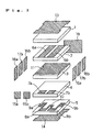
- Figure 1 is an exploded perspective view of a dielectric laminated filter according to one embodiment of this invention.
- Figure 2 is a perspective view of the dielectric laminated filter according to this embodiment (simply referred to as a "laminated body").
- Figure 3 shows an equivalent circuit of the dielectric laminated filter according to this embodiment.
- Reference numerals 6a and 6b indicate first strip line electrodes corresponding to first resonance electrodes according to this invention.
- the first strip line electrodes 6a and 6b are formed on the top surface of the dielectric sheet 2, extend from one side to the other, and are disposed in parallel to each other.
- Reference numerals 7a and 7b indicate second strip line electrodes corresponding to second resonance electrodes according to this invention, are formed on the top surface of the dielectric sheet 4, and extend from one side to the other of the dielectric sheet 4.
- Reference numerals 8a and 8b denote notch capacitance electrodes, 9a and 9b are I/O line electrodes, and 10 is a coupling line electrode. All these electrodes are formed on the top surface of the dielectric sheet 5.
- the notch capacitance electrodes 8a and 8b are formed opposite to the second strip line electrodes 7a and 7b.
- the I/O line electrodes 9a and 9b and the coupling line electrode 10 are formed in positions such that they are not opposed to the second strip line electrodes 7a and 7b.
- One end of the I/O line electrode 9a and one end of the coupling line electrode 10 are connected to the notch capacitance electrode 8a, and one end of the I/O line electrode 9b and the other end of the coupling line electrode 10 are connected to the notch capacity electrode 8b.
- Reference numeral 11 denotes a first shield electrode formed on the top surface of the dielectric sheet 3.
- these inner electrodes formed in the internal layers of the laminated body have electrode patterns printed thereon using metallic paste such as silver, copper, or gold having a high conductivity.
- 12 is the laminated body formed by laminating the dielectric sheets 5, 4, 3, 2, and 1 in this order, pressing them, and simultaneously sintering each dielectric sheet and each inner electrode.
- a plurality of dielectric laminated filters may be simultaneously manufactured from the same laminated body.
- a cutting process for cutting the laminated body into a plurality of laminated body pieces is required between the pressing process and the sintering process. These cut laminated body pieces correspond to the dielectric laminated filter.
- 13 is a second shield electrode
- 14 is a third shield electrode, and these electrodes are formed almost all over the top and the bottom surfaces of the laminated body 12, respectively.
- Reference numerals 15a and 15b are third strip line electrodes corresponding to third resonance electrodes according to this invention.
- the third strip line electrodes 15a and 15b are formed on one of the outer circumferential sides of the laminated body 12.
- the third strip line electrode 15a is connected to one end of the first strip line electrode 6a and one end of the second strip line electrode 7a.
- the third strip line electrode 15b is connected to one end of the first strip line electrode 6b and one end of the second strip line electrode 7b.
- Reference numerals 16a and 16b are connection electrodes formed on the two opposite outer circumferential sides of the laminated body 12 and connected to each of the shield electrodes 11, 13, and 14.
- Reference numerals 17a and 17b are I/O electrodes formed on the two outer circumferential sides of the laminated body 12.
- the I/O electrode 17a is connected to the other end of the I/O line electrode 9a and the I/O electrode 17b is connected to the other end of the I/O line electrode 9b.
- Reference numeral 18 is a ground terminal formed on one of the outer circumferential sides of the laminated body 12 and connected to the other end of each of the shield electrodes 11, 13, and 14 and the other ends of the first strip line electrodes 6a and 6b.
- the outer electrodes formed on the external surfaces of the laminated body are formed by printing or plating electrode patterns using metallic paste such as silver, copper, or gold having a high conductivity.
- the first dielectric laminated block according to this invention corresponds to a block including the dielectric sheets 1 and 2.
- the second dielectric laminated block according to this invention corresponds to a block including the dielectric sheets 3, 4, and 5.
- the dielectric laminated filter of this configuration is further described with reference to Figures 1, 2, and 3.
- the other ends of the first strip line electrodes 6a and 6b are grounded via the ground electrode 18 to constitute tip shorting strip line resonators 21a and 21b that use the other ends of the second strip line electrodes 7a and 7b as open ends.
- the notch capacitance electrodes 8a and 8b are formed opposite to the second strip line electrodes 7a and 7b to constitute the notch capacity elements 12a and 12b.
- the I/O line electrodes 9a and 9b and the coupling line electrode 10 act as coupling elements for distributed constant lines.
- the tip shorting strip line resonators 21a and 21b are connected in parallel via the notch capacity elements 20a and 20b as shown in the equivalent circuit diagram in Figure 3. This allows a band elimination filter using the I/O electrodes 17a and 17b as I/O terminals to be provided.
- this embodiment can laminate via the first shield electrode 11, the first dielectric laminated block including the first strip line electrodes 6a and 6b and the second dielectric laminated block including the second strip line electrodes 7a and 7b and coupling elements in order to prevent the unwanted electromagnetic coupling between the first strip line electrodes 6a and 6b and the I/O line electrodes 9a and 9b acting as the coupling elements and between the first strip line electrodes 6a and 6b and the coupling line electrode 10.
- the important point of this embodiment is the use of the structure in which the tip shorting strip line resonators 21a and 21b use the other ends of the second strip line electrodes 7a and 7b as open ends.
- This structure causes a field distribution to dominate in the second strip line electrodes, thereby allowing the magnetic coupling within the second dielectric laminated block to be neglected.
- the field coupling between the second strip line electrodes 7a and 7b and the notch capacitance electrodes 8a and 8b is used to form the notch capacity elements 20a and 20b (see Figure 3).
- the unwanted field coupling with the second strip line electrodes 7a and 7b can be reduced to a negligible magnitude.
- the unwanted field coupling between the resonators (that is, the tip shorting strip line resonators 21a and 21b) and the I/O lines (that is, the I/O line electrodes 9a and 9b) and between the resonators and the coupling element (that is, the coupling line electrode 10) can be reduced to a negligible magnitude, thereby enabling easy design and providing a good band elimination filter characteristic.
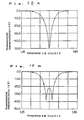
- Figures 18A to 18F show the transmission characteristic of a band elimination filter in which two strip line resonators are connected in parallel using a coupling line.
- Figure 18A is a graph showing a transmission characteristic obtained when the coupling line has an impedance of 50 ⁇ and a line length of a quarter wavelength at 1.5 GHz if there is no electromagnetic coupling between the resonators.
- Figure 18B is a graph that is the same as Figure 27A except that the resonance frequency is offset.
- Figure 18C is a graph that is the same as Figure 27B except that the coupling line length is a one-eighth wavelength at 1.5 GHz.
- Figure 18D is a graph that is the same as Figure 27A except that there is electromagnetic coupling between the resonators.
- Figure 18E is a graph that is the same as Figure 27D except that the coupling line length is a one-eighth wavelength at 1.5 GHz.
- Figure 18F is a graph that is the same as Figure 27E except that the gap between the resonators is expanded to reduce the electromagnetic coupling.
- Insertion losses can be reduced in a pass band 402 used to obtain a desired attenuation band 401 and attenuation amount.
- the attenuation band 401 can be expanded without providing a multi-stage filter, thereby reducing the size of the filter and losses (increasing the performance).
- the electromagnetic coupling between the resonators can be combined together as shown in Figure 18F to achieve an elliptic function characteristic with a steep attenuation characteristic curve.
- coupling elements can be provided which have an impedance and a wavelength that cannot be configured only by the coupling line electrode 10 due to a geometrical constraint.
- this embodiment has between the strip line electrodes 6a and 6b no earth electrode such as that described in the conventional dielectric laminated filter.
- An electromagnetic coupling prevention member according to this invention corresponds to the earth electrode.
- the thickness of the dielectric sheet 4 can be reduced to reduce the area of the second strip line electrodes 7a and 7b and notch capacitance electrodes 8a and 8b used to constitute the desired notch capacity elements 20a and 20b in order to increase the area used to form the coupling element without disposing it opposite to the second strip line electrodes 7a and 7b, thereby further increasing the degree of freedom in design.
- the wavelength of the resonators can be increased without increasing the size of the laminated body, thereby reducing the size of the tip shorting strip line resonators 21a and 21b.
- filter characteristics can be adjusted by forming the third strip line electrodes 15a and 15b of outer electrodes. That is, a trimming grinder or the like can be used to trim the third strip line electrodes 15a and 15b to adjust the interval between the electrodes in order to vary the electromagnetic coupling between the third strip line electrodes 15a and 15b, thereby allowing the attenuation band width within the band elimination filter characteristics to be adjusted.
- connection electrodes 16a and 16b By forming the connection electrodes 16a and 16b at the respective ends of the two opposite outer circumferential sides of the laminated body 12 and connecting the connection electrodes to each of the shield electrodes 11, 13, and 14, the same potential can be provided between the shield electrodes with a constant potential distribution maintained within each shield electrode, thereby providing stable filter characteristics with excellent shielding. These effects are significant at a frequency of more than 1 GHz.
- a dielectric laminated filter according to this embodiment is described below with reference to the drawings.
- the structure of the dielectric laminated filter according to this embodiment is almost the same as that in the first embodiment except that the first and the second dielectric laminated blocks are formed of dielectric sheets of different dielectric constants.
- the dielectric constant of the dielectric sheets 1 and 2 differs from that of the dielectric sheets 3, 4, and 5.
- this embodiment not only has the same effects as the first embodiment but, compared to the first embodiment, can also reduce the unwanted electromagnetic coupling between the resonators and the I/O lines and between the resonators and the coupling element without increasing the size of the dielectric laminated filter by making the dielectric sheets 1 and 2 of a material of a low dielectric constant and making the dielectric sheets 3, 4, and 5 of a material of a high dielectric constant.
- the dielectric sheets 2 and 3 of different materials can be laminated via the first shield electrode to reduce changes in material caused by the chemical binding between different materials, thereby enabling different materials to be laminated easily, compared to the prior art.
- Figure 4 is an exploded perspective view of a dielectric laminated filter according to this embodiment of the invention.
- Figure 5 is a perspective view of a dielectric body according to this embodiment.
- Figure 6 shows an equivalent circuit of the dielectric laminated filter according to this embodiment.
- this dielectric laminated filter is the same as that in the first embodiment except for the following points.
- the second and the third shield electrodes 13 and 14 are formed as inner electrode and dielectric sheets 41 and 42 are laminated on the top and the bottom surfaces to form a laminated body 45.
- the third strip line electrodes 15a and 15b are formed to extend up to the top surface of the dielectric sheet 41.
- this embodiment not only has the same effects as the first embodiment but can also reduce the resonance frequency of the tip shorting strip line resonators 21a and 21b (see Figure 6) by extending the third strip line electrodes 15a and 15b up to the top surface of the dielectric sheet 41 to form ground capacity elements 44a and 44b between the third strip line electrodes 15a and 15b and the second shield electrode 13. Consequently, the length of the tip shorting strip line resonators 21a and 21b, that is, the wavelength can be reduced.
- the capacity (capacitance) of the ground capacity elements 44a and 44b can be varied to adjust the resonance frequency of the tip shorting strip line resonators 21a and 21b.
- This adjustment can be normally provided in the middle of a manufacturing process to absorb the dispersion of dielectric sheets and electrode patterns, thereby improving the yield.
- connection electrodes 16a and 16b, the I/O electrodes 17a and 17b, and the ground electrode 18 are extended up to the top surface of the dielectric sheet 41 and the bottom surface of the dielectric sheet 42 and if the laminated body is mounted on a substrate by reflow soldering, the solder can be more effectively attached to each electrode surface and firmly mounted, thereby improving the reliability of mounting.
- Figure 16 is a graph showing the frequency characteristic of a dielectric laminated filter experimentally manufactured according to this embodiment.
- the electromagnetic coupling between the resonators and the coupling line electrode 10 were, as described above, appropriately combined together to achieve an elliptic function characteristic 160 such as that shown in Figure 23.
- Figure 7 is an exploded perspective view of a dielectric laminated filter according to this embodiment of the invention.
- Figure 8 is a perspective view of a dielectric body according to this embodiment.
- Figure 9 shows an equivalent circuit of the dielectric laminated filter according to this embodiment.
- this dielectric laminated filter is the same as that in the first embodiment except for the following points.
- the second shield electrode 13 is formed all over the surface of the laminated body 12.
- the ground electrode 18 is formed all over one of the outer circumferential sides of the laminated body 12.
- a fourth shield electrode 71 is formed all over two opposite sides of the dielectric sheets 1 and 2 to connect the connection electrodes 16a and 16b to the fourth shield electrode 71.
- the line width of the second strip line electrodes 7a and 7b is formed to be larger than that of the first strip line electrodes 6a and 6b.
- this embodiment not only has the same ef fects as the first embodiment but also improves the shielding capability of the first strip line electrodes 6a and 6b with a large magnetic density to reduce radiation losses because the shield electrode is formed all over the top surface and all the outer circumferential sides of the first dielectric laminated block other than the one on which the third strip line electrodes 15a and 15b are formed, the first dielectric laminated block including the dielectric sheets 1 and 2 and the first strip line electrodes 6a and 6b.
- the unloaded Q of the tip shorting strip line resonators 21a and 21b can be improved to realize a high performance dielectric laminated filter.
- the line width of the second strip line electrodes 7a and 7b is formed to be larger than that of the first strip line electrodes 6a and 6b in order to cause the impedance of the tip shorting strip line resonators 21a and 21b to be abruptly varied like a step. This provides SIR resonators to enable the resonance frequency and the length of the resonators to be reduced in order to realize a small dielectric laminated filter.
- Figure 10 is an exploded perspective view of a dielectric laminated filter according to this embodiment of the invention.
- Figure 11 is a perspective view of a dielectric body according to this embodiment.
- Figure 12 shows an equivalent circuit of the dielectric laminated filter according to this embodiment.
- FIG. 10 and 11 The structure in Figures 10 and 11 is the same as that in the first embodiment except for the following points.
- open stubs 31a and 31b are formed on the top surface of the dielectric sheet 5 to connect the I/O line electrodes 9a and 9b in parallel.
- the second dielectric block has a smaller thickness than the first dielectric block.
- this embodiment not only has the same effects as the first embodiment but can also size the open stubs 31a and 31b so as to have a length equal to a quarter wavelength at frequencies double and triple the fundamental pass band to form an attenuating pole at these frequencies.
- This attenuating pole is effective in attenuating a second and a third harmonic bands and enables an attenuating pole to be formed without affecting the characteristics of the fundamental frequency band.
- the thickness of the second dielectric block (corresponding to the laminated portion including the dielectric sheets 3, 4, and 5) can be reduced below that of the first dielectric block (corresponding to the laminated portion including the dielectric sheets 1 and 2) to reduce the impedance of the second strip line electrodes 7a and 7b below that of the first strip line electrodes 6a and 6b, thereby enabling the impedance of the tip shorting strip line resonators 21a and 21b to be abruptly varied like a step. That is, SIR resonators can be provided to reduce the resonance frequency and thus the length of the resonators.
- this embodiment can attenuate high-order harmonic bands without the need to add an LPF, thereby reducing the size and losses of the multi-functional filter. Due to its ability to reduce the length of the resonators, this embodiment can realize a much smaller dielectric laminated filter.
- the communication apparatus comprises, for example, a receipt means for receiving a radio signal from a source; a signal processing means comprising the dielectric laminated filter described in any of the above embodiments to extract a predetermined portion from the received signal and processing it; an output means for outputting the processed signal to a speaker, and a signalling means for issuing a signal to the source.
- the signalling means can be omitted from the communication apparatus.
- the above embodiments can provide a small high-performance dielectric laminated filter that can be designed easily and that enables the resonance frequency of the filter and the electromagnetic coupling between resonators to be adjusted during a manufacturing process.
Landscapes
- Physics & Mathematics (AREA)
- Electromagnetism (AREA)
- Control Of Motors That Do Not Use Commutators (AREA)
Claims (11)
- Un filtre stratifié diélectrique à élimination de bande, comprenant :Caractérisé en ce queun premier bloc stratifié diélectrique dans lequel une pluralité de feuilles diélectriques (1, 2) sont stratifiées,une pluralité de premières électrodes de ligne à microbande (6a, 6b), formées sur une couche interne (2) dudit premier bloc stratifié diélectrique,un second bloc stratifié diélectrique dans lequel une pluralité de feuilles diélectriques (3, 4, 5) sont stratifiées,une pluralité de secondes électrodes de ligne à microbande (7a, 7b) formées sur une couche interne (4) dudit second bloc stratifié diélectrique,au moins deux électrodes de ligne d'entrée/sortie (9a, 9b) formées sur une autre couche interne (5) dudit second bloc stratifié,une électrode de blindage (11) formée entre ledit premier bloc stratifié diélectrique et ledit second bloc stratifié diélectrique,
Ledit filtre stratifié diélectrique à élimination de bande comprend, en outre, au moins une électrode de ligne de couplage (10) et une pluralité d'électrodes capacitives coupe-bande à bande étroite (8a, 8b) formées sur l'autre couche interne (5) dudit second bloc stratifié, dans lequel ladite électrode de ligne de couplage (10), lesdites électrodes capacitives coupe-bande à bande étroite (8a, 8b) et lesdites électrodes de ligne d'entrée/sortie (8a, 8b) sont connectées électriquement en séries,
lesdites premières électrodes de ligne à microbande respectives (6a, 6b) et lesdites secondes électrodes de ligne à microbande respectives (7a, 7b) sont connectées pour former une pluralité de résonateurs,
lesdites secondes électrodes de ligne à microbande respectives (7a, 7b) et lesdites électrodes capacitives coupe-bande à bande étroite respectives (8a, 8b) sont opposées pour former une pluralité d'éléments capacitifs coupe-bande à bande étroite (20a, 20b), - Un filtre stratifié diélectrique à élimination de bande selon la revendication 1, comprenant, en outre, une pluralité d'électrodes de connexion (15a, 15b), dans lequel lesdites électrodes de connexion (15a, 15b) sont formées sur une surface latérale et connectent lesdites premières électrodes de ligne à microbande (6a, 6b) et lesdites secondes lignes à microbande respectives (7a, 7b) électriquement.
- Un filtre stratifié diélectrique à élimination de bande selon la revendication 2, comprenant, en outre, des électrodes de blindage (13, 14, 18) qui recouvrent presque totalement la surface externe sauf la surface sur laquelle lesdites électrodes de connexion (15a, 15b) sont formées.
- Un filtre stratifié diélectrique à élimination de bande selon l'une quelconque des revendications 1 à 3, dans lequel lesdites secondes électrodes de ligne à microbande (7a, 7b) présentent une largeur plus grande que la largeur desdites premières électrodes de ligne à microbande (6a, 6b).
- Un filtre stratifié diélectrique à élimination de bande selon l'une quelconque des revendications 1 à 4, dans lequel lesdits premier et second blocs stratifiés diélectriques présentent des épaisseurs différentes.
- Un filtre stratifié diélectrique à élimination de bande selon l'une quelconque des revendications 1 à 5, dans lequel lesdits premier et second bloc diélectriques sont formés desdites feuilles diélectriques de constantes diélectriques différentes.
- Un filtre stratifié diélectrique à élimination de bande selon l'une quelconque des revendications 1 à 6, incluant des tronçons ouverts (31a, 31b) connectés auxdites électrodes de ligne d'entrée/sortie (9a, 9b) pour atténuer les bandes d'harmoniques d'ordre plus élevé.
- Un filtre stratifié diélectrique à élimination de bande selon l'une quelconque des revendications 1 à 7, dans lequel les fréquences de résonance desdits résonateurs sont décalées les unes par rapport aux autres.
- Un filtre stratifié diélectrique à élimination de bande selon l'une quelconque des revendications 1 à 8, dans lequel ladite électrode de blindage (11) couvre la totalité desdites premières électrodes de ligne à microbande (6a, 6b) sauf pour les extrémités ouvertes desdites premières électrodes de ligne à microbande (6a, 6b) de manière telle que ladite électrode de blindage (11) empêche un couplage entre lesdites premières électrodes de ligne à microbande (6a, 6b) et ladite électrode de ligne de couplage (10) et entre lesdites premières électrodes de ligne à microbande (6a, 6b) et lesdites électrodes de ligne d'entrée/sortie (9a, 9b), et les extrémités ouvertes desdites secondes électrodes de ligne à microbande respectives (7a, 7b), et lesdites électrodes capacitives coupe-bande à bande étroite respectives (8a, 8b) sont opposées pour former une pluralité d'éléments capacitifs coupe-bande à bande étroite (20a, 20b)
- Un filtre stratifié diélectrique à élimination de bande selon la revendication 2 ou 3, dans lequel le matériau des électrodes (6a, 6b, 7a, 7b) formé dans les couches internes du filtre stratifié diélectrique à élimination de bande est différent de celui des électrodes (15a, 15b) formées à l'extérieur dudit filtre stratifié diélectrique à élimination de bande.
- Un appareil de communication comprenant :un moyen de récepteur pour recevoir un signal ;un moyen de traitement du signal utilisant un filtre stratifié diélectrique à élimination de bande en conformité avec l'une quelconque des revendications 1 à 10, etun moyen de sortie pour sortir un signal traité.
Priority Applications (1)
| Application Number | Priority Date | Filing Date | Title |
|---|---|---|---|
| EP02014860A EP1265312B1 (fr) | 1996-10-18 | 1997-10-16 | Filtre diélectrique stratifié éliminateur de bande avec couplage électromagnétique entre résonateurs |
Applications Claiming Priority (3)
| Application Number | Priority Date | Filing Date | Title |
|---|---|---|---|
| JP276102/96 | 1996-10-18 | ||
| JP27610296 | 1996-10-18 | ||
| JP27610296 | 1996-10-18 |
Related Child Applications (1)
| Application Number | Title | Priority Date | Filing Date |
|---|---|---|---|
| EP02014860A Division EP1265312B1 (fr) | 1996-10-18 | 1997-10-16 | Filtre diélectrique stratifié éliminateur de bande avec couplage électromagnétique entre résonateurs |
Publications (3)
| Publication Number | Publication Date |
|---|---|
| EP0837517A2 EP0837517A2 (fr) | 1998-04-22 |
| EP0837517A3 EP0837517A3 (fr) | 2000-08-09 |
| EP0837517B1 true EP0837517B1 (fr) | 2004-01-28 |
Family
ID=17564835
Family Applications (2)
| Application Number | Title | Priority Date | Filing Date |
|---|---|---|---|
| EP97117967A Expired - Lifetime EP0837517B1 (fr) | 1996-10-18 | 1997-10-16 | Filtre diélectrique statifié et dispositif de communication |
| EP02014860A Expired - Lifetime EP1265312B1 (fr) | 1996-10-18 | 1997-10-16 | Filtre diélectrique stratifié éliminateur de bande avec couplage électromagnétique entre résonateurs |
Family Applications After (1)
| Application Number | Title | Priority Date | Filing Date |
|---|---|---|---|
| EP02014860A Expired - Lifetime EP1265312B1 (fr) | 1996-10-18 | 1997-10-16 | Filtre diélectrique stratifié éliminateur de bande avec couplage électromagnétique entre résonateurs |
Country Status (3)
| Country | Link |
|---|---|
| US (1) | US6140891A (fr) |
| EP (2) | EP0837517B1 (fr) |
| DE (2) | DE69736617T2 (fr) |
Families Citing this family (22)
| Publication number | Priority date | Publication date | Assignee | Title |
|---|---|---|---|---|
| JPH11205006A (ja) * | 1998-01-20 | 1999-07-30 | Matsushita Electric Ind Co Ltd | 積層フィルタ |
| EP0998036B1 (fr) * | 1998-03-17 | 2003-11-05 | Matsushita Electric Industrial Co., Ltd. | Filtre de multiplexage/derivation |
| US6379805B1 (en) * | 1999-01-22 | 2002-04-30 | Ngk Insulators, Ltd. | Low temperature-fired porcelain articles and electronic parts including such porcelain articles |
| EP1067618B1 (fr) * | 1999-07-08 | 2007-12-12 | Matsushita Electric Industrial Co., Ltd. | Filtre stratifié, duplexeur et dispositif de communication mobile l' utilisant |
| US6603372B1 (en) | 1999-11-29 | 2003-08-05 | Matsushita Electric Industrial Co., Ltd. | Laminated notch filter and cellular phone using the same |
| US6529096B2 (en) | 2000-05-30 | 2003-03-04 | Matsushita Electric Industrial Co., Ltd. | Dielectric filter, antenna duplexer, and communications appliance |
| DE10123369A1 (de) * | 2001-05-14 | 2002-12-05 | Infineon Technologies Ag | Filteranordnung für, symmetrische und unsymmetrische Leitungssysteme |
| US7023301B2 (en) * | 2001-05-16 | 2006-04-04 | Matsushita Electric Industrial Co., Ltd. | Laminated filter with a single shield conductor, integrated device, and communication apparatus |
| DE10217387B4 (de) * | 2002-04-18 | 2018-04-12 | Snaptrack, Inc. | Elektrisches Anpassungsnetzwerk mit einer Transformationsleitung |
| CN1459811A (zh) * | 2002-05-22 | 2003-12-03 | 松下电器产业株式会社 | 陶瓷层压器件、通信设备和制造陶瓷层压器件的方法 |
| US7012481B2 (en) * | 2002-10-04 | 2006-03-14 | Matsushita Electric Industrial Co., Ltd. | Duplexer, and laminate-type high-frequency device and communication equipment using the same |
| JP4111222B2 (ja) * | 2003-07-22 | 2008-07-02 | 株式会社村田製作所 | 表面実装型部品 |
| DE10348722B4 (de) | 2003-10-16 | 2013-02-07 | Epcos Ag | Elektrisches Anpassungsnetzwerk mit einer Transformationsleitung |
| US20070120627A1 (en) * | 2005-11-28 | 2007-05-31 | Kundu Arun C | Bandpass filter with multiple attenuation poles |
| JP2008099060A (ja) * | 2006-10-13 | 2008-04-24 | Taiyo Yuden Co Ltd | 積層型誘電体帯域通過フィルタ |
| JP4438864B2 (ja) * | 2007-12-28 | 2010-03-24 | 株式会社村田製作所 | 基板及びこれを備えた電子装置 |
| DE102008045346B4 (de) | 2008-09-01 | 2018-06-07 | Snaptrack Inc. | Duplexer und Verfahren zum Erhöhen der Isolation zwischen zwei Filtern |
| US8680952B2 (en) * | 2008-12-30 | 2014-03-25 | Tdk Corporation | Bandpass filter with dual band response |
| US8547188B2 (en) * | 2009-02-23 | 2013-10-01 | Tdk Corporation | Filter with integrated loading capacitors |
| US20170245361A1 (en) * | 2016-01-06 | 2017-08-24 | Nokomis, Inc. | Electronic device and methods to customize electronic device electromagnetic emissions |
| CN110380169B (zh) * | 2019-06-27 | 2020-11-13 | 南京理工大学 | 一种具有改善带阻特性的陷波频率可调超宽带滤波器 |
| CN113506962B (zh) * | 2021-08-11 | 2024-03-12 | 中国电子科技集团公司第二十六研究所 | 陷波可调谐振结构及小型片式介质滤波器 |
Family Cites Families (14)
| Publication number | Priority date | Publication date | Assignee | Title |
|---|---|---|---|---|
| US5191304A (en) * | 1990-03-02 | 1993-03-02 | Orion Industries, Inc. | Bandstop filter having symmetrically altered or compensated quarter wavelength transmission line sections |
| JP2502824B2 (ja) * | 1991-03-13 | 1996-05-29 | 松下電器産業株式会社 | 平面型誘電体フィルタ |
| JPH05218705A (ja) * | 1992-02-05 | 1993-08-27 | Ngk Insulators Ltd | 積層型帯域除去フィルター |
| JP2957041B2 (ja) * | 1992-02-28 | 1999-10-04 | 日本碍子株式会社 | 積層型誘電体フィルタ |
| JPH0645803A (ja) * | 1992-07-22 | 1994-02-18 | Fujitsu Ltd | ストリップラインフィルタおよびフィルタ装置 |
| JP2860018B2 (ja) * | 1992-09-16 | 1999-02-24 | 日本碍子株式会社 | 誘電体フィルタ |
| JPH06268410A (ja) * | 1993-03-12 | 1994-09-22 | Ngk Insulators Ltd | 積層型帯域除去フィルタ |
| JPH06268411A (ja) * | 1993-03-12 | 1994-09-22 | Ngk Insulators Ltd | 積層型帯域除去フィルタ |
| US5479141A (en) * | 1993-03-25 | 1995-12-26 | Matsushita Electric Industrial Co., Ltd. | Laminated dielectric resonator and dielectric filter |
| JP3115149B2 (ja) * | 1993-03-31 | 2000-12-04 | 日本碍子株式会社 | 積層型誘電体フィルタ |
| JPH0758506A (ja) * | 1993-08-09 | 1995-03-03 | Oki Electric Ind Co Ltd | Lc型誘電体フィルタ、およびこれを用いた空中線共用器 |
| EP0917235B1 (fr) * | 1993-08-24 | 2003-01-22 | Matsushita Electric Industrial Co., Ltd. | Duplexeur diélectrique stratifié d' antenne |
| JP3351102B2 (ja) * | 1994-06-14 | 2002-11-25 | 株式会社村田製作所 | 共振器 |
| JPH0897603A (ja) * | 1994-09-29 | 1996-04-12 | Kyocera Corp | 積層型誘電体フィルタ |
-
1997
- 1997-10-16 EP EP97117967A patent/EP0837517B1/fr not_active Expired - Lifetime
- 1997-10-16 DE DE69736617T patent/DE69736617T2/de not_active Expired - Lifetime
- 1997-10-16 EP EP02014860A patent/EP1265312B1/fr not_active Expired - Lifetime
- 1997-10-16 DE DE69727353T patent/DE69727353T2/de not_active Expired - Lifetime
- 1997-10-20 US US08/954,381 patent/US6140891A/en not_active Expired - Lifetime
Also Published As
| Publication number | Publication date |
|---|---|
| EP0837517A2 (fr) | 1998-04-22 |
| EP1265312A3 (fr) | 2003-06-25 |
| EP0837517A3 (fr) | 2000-08-09 |
| US6140891A (en) | 2000-10-31 |
| EP1265312A2 (fr) | 2002-12-11 |
| DE69727353T2 (de) | 2004-07-01 |
| DE69736617T2 (de) | 2007-01-04 |
| DE69736617D1 (de) | 2006-10-12 |
| DE69727353D1 (de) | 2004-03-04 |
| EP1265312B1 (fr) | 2006-08-30 |
Similar Documents
| Publication | Publication Date | Title |
|---|---|---|
| EP0837517B1 (fr) | Filtre diélectrique statifié et dispositif de communication | |
| EP0617478B1 (fr) | Résonateur diélectrique stratifié et filtre diélectrique | |
| EP1742354B1 (fr) | Filtre passe-bande multicouche | |
| EP0641035B1 (fr) | Duplexeur stratifié d'antenne et filtre diélectrique | |
| US6075491A (en) | Chip antenna and mobile communication apparatus using same | |
| US6411178B1 (en) | Multi-layer composite electronic component | |
| EP0336255B1 (fr) | Filtre monté sur la surface, avec une connexion sous forme de ligne de transmission intégrée | |
| EP0997973B1 (fr) | Antenne à filtre et appareil radio utilisant cette antenne | |
| KR100456262B1 (ko) | Lc 필터 회로, 적층형 lc 복합부품, 멀티플렉서 및무선 통신 장치 | |
| US7663455B2 (en) | Band-pass filter element and high frequency module | |
| JPWO2002067379A1 (ja) | フィルタ内蔵アンテナ | |
| JP3319418B2 (ja) | 高周波回路装置、アンテナ共用器及び通信機装置 | |
| JP2752048B2 (ja) | 対称型ストリップライン共振器 | |
| US6529096B2 (en) | Dielectric filter, antenna duplexer, and communications appliance | |
| JP2001217607A (ja) | アンテナ装置 | |
| Nishikawa | RF front end circuit components miniaturized using dielectric resonators for cellular portable telephones | |
| US5489881A (en) | Stripline resonator filter including cooperative conducting cap and film | |
| US5994978A (en) | Partially interdigitated combline ceramic filter | |
| US6356244B1 (en) | Antenna device | |
| US20040066256A1 (en) | Duplexer, and laminate-type high-frequency device and communication equipment using the same | |
| WO1988001104A1 (fr) | Filtre a resonateurs multiples pouvant etre monte sur un element exterieur | |
| US6222430B1 (en) | Dielectric filter | |
| JPH10178302A (ja) | 誘電体積層フィルタ及び通信装置 | |
| JP3464820B2 (ja) | 誘電体積層共振器および誘電体フィルタ | |
| JP3676885B2 (ja) | チップ型積層フィルタ |
Legal Events
| Date | Code | Title | Description |
|---|---|---|---|
| PUAI | Public reference made under article 153(3) epc to a published international application that has entered the european phase |
Free format text: ORIGINAL CODE: 0009012 |
|
| AK | Designated contracting states |
Kind code of ref document: A2 Designated state(s): DE FR GB |
|
| PUAL | Search report despatched |
Free format text: ORIGINAL CODE: 0009013 |
|
| AK | Designated contracting states |
Kind code of ref document: A3 Designated state(s): AT BE CH DE DK ES FI FR GB GR IE IT LI LU MC NL PT SE |
|
| 17P | Request for examination filed |
Effective date: 20000808 |
|
| AKX | Designation fees paid |
Free format text: DE FR GB |
|
| 17Q | First examination report despatched |
Effective date: 20020124 |
|
| GRAP | Despatch of communication of intention to grant a patent |
Free format text: ORIGINAL CODE: EPIDOSNIGR1 |
|
| GRAS | Grant fee paid |
Free format text: ORIGINAL CODE: EPIDOSNIGR3 |
|
| GRAA | (expected) grant |
Free format text: ORIGINAL CODE: 0009210 |
|
| AK | Designated contracting states |
Kind code of ref document: B1 Designated state(s): DE FR GB |
|
| REG | Reference to a national code |
Ref country code: GB Ref legal event code: FG4D |
|
| REF | Corresponds to: |
Ref document number: 69727353 Country of ref document: DE Date of ref document: 20040304 Kind code of ref document: P |
|
| ET | Fr: translation filed | ||
| PLBE | No opposition filed within time limit |
Free format text: ORIGINAL CODE: 0009261 |
|
| STAA | Information on the status of an ep patent application or granted ep patent |
Free format text: STATUS: NO OPPOSITION FILED WITHIN TIME LIMIT |
|
| 26N | No opposition filed |
Effective date: 20041029 |
|
| PGFP | Annual fee paid to national office [announced via postgrant information from national office to epo] |
Ref country code: GB Payment date: 20141015 Year of fee payment: 18 Ref country code: FR Payment date: 20141008 Year of fee payment: 18 Ref country code: DE Payment date: 20141007 Year of fee payment: 18 |
|
| REG | Reference to a national code |
Ref country code: DE Ref legal event code: R119 Ref document number: 69727353 Country of ref document: DE |
|
| GBPC | Gb: european patent ceased through non-payment of renewal fee |
Effective date: 20151016 |
|
| PG25 | Lapsed in a contracting state [announced via postgrant information from national office to epo] |
Ref country code: GB Free format text: LAPSE BECAUSE OF NON-PAYMENT OF DUE FEES Effective date: 20151016 Ref country code: DE Free format text: LAPSE BECAUSE OF NON-PAYMENT OF DUE FEES Effective date: 20160503 |
|
| REG | Reference to a national code |
Ref country code: FR Ref legal event code: ST Effective date: 20160630 |
|
| PG25 | Lapsed in a contracting state [announced via postgrant information from national office to epo] |
Ref country code: FR Free format text: LAPSE BECAUSE OF NON-PAYMENT OF DUE FEES Effective date: 20151102 |