EP0845779B1 - Speicherung und Übertragung von 1-bit Daten - Google Patents
Speicherung und Übertragung von 1-bit Daten Download PDFInfo
- Publication number
- EP0845779B1 EP0845779B1 EP97307995A EP97307995A EP0845779B1 EP 0845779 B1 EP0845779 B1 EP 0845779B1 EP 97307995 A EP97307995 A EP 97307995A EP 97307995 A EP97307995 A EP 97307995A EP 0845779 B1 EP0845779 B1 EP 0845779B1
- Authority
- EP
- European Patent Office
- Prior art keywords
- bit
- signal
- input
- digital signal
- data bits
- Prior art date
- Legal status (The legal status is an assumption and is not a legal conclusion. Google has not performed a legal analysis and makes no representation as to the accuracy of the status listed.)
- Expired - Lifetime
Links
- 230000005540 biological transmission Effects 0.000 title claims description 18
- 230000005236 sound signal Effects 0.000 claims description 11
- 238000000034 method Methods 0.000 claims description 4
- 230000000694 effects Effects 0.000 description 2
- 238000005070 sampling Methods 0.000 description 2
- 230000003595 spectral effect Effects 0.000 description 2
- 230000005856 abnormality Effects 0.000 description 1
- 230000000295 complement effect Effects 0.000 description 1
- 238000001514 detection method Methods 0.000 description 1
- 239000013307 optical fiber Substances 0.000 description 1
- 238000003825 pressing Methods 0.000 description 1
- 230000001131 transforming effect Effects 0.000 description 1
Images
Classifications
-
- G—PHYSICS
- G11—INFORMATION STORAGE
- G11B—INFORMATION STORAGE BASED ON RELATIVE MOVEMENT BETWEEN RECORD CARRIER AND TRANSDUCER
- G11B20/00—Signal processing not specific to the method of recording or reproducing; Circuits therefor
- G11B20/10—Digital recording or reproducing
- G11B20/10527—Audio or video recording; Data buffering arrangements
-
- G—PHYSICS
- G11—INFORMATION STORAGE
- G11B—INFORMATION STORAGE BASED ON RELATIVE MOVEMENT BETWEEN RECORD CARRIER AND TRANSDUCER
- G11B20/00—Signal processing not specific to the method of recording or reproducing; Circuits therefor
- G11B20/10—Digital recording or reproducing
- G11B20/12—Formatting, e.g. arrangement of data block or words on the record carriers
-
- G—PHYSICS
- G11—INFORMATION STORAGE
- G11B—INFORMATION STORAGE BASED ON RELATIVE MOVEMENT BETWEEN RECORD CARRIER AND TRANSDUCER
- G11B27/00—Editing; Indexing; Addressing; Timing or synchronising; Monitoring; Measuring tape travel
- G11B27/10—Indexing; Addressing; Timing or synchronising; Measuring tape travel
- G11B27/19—Indexing; Addressing; Timing or synchronising; Measuring tape travel by using information detectable on the record carrier
- G11B27/28—Indexing; Addressing; Timing or synchronising; Measuring tape travel by using information detectable on the record carrier by using information signals recorded by the same method as the main recording
- G11B27/32—Indexing; Addressing; Timing or synchronising; Measuring tape travel by using information detectable on the record carrier by using information signals recorded by the same method as the main recording on separate auxiliary tracks of the same or an auxiliary record carrier
- G11B27/322—Indexing; Addressing; Timing or synchronising; Measuring tape travel by using information detectable on the record carrier by using information signals recorded by the same method as the main recording on separate auxiliary tracks of the same or an auxiliary record carrier used signal is digitally coded
- G11B27/323—Time code signal, e.g. on a cue track as SMPTE- or EBU-time code
-
- H—ELECTRICITY
- H03—ELECTRONIC CIRCUITRY
- H03K—PULSE TECHNIQUE
- H03K19/00—Logic circuits, i.e. having at least two inputs acting on one output; Inverting circuits
- H03K19/20—Logic circuits, i.e. having at least two inputs acting on one output; Inverting circuits characterised by logic function, e.g. AND, OR, NOR, NOT circuits
- H03K19/21—EXCLUSIVE-OR circuits, i.e. giving output if input signal exists at only one input; COINCIDENCE circuits, i.e. giving output only if all input signals are identical
Definitions
- This invention relates to the storage and transmission of one-bit (or delta-sigma modulated) data, such as one-bit digital audio signals.
- a convenient way of storing one-bit digital audio signals with currently available equipment is to multiplex groups of bits of the one-bit signal into data words, and then to record the data words on conventional multi-bit PCM recording equipment.
- a one-bit signal at 64fs (where fs is, for example, 48 kHz) can be treated in this way by multiplexing 64 successive bits of the one-bit signal into 4 x 16-bit words, which can then be recorded on two stereo channels of a standard so-called AES/EBU digital audio recorder.
- GB 2 287 624-A describes an audio signal processing apparatus according to which a noise of maximum level can be prevented from being generated when an abnormality occurs in the transmission system by detecting when a sigma-delta modulated audio signal takes a fixed value for greater than a predetermined time interval and switching a quantised signal to a predetermined idling signal when such a detection is made.
- JP-A-63 094 718 describes a system that is operable to cancel an offset voltage by inverting the polarity of an output of a delta-sigma analogue to digital converter according to a clock signal having a frequency f3 that is much less than the sampling frequency f1.
- EP 0385 288 describes a system for the transmission of time-division multiplexed digital messages.
- Digital signals from a number of different communication channels are time-division multiplexed and in the event that a signal on one of the channels is missing, a bit stream of another channel is inverted and transmitted instead of the missing channel signal.
- the output signal has a constant binary 1/0 distribution.
- the 1/0 distribution is symmetrical with a high number of alternations.
- This invention provides apparatus for storing and/or transmitting a one-bit digital signal, the apparatus comprising:
- the invention addresses the above problems by inverting alternate of the data bits of the one-bit signal before they are recorded or transmitted, and then re-inverting those data bits on reception or reproduction.
- This provides a processing scheme which is transparent to the signals when they are properly received or reproduced.
- the alternate bit inversion built into the replay or reception side of the apparatus will generate a one-bit output signal having a subset of inverted bits, representing a lower level signal in the one-bit domain.
- alternate bits of the input signal are inverted and so the output during a mute would be alternate ones and zeroes - the one-bit equivalent of digital silence.
- This invention also provides apparatus for formatting a one-bit digital signal for storage and/or transmission, the apparatus comprising an inverter for inverting alternate data bits of an input one-bit digital signal, to generate a bit-inverted signal to be stored or transmitted.
- This invention also provides apparatus for receiving a one-bit digital signal after storage and/or transmission, the apparatus comprising an inverter for inverting alternate data bits of the received one-bit digital signal.
- This invention also provides a method of storing and/or transmitting a one-bit digital signal, the method comprising the successive steps of:
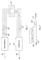
- a one-bit digital data recording system comprises a demultiplexer 10 for receiving an input one-bit digital audio signal 20, a data recorder 30 (in this case, a so-called AES/EBU standard digital audio recorder), and a multiplexer 40 for generating an output one-bit digital audio signal 50.
- Bit-inverters 60 and 70 are connected between the demultiplexer 10 and the data recorder 30 and between the data recorder 30 and the multiplexer 40.
- the input one-bit signal 20 comprises successive individual data bits: b 1 , b 2 , b 3 , b 4 , b 5 , b 6 , b 7 , ..., ... b 63 , b 64 , b 65 , b 66 , ...
- the AES/EBU recorder 30 is designed to record 16-bit data words (each representing a PCM audio sample) at a sampling rate of 48kHz.
- the demultiplexer 10 forms groups of the data bits of the one-bit input signal and passing them to the AES/EBU recorder 30 for recording as though they were 16-bit PCM data words.
- the one-bit digital audio signal has a data rate (bit rate) of 64fs, where fs is 48kHz, and so for each sample period of the 48kHz AES/EBU recorder, 64 bits of the one-bit digital audio signal must be multiplexed and recorded as data words. Therefore, four 16-bit data words are required to be formed for each 48kHz sample period.
- Four data words per sample period correspond to four audio channels being recorded on the AES/EBU data recorder. In fact, this can be configured as two stereo channels to accommodate the four data words per sample period.
- the two stereo channels are represented by pairs of signals 80, 90 in Figure 1 1 .
- bit streams each comprising alternate data bits from the input one-bit signal. Therefore, the bit streams would contain:
- Each of the two bit streams is then sub-divided to form the two channels of a respective stereo pair, for recording on the AES/EBU recorder. This is done by taking alternate groups of 16 adjacent bits and assigning them to one of the left and right channels of that stereo pair. So, using the notation established above, the following 16-bit data words would be generated for recording on the AES/EBU recorder 30:
- the inverters 60 invert the data bits of one of the stereo pairs before recording. Similar inverters 70 invert the same stereo pair when it is reproduced from the recorder 30. Because each stereo pair is formed from a respective bit stream, which in turn is formed of alternate bits of the input one-bit signal, the inverters 60 have the effect of inverting alternate bits of the input one-bit signal. These bits are then re-inverted on replay by the inverters 70 to reconstruct the bits of the input one-bit signal.
- the multiplexer 40 operates in a complementary manner to the demultiplexer 10, to convert replayed 16-bit data words into the one-bit signal b 1 , b 2 , b 3 , b 4 ...
- One advantage of this embodiment is that if there is an error which leads to a failure during replay on the AES/EBU recorder 30, that recorder will "mute" to a signal comprising successive digital zeroes. This is no problem in a PCM system, because a signal of all zeroes represents silence. However, in a one-bit signal, a signal of all zeroes represents a very loud noise indeed.
- the inverters 70 are operable to invert alternate bits output by the AES/EBU recorder (alternate in the sense that they become alternate within the one-bit signal output by the multiplexer 40), a mute signal is transformed into an output one-bit signal comprising alternate ones and zeroes.
- a signal of alternate ones and zeroes is a close representation of silence in a one-bit system.
- a mute signal may also be output and will be treated in the same way.
- the recorder 30 may be replaced by a transmission medium such as a cable, optical fibre or satellite link. If the transmission medium is disconnected or fails in any other way, or if it mutes through any transmission problems, then the inverters 70 have the same effect of transforming a PCM digital silence into a one-bit digital silence signal.
- a transmission medium such as a cable, optical fibre or satellite link.
- any inversion pattern which results in a silence signal having a substantially even distribution of ones and zeroes could perform the same function, and indeed there can be advantages in using an inversion pattern which inverts, perhaps, four bits at "random" positions within each 8-bit group of the input one-bit signal, to "spread out” the spectral energy of the "digital silence" signal.
- an inversion pattern which inverts, perhaps, four bits at "random" positions within each 8-bit group of the input one-bit signal, to "spread out” the spectral energy of the "digital silence” signal.
- Figure 2 schematically illustrates an example arrangement in which a generic bit inverter which could perform this function in place of the inverters 60 and 70.
- bit stream to be inverted is supplied on an input 100, and a bit-inverted bit stream is generated at an output 110.
- the inversion is performed by an exclusive-OR gate 120, which acts on two inputs: the input signal 100 and a bit stream generated by a shift register 130 connected in a feedback arrangement so that it repeatedly supplies a sequence of (in this case) eight bits to the exclusive-OR gate 120.
Landscapes
- Engineering & Computer Science (AREA)
- Signal Processing (AREA)
- Multimedia (AREA)
- Physics & Mathematics (AREA)
- Computer Hardware Design (AREA)
- Computing Systems (AREA)
- General Engineering & Computer Science (AREA)
- Mathematical Physics (AREA)
- Signal Processing For Digital Recording And Reproducing (AREA)
- Compression, Expansion, Code Conversion, And Decoders (AREA)
- Dc Digital Transmission (AREA)
Claims (13)
- Gerät zur Speicherung und/oder Übertragung eines digitalen Delta-Sigma-modulierten (oder "Einbit"-) Signals, wobei das Gerät aufweist:einen Eingangsinverter (60) zur Invertierung jedes zweiten von sukzessiven Datenbits eines eingegebenen digitalen Einbit-Signals, um ein Bit-invertiertes Signal zu erzeugen,ein Speicher- und/oder Übertragungsmedium (30, 80) zur Speicherung und/oder Übertragung des Bit-invertierten Signals, undeinen Ausgangsinverter (70) zur Invertierung jedes zweiten der sukzessiven Datenbits des Bit-invertierten Signals, um das eingegebene digitale Einbit-Signal zu regenerieren.
- Gerät nach Anspruch 1, wobei das Speicher- und/oder Übertragungsmedium (30, 80) zur Speicherung und/oder Übertragung von Datenwörtern, deren jedes eine vorbestimmte Zahl von Datenbits aufweist, betreibbar ist.
- Gerät nach Anspruch 2, wobei
das Speicher- und/oder Übertragungsmedium (30) ein digitaler Standard-AES/EBU-Audiorekorder ist, und
die vorbestimmte Zahl von Bits in jedem Datenwort gleich 16 Bits ist. - Gerät nach Anspruch 2 oder 3, mit:einem Demultiplexer (10) zum Demultiplexen von Datenbits des eingegebenen Einbit-Signals in Datenwörter, deren jedes die vorbestimmte Zahl von Datenbits aufweist, wobeider Eingangsinverter (60) zum Invertieren einer Untermenge von vom Demultiplexer ausgegebenen Datenwörtern betreibbar ist, um das Bit-invertierte Signal zu bilden.
- Gerät nach Anspruch 4, wobei der Demultiplexer (10) betreibbar ist zum:Demultiplexen des eingegebenen digitalen Einbit-Signals in zwei Bitströme, die jeweils aus alternierenden Datenbits des eingegebenen digitalen Einbit-Signals gebildet sind, undBilden von Datenwörtern aus den Bitströmen, wobei die Datenwörter für jeden Bitstrom Gruppen aus sukzessiven Bits dieses Bitstroms aufweisen.
- Gerät nach Anspruch 4 oder 5, wobei der Ausgangsinverter zum Invertieren der Untermenge von Datenwörtern des Bitinvertierten Signals betreibbar ist, wobei
das Gerät einen Multiplexer (40) zum Multiplexen von vom Ausgangsinverter ausgegebenen Datenwörtern, um das eingegebenen digitale Einbit-Signal zu regenerieren, aufweist. - Gerät nach einem der Ansprüche 1 bis 3, wobei der Eingangsinverter aufweist:eine Einrichtung (130) zur Erzeugung eines Inversionssteuerungssignals, das einen zwischen zwei vorbestimmten Zuständen variierenden Signalzustand aufweist, undeine Steuerungslogik (120), die zum wahlweisen Invertieren von Datenbits des eingegebenen digitalen Einbit-Signals in Reaktion auf einen laufenden Zustand des Inversionssteuerungssignals betreibbar ist.
- Gerät nach Anspruch 7, wobei
die Erzeugungseinrichtung ein Schieberegister (130) aufweist, das eine Einbit-Ausgangsrückkopplung zu einem Eingang des Schieberegisters (130) aufweist, und
die Steuerungslogik ein Exklusiv-ODER-Tor (120) aufweist, das zum Kombinieren eines vom Schieberegister ausgegebenen laufenden Bits mit einem laufenden Bit des eingegebenen digitalen Einbit-Signals betreibbar ist. - Gerät nach einem der vorhergehenden Ansprüche, wobei das Speicher- und/oder Übertragungsmedium (30, 80) zum Ausgeben eines sukzessive Datenbits des gleichen Datenwertes aufweisenden Stummsignals, wenn ein Speicher-, Wiedergabe- und/oder Übertragungsfehler, ein Ausfall oder Wegfall auftritt, betreibbar ist.
- Gerät zur Formatierung eines digitalen Delta-Sigma-modulierten (oder "Einbit"-) Signals zur Speicherung und/oder Übertragung, wobei das Gerät einen Inverter zur Invertierung jedes zweiten von sukzessiven Datenbits eines eingegebenen digitalen Einbit-Signals zur Erzeugung eines zu speichernden oder übertragenden Bit-invertierten Signals aufweist.
- Gerät zum Empfang eines digitalen Sigma-Delta-modulierten (oder "Einbit-") Signals nach einer Speicherung und/oder einer Übertragung, wobei das Gerät einen Inverter (70) zur Invertierung jedes zweiten von sukzessiven Datenbits des empfangenen digitalen Einbit-Signals aufweist.
- Gerät nach einem der vorhergehenden Ansprüche, wobei das eingegebene digitale Einbit-Signal ein digitales Einbit-Audiosignal ist.
- Verfahren zur Speicherung und/oder Übertragung eines Delta-Sigma-modulierten (oder "Einbit-") Signals, wobei das Verfahren die sukzessiven Schritte aufweist:(i) Invertieren jedes zweiten von sukzessiven Datenbits eines eingegebenen digitalen Einbit-Signals zur Erzeugung eines Bit-invertierten Signals,(ii) Speichern und/oder Übertragen des Bit-invertierten Signals, und(iii) Invertieren jedes zweiten der sukzessiven Datenbits des Bit-invertierten Signals, um das eingegebenen digitale Einbit-Signal zu regenerieren.
Applications Claiming Priority (2)
| Application Number | Priority Date | Filing Date | Title |
|---|---|---|---|
| GB9624670A GB2319930B (en) | 1996-11-27 | 1996-11-27 | Storage and transmission of one-bit data |
| GB9624670 | 1996-11-27 |
Publications (3)
| Publication Number | Publication Date |
|---|---|
| EP0845779A2 EP0845779A2 (de) | 1998-06-03 |
| EP0845779A3 EP0845779A3 (de) | 1999-05-26 |
| EP0845779B1 true EP0845779B1 (de) | 2005-05-25 |
Family
ID=10803566
Family Applications (1)
| Application Number | Title | Priority Date | Filing Date |
|---|---|---|---|
| EP97307995A Expired - Lifetime EP0845779B1 (de) | 1996-11-27 | 1997-10-09 | Speicherung und Übertragung von 1-bit Daten |
Country Status (6)
| Country | Link |
|---|---|
| US (1) | US6970753B2 (de) |
| EP (1) | EP0845779B1 (de) |
| JP (1) | JPH10215182A (de) |
| KR (1) | KR100488632B1 (de) |
| DE (1) | DE69733336T2 (de) |
| GB (1) | GB2319930B (de) |
Families Citing this family (3)
| Publication number | Priority date | Publication date | Assignee | Title |
|---|---|---|---|---|
| FR2892244A1 (fr) * | 2005-10-18 | 2007-04-20 | St Microelectronics Sa | Circuit de detection de coherence d'une sequence pdm dans un convertisseur analogique |
| JP4353278B2 (ja) | 2007-05-30 | 2009-10-28 | ソニー株式会社 | デジタル記録装置及び方法、デジタル再生装置及び方法、並びにデジタルデータ変換装置 |
| US7656337B2 (en) * | 2008-03-31 | 2010-02-02 | Linear Technology Corporation | Method and system for bit polarization coding |
Citations (1)
| Publication number | Priority date | Publication date | Assignee | Title |
|---|---|---|---|---|
| JPS6394718A (ja) * | 1986-10-09 | 1988-04-25 | Oki Electric Ind Co Ltd | ▲δ▼σ型adコンバ−タ−オフセツトキヤンセル方式 |
Family Cites Families (24)
| Publication number | Priority date | Publication date | Assignee | Title |
|---|---|---|---|---|
| DE2046964B2 (de) * | 1970-09-23 | 1973-02-15 | Siemens AG, 1000 Berlin u 8000 München | Verfahren zum messen der bitfehlerhaeufigkeit bei synchroner uebertragung |
| US3916179A (en) * | 1972-09-13 | 1975-10-28 | Westinghouse Electric Corp | Electronic integrator with voltage controlled time constant |
| US4142066A (en) * | 1977-12-27 | 1979-02-27 | Bell Telephone Laboratories, Incorporated | Suppression of idle channel noise in delta modulation systems |
| GB2101849A (en) * | 1981-06-01 | 1983-01-19 | Philips Electronic Associated | Encrypting digital signals for phase modulation on a carrier wave |
| GB2125654B (en) * | 1982-08-13 | 1986-01-29 | Hazeltine Corp | Intranetwork code division multiple access communication system |
| JPS6045978A (ja) * | 1983-08-22 | 1985-03-12 | Nissan Motor Co Ltd | デ−タ記録方法およびデ−タ記録装置 |
| JPS6069928A (ja) * | 1983-09-26 | 1985-04-20 | Pioneer Electronic Corp | デルタ変調信号の伝送方法 |
| US4813040A (en) | 1986-10-31 | 1989-03-14 | Futato Steven P | Method and apparatus for transmitting digital data and real-time digitalized voice information over a communications channel |
| GB8806452D0 (en) * | 1988-03-18 | 1988-04-20 | Imperial College | Digital data security system |
| NL8800988A (nl) * | 1988-04-15 | 1989-11-01 | Philips Nv | Systeem voor overdracht van videosignalen met adaptieve codewoordtoewijzing, alsmede zender en ontvanger geschikt voor het systeem. |
| DE3906542C1 (de) * | 1989-03-02 | 1990-09-27 | Ant Nachrichtentechnik Gmbh, 7150 Backnang, De | |
| US5142551A (en) | 1991-02-28 | 1992-08-25 | Motorola, Inc. | Signal weighting system for digital receiver |
| JPH04331517A (ja) * | 1991-05-02 | 1992-11-19 | Ricoh Co Ltd | 信号加算装置および信号加算方法 |
| US5550825A (en) | 1991-11-19 | 1996-08-27 | Scientific-Atlanta, Inc. | Headend processing for a digital transmission system |
| US5347587A (en) | 1991-11-20 | 1994-09-13 | Sharp Kabushiki Kaisha | Speaker driving device |
| US5283807A (en) * | 1992-10-21 | 1994-02-01 | Tutankhamon Electronics, Inc. | EMI suppression coding |
| ATE204396T1 (de) * | 1993-01-20 | 2001-09-15 | Schlumberger Ind Sa | Mehrstufige frequenzmodulierte schaltung |
| US5451942A (en) | 1994-02-04 | 1995-09-19 | Digital Theater Systems, L.P. | Method and apparatus for multiplexed encoding of digital audio information onto a digital audio storage medium |
| US5574453A (en) * | 1994-03-03 | 1996-11-12 | Sony Corporation | Digital audio recording apparatus |
| JP3465401B2 (ja) * | 1994-03-03 | 2003-11-10 | ソニー株式会社 | オーデイオ信号処理装置及びオーデイオ記録装置 |
| JP3238587B2 (ja) | 1994-12-27 | 2001-12-17 | バー−ブラウン・コーポレーション | 自動ミューティング機能を備えたオーバーサンプリング型デジタル−アナログ変換器 |
| JPH08274646A (ja) * | 1995-03-31 | 1996-10-18 | Sony Corp | ディジタル信号処理方法及び装置 |
| SE507373C2 (sv) * | 1996-09-06 | 1998-05-18 | Ericsson Telefon Ab L M | Anordning och metod för pulsformning och effektförstärkning |
| US5793318A (en) * | 1997-02-05 | 1998-08-11 | Hewlett-Packard Company | System for preventing of crosstalk between a raw digital output signal and an analog input signal in an analog-to-digital converter |
-
1996
- 1996-11-27 GB GB9624670A patent/GB2319930B/en not_active Expired - Fee Related
-
1997
- 1997-07-03 JP JP9178557A patent/JPH10215182A/ja not_active Withdrawn
- 1997-10-09 DE DE69733336T patent/DE69733336T2/de not_active Expired - Lifetime
- 1997-10-09 EP EP97307995A patent/EP0845779B1/de not_active Expired - Lifetime
- 1997-11-27 KR KR1019970063296A patent/KR100488632B1/ko not_active Expired - Fee Related
-
2001
- 2001-06-19 US US09/884,208 patent/US6970753B2/en not_active Expired - Fee Related
Patent Citations (1)
| Publication number | Priority date | Publication date | Assignee | Title |
|---|---|---|---|---|
| JPS6394718A (ja) * | 1986-10-09 | 1988-04-25 | Oki Electric Ind Co Ltd | ▲δ▼σ型adコンバ−タ−オフセツトキヤンセル方式 |
Also Published As
| Publication number | Publication date |
|---|---|
| JPH10215182A (ja) | 1998-08-11 |
| KR19980042812A (ko) | 1998-08-17 |
| GB2319930B (en) | 2001-05-16 |
| GB2319930A (en) | 1998-06-03 |
| US20020026254A1 (en) | 2002-02-28 |
| DE69733336T2 (de) | 2006-02-02 |
| GB9624670D0 (en) | 1997-01-15 |
| EP0845779A3 (de) | 1999-05-26 |
| DE69733336D1 (de) | 2005-06-30 |
| EP0845779A2 (de) | 1998-06-03 |
| KR100488632B1 (ko) | 2005-09-14 |
| US6970753B2 (en) | 2005-11-29 |
Similar Documents
| Publication | Publication Date | Title |
|---|---|---|
| JP3038219B2 (ja) | ディジタル化されたアナログ信号を表すデータ語の送受信デバイス | |
| EP0599824B1 (de) | Intensitätsstereo Kodierung und Dekodierung in einem Übertragungssystem | |
| US4188616A (en) | Method and system for transmitting and receiving blocks of encoded data words to minimize error distortion in the recovery of said data words | |
| KR100520809B1 (ko) | 기록매체로부터 디지탈 오디오 신호를 재생하는 장치 및 방법 | |
| US5701124A (en) | 1-bit signal processing apparatus capable of amplitude modulation and recording or reproducing apparatus having loaded thereon the signal processing apparatus | |
| US3629823A (en) | Information-handling system having error correction capabilities | |
| US5574453A (en) | Digital audio recording apparatus | |
| EP0845779B1 (de) | Speicherung und Übertragung von 1-bit Daten | |
| CA1148261A (en) | Digital coding process for recording sound channels with a television signal and apparatus realizing this process | |
| US7088779B2 (en) | Method and apparatus for reducing the word length of a digital input signal and method and apparatus for recovering a digital input signal | |
| US7580525B1 (en) | Sub-scrambling/descrambling method and sub-scrambling/descrambling device | |
| JPS59161948A (ja) | 時分割多重装置 | |
| JPH11298999A (ja) | 多チャンネルpcm音声信号伝送方式 | |
| KR20020007306A (ko) | 데이터 인코딩/디코딩 장치 및 데이터 인코딩/디코딩장치를 이용한 장치 | |
| GB2178275A (en) | Recorded data transfer system | |
| JP3185420B2 (ja) | 多チャンネル多重装置 | |
| JPS5940731A (ja) | 雑音除去装置 | |
| KR930005438B1 (ko) | 콤팩트 디스크방식 디코우딩 시스템의 병렬처리 디스크램블 회로 | |
| JPS59245A (ja) | デイジタル信号処理装置 | |
| SU1140152A1 (ru) | Устройство дл многоканальной цифровой магнитной записи и воспроизведени | |
| KR940000449B1 (ko) | Pcm 음성신호 다중화 및 출력시스템 | |
| SU1072281A1 (ru) | Передающее устройство дл системы св зи статистического уплотнени | |
| JPH0833729B2 (ja) | 音声・演奏情報伝送方式および送受信装置 | |
| JP2002351482A (ja) | 信号埋め込み方法および装置 | |
| JPS6230435A (ja) | 多重化方法 |
Legal Events
| Date | Code | Title | Description |
|---|---|---|---|
| PUAI | Public reference made under article 153(3) epc to a published international application that has entered the european phase |
Free format text: ORIGINAL CODE: 0009012 |
|
| AK | Designated contracting states |
Kind code of ref document: A2 Designated state(s): DE FR NL |
|
| AX | Request for extension of the european patent |
Free format text: AL;LT;LV;RO;SI |
|
| PUAL | Search report despatched |
Free format text: ORIGINAL CODE: 0009013 |
|
| AK | Designated contracting states |
Kind code of ref document: A3 Designated state(s): AT BE CH DE DK ES FI FR GB GR IE IT LI LU MC NL PT SE |
|
| AX | Request for extension of the european patent |
Free format text: AL;LT;LV;RO;SI |
|
| 17P | Request for examination filed |
Effective date: 19991102 |
|
| AKX | Designation fees paid |
Free format text: DE FR NL |
|
| 17Q | First examination report despatched |
Effective date: 20021112 |
|
| GRAP | Despatch of communication of intention to grant a patent |
Free format text: ORIGINAL CODE: EPIDOSNIGR1 |
|
| GRAP | Despatch of communication of intention to grant a patent |
Free format text: ORIGINAL CODE: EPIDOSNIGR1 |
|
| GRAS | Grant fee paid |
Free format text: ORIGINAL CODE: EPIDOSNIGR3 |
|
| GRAA | (expected) grant |
Free format text: ORIGINAL CODE: 0009210 |
|
| AK | Designated contracting states |
Kind code of ref document: B1 Designated state(s): DE FR NL |
|
| REF | Corresponds to: |
Ref document number: 69733336 Country of ref document: DE Date of ref document: 20050630 Kind code of ref document: P |
|
| ET | Fr: translation filed | ||
| PLBE | No opposition filed within time limit |
Free format text: ORIGINAL CODE: 0009261 |
|
| STAA | Information on the status of an ep patent application or granted ep patent |
Free format text: STATUS: NO OPPOSITION FILED WITHIN TIME LIMIT |
|
| 26N | No opposition filed |
Effective date: 20060228 |
|
| PGFP | Annual fee paid to national office [announced via postgrant information from national office to epo] |
Ref country code: DE Payment date: 20141022 Year of fee payment: 18 Ref country code: FR Payment date: 20141022 Year of fee payment: 18 |
|
| PGFP | Annual fee paid to national office [announced via postgrant information from national office to epo] |
Ref country code: NL Payment date: 20141021 Year of fee payment: 18 |
|
| REG | Reference to a national code |
Ref country code: DE Ref legal event code: R119 Ref document number: 69733336 Country of ref document: DE |
|
| REG | Reference to a national code |
Ref country code: NL Ref legal event code: MM Effective date: 20151101 |
|
| PG25 | Lapsed in a contracting state [announced via postgrant information from national office to epo] |
Ref country code: DE Free format text: LAPSE BECAUSE OF NON-PAYMENT OF DUE FEES Effective date: 20160503 |
|
| REG | Reference to a national code |
Ref country code: FR Ref legal event code: ST Effective date: 20160630 |
|
| PG25 | Lapsed in a contracting state [announced via postgrant information from national office to epo] |
Ref country code: FR Free format text: LAPSE BECAUSE OF NON-PAYMENT OF DUE FEES Effective date: 20151102 Ref country code: NL Free format text: LAPSE BECAUSE OF NON-PAYMENT OF DUE FEES Effective date: 20151101 |