EP0847135A2 - Dispositif amplificateur haute fréquence à gain variable - Google Patents
Dispositif amplificateur haute fréquence à gain variable Download PDFInfo
- Publication number
- EP0847135A2 EP0847135A2 EP97309816A EP97309816A EP0847135A2 EP 0847135 A2 EP0847135 A2 EP 0847135A2 EP 97309816 A EP97309816 A EP 97309816A EP 97309816 A EP97309816 A EP 97309816A EP 0847135 A2 EP0847135 A2 EP 0847135A2
- Authority
- EP
- European Patent Office
- Prior art keywords
- high frequency
- bypass
- switch means
- switch
- feed
- Prior art date
- Legal status (The legal status is an assumption and is not a legal conclusion. Google has not performed a legal analysis and makes no representation as to the accuracy of the status listed.)
- Withdrawn
Links
Images


Classifications
-
- H—ELECTRICITY
- H03—ELECTRONIC CIRCUITRY
- H03F—AMPLIFIERS
- H03F3/00—Amplifiers with only discharge tubes or only semiconductor devices as amplifying elements
- H03F3/72—Gated amplifiers, i.e. amplifiers which are rendered operative or inoperative by means of a control signal
-
- H—ELECTRICITY
- H01—ELECTRIC ELEMENTS
- H01Q—ANTENNAS, i.e. RADIO AERIALS
- H01Q11/00—Electrically-long antennas having dimensions more than twice the shortest operating wavelength and consisting of conductive active radiating elements
- H01Q11/12—Resonant antennas
-
- H—ELECTRICITY
- H03—ELECTRONIC CIRCUITRY
- H03F—AMPLIFIERS
- H03F1/00—Details of amplifiers with only discharge tubes, only semiconductor devices or only unspecified devices as amplifying elements
- H03F1/02—Modifications of amplifiers to raise the efficiency, e.g. gliding Class A stages, use of an auxiliary oscillation
- H03F1/0205—Modifications of amplifiers to raise the efficiency, e.g. gliding Class A stages, use of an auxiliary oscillation in transistor amplifiers
- H03F1/0211—Modifications of amplifiers to raise the efficiency, e.g. gliding Class A stages, use of an auxiliary oscillation in transistor amplifiers with control of the supply voltage or current
- H03F1/0244—Stepped control
-
- H—ELECTRICITY
- H03—ELECTRONIC CIRCUITRY
- H03F—AMPLIFIERS
- H03F3/00—Amplifiers with only discharge tubes or only semiconductor devices as amplifying elements
- H03F3/189—High-frequency amplifiers, e.g. radio frequency amplifiers
-
- H—ELECTRICITY
- H03—ELECTRONIC CIRCUITRY
- H03G—CONTROL OF AMPLIFICATION
- H03G1/00—Details of arrangements for controlling amplification
- H03G1/0005—Circuits characterised by the type of controlling devices operated by a controlling current or voltage signal
- H03G1/0088—Circuits characterised by the type of controlling devices operated by a controlling current or voltage signal using discontinuously variable devices, e.g. switch-operated
-
- H—ELECTRICITY
- H04—ELECTRIC COMMUNICATION TECHNIQUE
- H04W—WIRELESS COMMUNICATION NETWORKS
- H04W52/00—Power management, e.g. Transmission Power Control [TPC] or power classes
- H04W52/02—Power saving arrangements
- H04W52/0209—Power saving arrangements in terminal devices
-
- H—ELECTRICITY
- H03—ELECTRONIC CIRCUITRY
- H03F—AMPLIFIERS
- H03F2200/00—Indexing scheme relating to amplifiers
- H03F2200/222—A circuit being added at the input of an amplifier to adapt the input impedance of the amplifier
-
- H—ELECTRICITY
- H03—ELECTRONIC CIRCUITRY
- H03F—AMPLIFIERS
- H03F2200/00—Indexing scheme relating to amplifiers
- H03F2200/301—Indexing scheme relating to amplifiers the loading circuit of an amplifying stage comprising a coil
-
- H—ELECTRICITY
- H03—ELECTRONIC CIRCUITRY
- H03F—AMPLIFIERS
- H03F2200/00—Indexing scheme relating to amplifiers
- H03F2200/387—A circuit being added at the output of an amplifier to adapt the output impedance of the amplifier
-
- H—ELECTRICITY
- H03—ELECTRONIC CIRCUITRY
- H03F—AMPLIFIERS
- H03F2200/00—Indexing scheme relating to amplifiers
- H03F2200/507—A switch being used for switching on or off a supply or supplying circuit in an IC-block amplifier circuit
-
- H—ELECTRICITY
- H03—ELECTRONIC CIRCUITRY
- H03F—AMPLIFIERS
- H03F2200/00—Indexing scheme relating to amplifiers
- H03F2200/54—Two or more capacitor coupled amplifier stages in cascade
-
- H—ELECTRICITY
- H03—ELECTRONIC CIRCUITRY
- H03F—AMPLIFIERS
- H03F2203/00—Indexing scheme relating to amplifiers with only discharge tubes or only semiconductor devices as amplifying elements covered by H03F3/00
- H03F2203/72—Indexing scheme relating to gated amplifiers, i.e. amplifiers which are rendered operative or inoperative by means of a control signal
- H03F2203/7227—Indexing scheme relating to gated amplifiers, i.e. amplifiers which are rendered operative or inoperative by means of a control signal the gated amplifier being switched on or off by a switch in the supply circuit of the amplifier
-
- H—ELECTRICITY
- H03—ELECTRONIC CIRCUITRY
- H03F—AMPLIFIERS
- H03F2203/00—Indexing scheme relating to amplifiers with only discharge tubes or only semiconductor devices as amplifying elements covered by H03F3/00
- H03F2203/72—Indexing scheme relating to gated amplifiers, i.e. amplifiers which are rendered operative or inoperative by means of a control signal
- H03F2203/7239—Indexing scheme relating to gated amplifiers, i.e. amplifiers which are rendered operative or inoperative by means of a control signal the gated amplifier being switched on or off by putting into parallel or not, by choosing between amplifiers and shunting lines by one or more switch(es)
-
- Y—GENERAL TAGGING OF NEW TECHNOLOGICAL DEVELOPMENTS; GENERAL TAGGING OF CROSS-SECTIONAL TECHNOLOGIES SPANNING OVER SEVERAL SECTIONS OF THE IPC; TECHNICAL SUBJECTS COVERED BY FORMER USPC CROSS-REFERENCE ART COLLECTIONS [XRACs] AND DIGESTS
- Y02—TECHNOLOGIES OR APPLICATIONS FOR MITIGATION OR ADAPTATION AGAINST CLIMATE CHANGE
- Y02D—CLIMATE CHANGE MITIGATION TECHNOLOGIES IN INFORMATION AND COMMUNICATION TECHNOLOGIES [ICT], I.E. INFORMATION AND COMMUNICATION TECHNOLOGIES AIMING AT THE REDUCTION OF THEIR OWN ENERGY USE
- Y02D30/00—Reducing energy consumption in communication networks
- Y02D30/70—Reducing energy consumption in communication networks in wireless communication networks
Definitions
- the present invention relates to a high frequency variable gain amplifier device and a wireless communications terminal suited to use in, for example, cordless telephones and portable telephones, etc.
- CDMA Code Division Multiple Access
- gain control is carried out in order to suppress fluctuations in the level of the received signal due to the influence of changes in the distance to an opposing station or phasing and to prevent saturation of the frequency controlled amplifier due to a high level input signals.
- FIG. 1 An example will now be described with reference to FIG. 1 of the configuration of a portable telephone taken as an example of a wireless receiving device.
- an antenna 11 for transmitting an receiving signals is connected to an port 12a of an antenna sharing circuit 12.
- This antenna sharing circuit 12 is equipped with transmission side and receiving side ports 12t and 12r, with bandpass filters (not shown in the drawings of prescribed characteristics being connected across the antenna and transmission side ports 12a and 12t and the antenna side and receiving side ports 12a and 12r.
- a high frequency signal from the receiving port 12r of the antenna sharing circuit 12 is supplied to a mixer 22 via a low noise high frequency amplifier 21 of a receiver 20.
- a local oscillating signal from a local oscillator 23 is supplied to the mixer 22.
- the high frequency signal from the low noise high frequency amplifier 21 is then converted to an intermediate frequency signal.
- This intermediate frequency signal is supplied to a demodulator 25 and a received power detector 26 via an intermediate frequency amplifier 24.
- the output of the received power detector 26 is provided as negative feedback to the intermediate frequency amplifier 24 and the low noise high frequency amplifier 21 so that the gain of these circuits is automatically controlled.
- the output of the demodulator 25 is supplied to a baseband signals processor 31, undergoes prescribed signal processing, and the received information is played back as audio signals etc.
- the played back received information includes information indicating the power of the transmission from, for example, a base station and this indication information is taken out by a microcomputer 30.
- Transmitted information such as audio signals etc. is subjected to prescribed signal processing at the baseband signal processor 31 and an output signal of the baseband signal processor 31 is supplied to a modulator 41 of a transmitter 40.
- the output of the modulator 41 is supplied to a mixer 43 via an intermediate frequency amplifier 42.
- a local oscillating signal from the local oscillator 23 is supplied to the mixer 43.
- the intermediate frequency signal from the intermediate frequency amplifier 42 is converted to a high frequency signal and supplied to the transmission port 12t of the antenna sharing circuit 12 via a driving amplifier 44 and a high frequency power amplifier 45.
- a transmission power control signal from a transmission power controller 46 is supplied to the intermediate frequency amplifier 42, driving amplifier 44 and the high frequency power amplifier 45 so as to control the gain of these circuits.
- This transmission power control signal is generated based on received signal power detection information from the received power detector 26 and transmission power indication information from the microcomputer 30.
- the configuration also has to be such that the desired receiving characteristics are also obtained for high level input signals and the direct current power supplied from the power supply to this high frequency amplifier when the input signal is of a low level is therefore reduced by controlling this power in response to the level of the received signal.
- Portable communication terminals generally continue in a waiting to receive state for long periods of time. If savings can be made in the current consumption of the high frequency amplifier of the receiving side for this period, substantial savings in the power consumed can be made as this usage tends to be for long periods even though this amount is small compared with the amount saved for the high frequency power amplifier of the transmission side.
- drain current of either drain is reduced by, for example, controlling the gate bias voltage or drain bias voltage of field effect transistors comprising amplifiers in response to input level (transmission power control information at the transmission and received signal level at the receiving circuit) of the amplifiers.
- the gain of the amplifiers is therefore made to change and the consumed power is reduced.
- variable gain amplifier capable of obtaining a stable large gain control width and capable of achieving reductions in the power consumed is provided having a plurality of transmission paths of different gains. One of these paths are then switched over to and selected by a high frequency change-over switching and the power supplies for amplifiers for other transmission paths are turned off.
- FIG. 2 shows an example of the variable gain amplifier disclosed above.
- a variable gain amplifier 50 of this example there is a transmission path including a high frequency amplifier 51 of a prescribed gain G51 taking, or example, field effect transistors (referred to as FETs in this specification) as active elements and a transmission path of a through line 52 of a gain of 0dB.
- FETs field effect transistors
- the power supply voltage Vdd of the high frequency amplifier 51 is supplied via a feed switch 55.
- the high frequency change-over switch circuits 53 and 54 and the feed switch 55 are controlled so as to be operated together by a controller 60 in response to the transmission power control information or the received signal level described above.
- a high frequency signal is then supplied to the through line 52 and when the high frequency amplifier 51 is not operating, the feed to the high frequency amplifier 51 is halted by the feed switch 55 so that unnecessary power consumption by the high frequency amplifier 51 is avoided.
- the controller 51 control the timing of the high frequency change-over switch circuits 53, 54 and the feed switch 55 in such a manner as to avoid the output terminal To not having a signal. This is because it is not desirable for output terminal To to have no input when high frequency change-over switch circuits 53 and 54 are changed over after first switching over the feed switch 55 to the side of terminal n when the transmission path of the through line 52 of a gain of 0 dB is changed over to.
- the high frequency change-over switch circuits 53 and 54 in the example in FIG. 2 are each configured of four FETs of FET Qa to Qd, as shown in FIG. 3.
- the source and drains of the first and second FETs Qa and Qb are inserted in series across a common terminal Tc and the first and second terminals Ta and Tb, respectively.
- the source and drains of the third and fourth FETs Qc and Qd are connected across the common terminal Tc and ground.
- control of the timing of switching over the high frequency change-over switch circuits 53, 54 and the feed switch 55 is troublesome. Further, insertion loss occurs for the high frequency change-over switch circuits 53 and 54 (Ls53 + Ls54) due to FET Qa and Qb of one FETs Qa to Qd comprising the high frequency change-over switch circuits 53 and 54 and there is therefore the problem that the gain G51 of the high frequency amplifier 51 is reduced by this portion.
- the high frequency change-over switch circuits 53 and 54 are comprised of four FETs Qa to Qd, respectively, the scale of the circuit becomes large and the cost expensive, with this being a particular problem with regards to the strict demands of compactness at a low price placed on portable communications terminals.
- a high frequency variable gain amplifier device comprises a transistor amplifier and a bypass switch.
- the transistor amplifier is sypplied with a high frequency signal.
- the bypass switch is inserted across an input terminal and an output terminal of the transistor amplifier and is for controlling forming of a bypass path.
- the bypass path is formed by the bypass switch in accordance with an input of a feed control signal designating cutting off of a power supply to the transistor amplifier means.
- the bypass path is disconnected by the bypass switch in accordance with an input of a feed control signal designating feeding of the power supply to the transistor amplifier.
- a feed switch can be included within a power supply feeding path for feeding a power supply voltage to the transistor amplifier so that the bypass switch can be controlled according to an output of the feed switch.
- a high frequency variable gain amplifier device comprises a transistor amplifier, a feed switch, a bypass switch, a first switch controller and a second switch controller.
- the transistor amplifier is supplied with a high frequency signal.
- the feed switch is provided within a power supply feeding path for the transistor amplifier.
- the bypass switch is inserted across an input terminal and an output terminal of the transistor amplifier and is for controlling forming of a bypass path.
- the first switch controller is for controlling changing oven operation of the feed switch and the second switch controller is for controlling changing over operation of the bypass switch.
- the feed switch and the bypass switch are controlled by the first and second switch controllers.
- This high frequency variable gain amplifier device can further comprise matching circuits at the output side of the transistor amplifier, with a connection point with the output of the bypass switch being provided within the matching circuits.
- the high frequency variable gain amplifier of the present invention described above can be provided on a transmission signal output side or a transmission signal receiving side of a wireless communications terminal.
- control of the changing over operation of the feed switch can be carried out in response to the level of a received signal.
- bypass switch provided midway the bypass path is not a select switch as used in the example shown in Fig. 2 and makes the configuration simple.
- the transistor amplifier has only the feed switch that controls the power supply thereto with neither of its input and output sides being provided with a switch. As a result, there occurs no insertion loss as in the example shown in Fig. 2.
- Switching is enough carried out only by controlling the timing in controlling the switching over the bypass switch and the feed switch. This facilitates the timing control in controlling the switching.
- Embodiments of the present invention can provide a high frequency variable gain amplifier device and wireless communications terminal having a scale of circuitry for gain control use that is small and being of simple construction that are capable of obtaining a remarkably stable range of gain control of reducing power consumption.
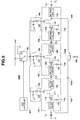
- FIG. 4 The basic configuration of a first embodiment of the present invention is shown in FIG. 4.
- a variable gain amplifier 100 comprises a high frequency amplifier 101 and a high frequency switch circuit 102 for controlling the switching on and off of the signal bypass path for this high frequency amplifier 101.
- the high frequency amplifier 101 taking, for example, FETs as active elements is connected across an input terminal Ti and an output terminal To.
- high frequency switch circuit 102 comprising, for example, FETs is then connected at the middle of a through line 103 connected across the input and output of the high frequency amplifier 101.
- a change-over switch 105 comprising a feed switch that is comprised of, for example, a plurality of FETs is connected across a line from which a power supply voltage Vdd is obtained and a power supply line for the high frequency amplifier 101.
- the side of an input terminal a of this change-over switch 105 is connected to the line from which the power supply voltage Vdd is obtained and the side of an input terminal g of the change-over switch 105 is connected to earth.
- the output terminal of the change-over switch 105 is connected to a change-over control terminal of the high frequency switch circuit 102.
- the change-over switch 105 operates in response to the aforementioned transmission power control information or received signal level and is controlled by a feed controller 301.
- the power supply voltage Vdd passing through the change-over switch 105 is supplied to the high frequency switch circuit 102 as a control signal and the high frequency switch circuit 102 goes off.
- the connection across one input terminal Ti and the output terminal To that passes via the through line 103 is therefore opened.
- the level of the high frequency signal output occurring at the output terminal To becomes higher than the level of the inputted high frequency signal occurring at the input terminal Ti by a gain G101 of the high frequency amplifier 101.
- the level of the high frequency output occurring at the output terminal To is lower than the level in one high frequency signal input occurring at the input terminal Ti by a loss Ls that is the sum of the insertion loss of the high frequency switch circuit 102 and the mismatching loss occurring at the input terminal Ti.
- the gain control width of the variable gain amplifier 100 therefore becomes G101 +
- control is exerted so that the high frequency switch circuit 102 turns the signal bypass path on and off in response to the changing over to the change-over switch 105 for feed control use for the high frequency amplifier 101. Therefore, when functioning of the high frequency amplifier 101 is halted, the feed to the high frequency amplifier 101 is halted. Wasteful power consumption is therefore avoided and gain control range can be dramatically stabilized.
- the high frequency switch circuit 102 of this first embodiment can have a simple configuration of a single FET or a plurality of FETs connected in series. The scale and cost can therefore be substantially received from that of the high frequency change-over switch circuits 53 and 54 of that previously put forward shown in FIG. 3.
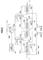
- FIG. 5 A specific configuration of this first embodiment of the present invention is shown in FIG. 5.
- portions corresponding to portions of FIG. 4 are given the same numerals.
- a variable gain amplifier 100A comprises three stages of unit amplifiers 110, 120 and 130 and an FET 102Q taken as a high frequency switch circuit for controlling the putting on and off of a signal bypass path for the unit amplifiers 110 to 130.
- Capacitors Ci, Ca, Cb and Co and unit amplifiers 110, 120 and 130 are connected alternately on after another.
- Each of the unit amplifiers 110, 120 and 130 include FETs 111, 121 and 131, respectively, with the sources of each of these FETs being connected to earth and each unit amplifier being of the same configuration.
- a high frequency signal from the input terminal Ti is supplied to the gate of FET 111 of the first unit amplifier 110 via the input side matching circuit 112 and capacitor Ci and a prescribed gate bias voltage Vgg is supplied via a resistor 113.
- the drain of FET 111 is connected to matching circuit terminal and change-over switch 105 via a high frequency choke coil 117 of a drain bias supply circuit 116.
- the side of the input terminal a of the change-over switch 105 is connected to the line for the power supply voltage Vdd and the side of the input terminal g is connected to ground. Change-over is then controlled by the feed controller 301 in response to transmission power control information or the level of the received signal.
- a high frequency output of the unit amplifier 110 that is taken via the matching circuit 115 of the output side is supplied to a unit amplifier 120 of the following stage via matching capacitor Ca.
- a high frequency signal from the unit amplifier 110 is supplied to the gate of FET 121 of the unit amplifier 120 of the following stage via input side matching circuit 122 and matching capacitor Ca, with a prescribed gate bias voltage Vgg being supplied via resistor 123.
- the drain of FET 121 is connected to a matching circuit 125 and connected to the change-over switch 105 via a high frequency choke coil 127 of a drain bias supply circuit 126.
- a high frequency output of the unit amplifier 120 taken via matching circuit 125 of the output side is supplied to a unit amplifier 130 of the final stage via a junction capacitor Cb.
- a high frequency signal from the unit amplifier 120 is supplied to the gate of FET 131 of the final unit amplifier i30 via an input side matching circuit 132 and junction capacitor Cb, with a prescribed gate bias voltage Vgg being supplied via a terminal 133.
- the drain of FET 131 is connected to a matching circuit 135 and connected to the change-over switch 105 via a high frequency choke coil 137 of a drain bias supply circuit 136.
- a high frequency output of the unit amplifier 130 from the matching circuit 135 of the output side is then taken at the output terminal To via the capacitor Co.
- a depletion type FET 102Q is used as the high frequency switch circuit 102 of this first embodiment.
- the drain of this FET 102Q is connected to the input terminal Ti via a d.c. blocking capacitor 103c and the source of this FET 102Q is connected to the drain of the FET 131 of the unit amplifier 130 of the following stage.
- the gate of the FET 102Q is connected to ground via resistor 106.
- the matching circuits 112 and 115 etc. are given appropriate publicly known configurations.
- Resistors and capacitors (not shown in the drawings) connected in series are also connected at the drain bias supply circuit 116 so as to be in parallel with the high frequency choke coil 117 in order to prevent oscillations.
- resistors 113, 123 and 133 are provided with the purpose of providing isolation, sufficiently large inductors can also be used. Further, the high frequency choke coils 117, 127 and 137 can be replaced with a distributed constant line.
- drain bias voltages Vdd are supplied via the drain bias supply circuits 116, 126 and 136 under the control of the feed controller 301 and the unit amplifier 110, 120 and 130 enter an operating state.
- the drain bias voltage Vdd is supplied to the source of the FET 102Q having its gate connected to earth and a voltage [-Vdd] is applied across the gate and source of FET 102Q.
- the pinch off voltage Vpf of this FET 102Q is given by: Vpf > -Vdd and with the change-over switch 105 in the connection state shown in the drawings, the drain/source junction of the FET 102Q is "off" and the connection across the input terminal Ti and the output terminal To going via the through lines 103 and 104 becomes open.
- the level of the high frequency signal of the output occuring at terminal To is higher than the level of the high frequency signal input occurring at terminal Ti by the total gain of the unit amplifiers 110, 120 and 130 of G110 + G120 + G130.
- the source of FET 102Q is connected to ground via the change-over switch 105 and the high frequency choke coil 137 and a voltage of [0]V is applied across the gate and source of the FET 102Q.
- the drain/source junction of the FET 102Q therefore goes "on” and the input terminal Ti and output terminal To are connected via the through lines 103 and 104.
- the gain control width of the variable gain amplifier 100A becomes G110 + G120 + G130 +
- the FET 102Q controls the turning on and off of the signal bypassing in response to the changing over to the change-over switch 105 for control use with respect to the unit amplifiers 110 to 130. Therefore, when the functioning of the unit amplifiers 110 to 130 is halted, the feed to these unit amplifiers 110 to 130 is halted. Wasteful consumption of power is therefore avoided and gain control range can be dramatically stabilized.
- the high frequency switch circuit 102 of this embodiment can have a simple configuration of a single FET or a plurality of FETs connected in series. The scale and cost can therefore be substantially reduced from that of the high frequency change-over switch circuits 53 and 54 of that previously put forward shown in FIG. 3.
- the FET 102Q taken as the bypass switch can be automatically put on and off so as to control changing over of the change-over switch 105 taken as the feed switch circuit, the complex change-over timing control of the switch of the example of FIG. 2 is no longer necessary.
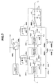
- FIG. 6 and FIG. 7 of a second embodiment of the high frequency variable gain amplifier device of the present invention applied to a power amplifier of the aforementioned transmission circuit.
- FIG. 6 shows a configuration of the second embodiment of the present invention.
- portions corresponding to those of FIG. 5 are given the same numerals or the same numerals for the last two digits.
- a variable gain amplifier 4500 includes unit amplifiers 4510 and 4520 that provide two stages and two FETs 4502a and 4502b taken as high frequency switch circuits for controlling the turning on and off of signal bypassing to the unit amplifiers 4510 and 4520.
- the unit amplifiers 4510 and 4520 include FETs 4511 and 4521, the sources of both of which are connected to earth and are of the same construction.
- the unit amplifiers 4510 and 4520 are connected alternately with capacitors Ci, Cc and Co one after another so as to be inserted across input terminal Ti and output terminal To.
- a high frequency signal from the input terminal Ti is supplied to the gate of FET 4511 of the first unit amplifier 4510 via an input side matching circuit 4512 and capacitor Ci and a prescribed gate bias voltage Vgg is supplied via a resistor 4513.
- the drain of FET 4511 is connected to matching circuit 4515 and is connected to change-over switch 4505 via a high frequenzy choke coil 4517 of a drain bias supply circuit 4516.
- the side of an input terminal a of this change-over switch 4505 is connected to one power supply voltage line Vdd and the side of the input terminal g is connected to earth. Change-over control is then carried out by the feed controller 301 in response to the transmission power control information described previously.
- a high frequency output of the unit amplifier 4510 taken via the matching circuit 4515 on the side of the output is supplied to the following stage unit amplifier 4520 via a junction capacitor Cc.
- a high frequency signal from the unit amplifier 4510 is supplied to the gate of FET 4521 of the unit amplifier 4520 of the following stage via a matching circuit 4522 and capacitor Cc of the input side, with a prescribed gate bias voltage Vgg being supplied via a resistor 4523.
- the drain of FET 4521 is connected to a matching circuit 4525 and is connected to change-over switch 4505 via a high frequency choke coil 4527 of a drain bias supply circuit 4526.
- a high frequency output of the unit amplifier 4520 taken via the matching circuit 4525 of the output side is taken from the output terminal To via the capacitor Co.
- FET 4502a The drain of FET 4502a is then connected to the input terminal Ti via a d.c. blocking capacitor 4503c and the source of FET 4502b is connected to the drain of FET 4521 of the unit amplifier 4520.
- the gates of FET 4502a and 4502b are connected to ground via resistor 4506a and 4506b.
- the matching circuit 4525 for the output side of the unit amplifier 4520 of the final stage depending on the operating frequency and use etc., an example of which is shown in FIG. 7.
- FIG. 7 it is possible to provide a point of connection with the source of the FET 4502b at the matching circuit 4525 when the potential is equal to the drain potential.
- FIG. 7 is exactly the same as FIG. 6 and the description of the remaining portions is therefore omitted.
- the change-over switch 4505 When the transmission output is made high based on the aforementioned transmission power control information, the change-over switch 4505 is put to the connection state shown in the drawings under the control of the feed controller 301, the drain bias voltage Vdd is supplied via the drain bias supply circuits 4516 and 4526 and both of the unit amplifiers 4510 and 4520 are put into operating states.
- the drain bias voltage Vdd of the unit amplifier 4520 is supplied to the source of FET 4502b, the gate of which is connected to earth. A voltage [-Vdd] is then applied across the gate/emitter of the FET 4502b.
- the pinch off voltage Vpf of this FET 4502b is given by: Vpf > -Vdd and with the change-over switch 4505 connected in the state shown in the drawings the drain source junction of the FET 4502b goes “off”, the drain source function of the FET 4502a connected in series with this also goes “off”, and the connection that goes across the input terminal Ti and the output terminal To via the d.c. blocking capacitor 4503c and the through line 4503 is opened.
- the level of the high frequency signal output occurring at the terminal To is higher than the level of the high frequency signal input occurring at the input terminal Ti by just the gain G4520 + G4520(dB) of both the unit amplifiers 4510 and 4520.
- the source of the FET 4502b is connected to earth via the change-over switch 4505 and the high frequency choke coil 4527.
- the drain/source junction of the FET 4502b is then made to go "on” by applying a voltage of [0]V across the gate and source of this FET 4502b.
- the drain/source junction of the FET 4502b also goes on as a result of also applying a voltage of [0]V across the gate and drain of FET 4502a and a connection is made across the input terminal Ti and the output terminal To via the through lines 4503 and 4504.
- the gain control width of the variable gain amplifier 4500 becomes G4510 + F4520 +
- a total gain of 25 dB is obtained in the case of a two stage unit amplifier at a frequency band of 2 GHz.
- the loss for the signal path going via the two switch FETs of an "on" state is about 3 dB including mismatching loss at the input side.
- FET 4502a and FET 4502b control the turning on and off of the signal bypass in response to the change-over of the change-over switch 4505 for feed control with respect to the unit amplifiers 4510 and 4520. Therefore, when the functioning of the unit amplifiers 4510 and 4520 is halted, feeding to these unit amplifiers 4510 and 4520 is halted. Unnecessary power consumption is therefore avoided and a much more stable gain control width is obtained.
- the switch of this embodiment can have a simple configuration of the two FETs 4502a and 4502b connected in series.
- the scale and cost can therefore be substantially reduced from that of the high frequency change-over switch circuits 53 and 54 of that previously put forward shown in FIG. 3.
- the high frequency switch of this embodiment is therefore two FETs 4502a and 4502b connected in series and the isolation of this switch when in an "off" state can therefore be made large.
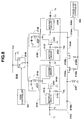
- FIG. 8 A description will be given with reference to FIG. 8 of a third embodiment of the high frequency variable gain amplifier device of the present invention applied to an initial stage of an amplifier of a receiving device.
- FIG. 8 shows a configuration of the third embodiment of the present invention.
- portions corresponding to those of FIG. 5 are given the same numerals or the last two digits are made to be the same.
- a variable gain amplifier 2100 includes two stages of unit amplifiers 2110 and 2120, and two FETs 2102a and 2102b taken as the high frequency bias switch for controlling the turning on and off of a through line 2103 as a signal bypass path with respect to these unit amplifiers 2110 and 2120.
- the unit amplifiers 2110 and 2120 include FETs 2111 and 2121, the sources of both of which are connected to earth and are of the same construction.
- the unit amplifiers 2110 and 2120 are connected alternately with capacitors Ci, Cc and Co one after another so as to be inserted across input terminal Ti and output terminal To.
- a high frequency signal from the input terminal Ti is supplied to the gate of FET 2111 of the first unit amplifier 2110 via an input side matching circuit 2112 and capacitor Ci and a prescribed gate bias voltage Vgg is supplied via a resistor 2113.
- the drain of FET 2111 is connected to matching circuit 2115 and is connected to change-over switch 2105 via a high frequency choke coil 2117 of a drain bias supply circuit 2116.
- the side of an input terminal a of this change-over switch 2105 is connected to the power supply voltage line Vdd and the side of the input terminal g is connected to earth.
- Change-over control is then carried out by the feed controller 301 in response to the transmission power control information describes previously.
- a high frequency output of the unit amplifier 2110 taken via the matching circuit 2115 on the side of the output is supplied to the following stage unit amplifier 2120 via a junction capacitor Cc.
- a high frequency signal from the unit amplifier 2110 is supplied to the gate of FET 2121 of the unit amplifier 2120 of the following stage via a matching circuit 2122 and capacitor Cc of the input side, with a prescribed gate bias voltage Vgg being supplied via a resistor 2123.
- the drain of FET 2121 is connected to a matching circuit 2125 and is connected to chance-over switch 2105 via a high frequency choke coil 2127 of a drain bias supply circuit 2126.
- a high frequency output of the unit amplifier 2120 taken via the matching circuit 2125 of the output side is taken from the output terminal To via the capacitor Co.
- the source of FET 2102a is connected to the input terminal Ti via a d.c. blocking capacitor 2103c and connected to ground via a high frequency choke coil 2107.
- the drain of the remaining FET 2102b is then connected to the drain of the final stage unit amplifier 2120 via a d.c. blocking capacitor 2104c.
- a prescribed control signal S302 from a change-over controller 302 is supplied to the gates of FET 2102a and FED 2102b that are in parallel via resistors 2106a and 2106b in response to the aforementioned received level.
- connection end of the source of FET 2102a is by no means limited to portions supplied with the drain bias voltage Vdd such as, for example, the unit amplifier 2120 and can be selected within an appropriate scope.
- the FETs 2102a and 2102b are by no means limited to the depression type of the case described in FIG. 6 and operation is also possible with an enhancement type.
- the change-over switch 2105 goes into the connection state shown in the drawings under the control of the feed controller 301 and the d.c. level of the control signal S302 from the change-over controller 302 becomes lower [Vgg] than the pinch off voltage Vpf of the FET 2102a and FET 2102b.
- Both of the unit amplifiers 2110 and 2120 are then supplied with the drain bias voltage Vdd via the change-over switch 2105 and the drain bias supply circuits 2115 and 2126 and therefore enter operating states.
- the drain/source junction of the FET 2102a then goes "off", the drain/source function of the FET 2102b connected in parallel with FET 2102a also goes off, and the connection across the input terminal Ti and the output terminal To via the d.c. blocking capacitor 2103c, through lines 2103 and 2104 and the the d.c. blocking capacitor 2104c is then made to be open.
- the level of the high frequency signal output occuring at the output terminal To is higher than the level of the high frequency signal input occurring at the input terminal Ti by the gains G2110 + G2120 of both of the unit amplifiers 2110 and 2120.
- the change-over switch 2105 is changed over to the state that is the opposite of the state shown in the drawings and the d.c. level of the control signal S302 from the change-over controller 302 is changed over to the ground potential.
- the supplying of the drain bias voltages is then shut off and both of the unit amplifiers 2110 and 2120 cease operation.
- the gate and sources become of the same potential to allow the "on" state between the drain and the source of the FET 2102a.
- the gate and source of the FET 2102b connected in series with this FET become of the same potential to allow also the "on” state between the drain and the source of the FET 2102b.
- the input terminal Ti and the output terminal To are therefore connected via the d.c. blocking capacitor 2103c, through lines 2103 and 2104 and the d.c. blocking capacitor 2104c.
- the gain control range of the variable gain amplifier 2100 due to the switching of the change-over switch 205 becomes G2110 + G2120 +
- FET 2102a and FET 2102b control the turning on and off of the signal bypass in response to change-over of the change-over switch 2105 for feed control use with respect to the unit amplifiers 2110 and 2120 under the control of the feed controller 301 and the change-over controller 302.
- the functioning of the unit amplifiers 2110 and 2120 is halted, feeding to the unit amplifiers 2110 and 2120 is halted so that wasteful consumption of power is avoided and a markedly more stable gain control range is obtained.
- the high frequency switch of this third embodiment has a simple configuration of the two FETs 2102a and 2102b connected in series.
- the scale and cost can therefore be substantially reduced from that of the high frequency change-over switch circuits 53 and 54 of that previously put forward shown in FIG. 3.
- the high frequency switch of this third embodiment is therefore two FETs 2102a and 2102b connected in series and the isolation when in an "off" state can therefore be made sufficient.
- FETs are used as both the active elements of the amplifiers and are used in the high frequency switch but the present invention is by no means limited in this respect and bipolar transistors can also be used.
- a stable gain control range can be obtained for each stage using a simple configuration; power consumption can be reduced and the scale of circuitry used in gain control can be reduced.
- Control of the timing of the changing over of the feed switch and the bias switch is therefore no longer necessary and ccncrol is easier as a result.
Landscapes
- Engineering & Computer Science (AREA)
- Power Engineering (AREA)
- Computer Networks & Wireless Communication (AREA)
- Signal Processing (AREA)
- Amplifiers (AREA)
- Control Of Amplification And Gain Control (AREA)
- Transceivers (AREA)
Applications Claiming Priority (3)
| Application Number | Priority Date | Filing Date | Title |
|---|---|---|---|
| JP344664/96 | 1996-12-09 | ||
| JP8344664A JPH10173453A (ja) | 1996-12-09 | 1996-12-09 | 高周波可変利得増幅装置および無線通信装置 |
| JP34466496 | 1996-12-09 |
Publications (2)
| Publication Number | Publication Date |
|---|---|
| EP0847135A2 true EP0847135A2 (fr) | 1998-06-10 |
| EP0847135A3 EP0847135A3 (fr) | 1999-12-22 |
Family
ID=18371031
Family Applications (1)
| Application Number | Title | Priority Date | Filing Date |
|---|---|---|---|
| EP97309816A Withdrawn EP0847135A3 (fr) | 1996-12-09 | 1997-12-04 | Dispositif amplificateur haute fréquence à gain variable |
Country Status (5)
| Country | Link |
|---|---|
| US (1) | US6118989A (fr) |
| EP (1) | EP0847135A3 (fr) |
| JP (1) | JPH10173453A (fr) |
| KR (1) | KR100479974B1 (fr) |
| CN (1) | CN1139182C (fr) |
Cited By (16)
| Publication number | Priority date | Publication date | Assignee | Title |
|---|---|---|---|---|
| WO2000018006A1 (fr) * | 1998-09-21 | 2000-03-30 | Koninklijke Philips Electronics N.V. | Amplificateur |
| EP0998032A3 (fr) * | 1998-10-26 | 2001-04-11 | SPAUN-electronic GmbH & Co. KG | Dispositif amplificateur pour signaux radiofréquences |
| GB2356503A (en) * | 1999-09-07 | 2001-05-23 | Agilent Technologies Inc | A high frequency amplifier with a by-pass switch for use in a receiver |
| WO2002015397A3 (fr) * | 2000-08-16 | 2003-09-25 | Maxim Integrated Products | Amplificateur a grande linearite et adaptation d'impedance comportant un mode de derivation a faible perte |
| WO2003005566A3 (fr) * | 2001-07-06 | 2004-01-22 | Infineon Technologies Ag | Circuit d'amplification à faible bruit |
| EP1184974A3 (fr) * | 2000-08-07 | 2004-03-03 | Sony Corporation | Unité d'antenne et circuit de réception |
| US7064604B2 (en) | 2001-07-12 | 2006-06-20 | Kathrein-Werke Kg | Amplifier switch |
| EP1162731A3 (fr) * | 2000-06-08 | 2006-10-25 | Sumitomo Electric Industries, Ltd. | Circuit amplificateur aux microondes, dispositif amplificateur aux microondes, et circuit de compensation |
| US7317903B2 (en) | 2003-09-30 | 2008-01-08 | Sharp Kabushiki Kaisha | Wireless communication circuit, wireless communication apparatus, and wireless communication system |
| EP1839389A4 (fr) * | 2005-01-10 | 2009-12-09 | Texas Instruments Inc | Circuit amplificateur differentiel et procede permettant de reduire les compensations d'origine thermique causees par de grands signaux differentiels |
| EP1802009A3 (fr) * | 2005-12-23 | 2012-04-25 | Samsung Electronics Co., Ltd. | Récepteur pour la réception de la radiodiffusion numérique ainsi que méthode pour optimiser la consommation énergétique dans un récepteur pour la réception de la radiodiffusion numérique |
| CN101207399B (zh) * | 2006-12-06 | 2014-06-04 | 美国博通公司 | 在发射器中控制电路的方法和系统 |
| EP3139500A1 (fr) * | 2015-09-01 | 2017-03-08 | Onkyo Corporation | Dispositif de reproduction de musique |
| CN113411053A (zh) * | 2020-03-17 | 2021-09-17 | 株式会社东芝 | 半导体装置 |
| WO2022132304A1 (fr) * | 2020-12-18 | 2022-06-23 | Northrop Grumman Systems Corporation | Sommateur rf à large bande commutable de manière sélective |
| WO2024172968A1 (fr) * | 2023-02-14 | 2024-08-22 | Qualcomm Incorporated | Commutateur de tête pour une structure de transistor empilée |
Families Citing this family (62)
| Publication number | Priority date | Publication date | Assignee | Title |
|---|---|---|---|---|
| US6127886A (en) * | 1997-10-30 | 2000-10-03 | The Whitaker Corporation | Switched amplifying device |
| JP3587346B2 (ja) * | 1998-08-07 | 2004-11-10 | 松下電器産業株式会社 | 無線通信装置および無線通信装置における送信電力制御方法 |
| KR100556470B1 (ko) * | 1998-12-31 | 2006-05-25 | 엘지전자 주식회사 | 이동통신 단말기용 전력증폭기의 구동 제어회로 |
| EP1022848B1 (fr) * | 1999-01-19 | 2010-05-05 | Panasonic Corporation | Amplificateur et dispositif de radiocommunication utilisant un tel amplificateur |
| EP1032120A3 (fr) * | 1999-02-26 | 2003-07-30 | Matsushita Electric Industrial Co., Ltd. | Amplificateur de puissance, méthode de commande de la puissance d'un amplificateur de puissance et équipement de communication |
| TW512595B (en) * | 1999-03-04 | 2002-12-01 | Benq Corp | Signal transmission circuit for wireless cellular phone |
| US6463267B1 (en) | 1999-04-21 | 2002-10-08 | Hitachi, Ltd. | High frequency power amplifying apparatus having amplifying stages with gain control signals of lower amplitudes applied to earlier preceding stages |
| US6271722B1 (en) * | 1999-09-28 | 2001-08-07 | Qualcomm Inc. | Partial or complete amplifier bypass |
| US6473600B1 (en) | 1999-12-13 | 2002-10-29 | Koninklijke Philips Electronics N.V. | Mobile phone with increased transmitter efficiency employing two transmit antennas |
| US6625238B2 (en) * | 2000-03-29 | 2003-09-23 | Sony Corporation | Low power and high linearity receivers with reactively biased front ends |
| US6668028B1 (en) * | 2000-03-29 | 2003-12-23 | Sony Corporation | Low-power CDMA receiver |
| US6782062B1 (en) * | 2000-03-29 | 2004-08-24 | Sony Corporation | Low power and high linearity receivers with reactively biased front ends |
| FI114261B (fi) * | 2000-09-12 | 2004-09-15 | Nokia Corp | Lähetin ja langaton viestintälaite |
| US6734724B1 (en) | 2000-10-06 | 2004-05-11 | Tropian, Inc. | Power control and modulation of switched-mode power amplifiers with one or more stages |
| US6586993B2 (en) * | 2000-11-08 | 2003-07-01 | Research In Motion Limited | Impedance matching low noise amplifier having a bypass switch |
| DE10056877B4 (de) * | 2000-11-16 | 2006-08-10 | Robert Bosch Gmbh | Empfängerempfindlichkeit |
| KR100487813B1 (ko) * | 2001-01-19 | 2005-05-10 | 인티그런트 테크놀로지즈(주) | 상보 소자를 이용한 싱글엔드형 차동 회로 |
| JP4220694B2 (ja) * | 2001-03-27 | 2009-02-04 | パナソニック株式会社 | 高周波可変利得増幅装置 |
| EP1386237A4 (fr) * | 2001-04-20 | 2007-10-17 | American Express Travel Relate | Systeme et procede de gestion et d'optimalisation de contrats de transporteurs aeriens |
| US7856359B2 (en) * | 2001-07-02 | 2010-12-21 | American Express Travel Related Services Company, Inc. | System and method for airline purchasing program management |
| US6680652B2 (en) | 2001-08-06 | 2004-01-20 | Rf Micro Devices, Inc. | Load switching for transmissions with different peak-to-average power ratios |
| US20050288974A1 (en) * | 2001-08-23 | 2005-12-29 | American Express Travel Related Services Company, Inc. | Travel service broker system and method |
| US7539620B2 (en) * | 2002-07-02 | 2009-05-26 | American Express Travel Related Services Company, Inc. | System and method for facilitating transactions among consumers and providers of travel services |
| US20040260581A1 (en) * | 2001-08-23 | 2004-12-23 | American Express Travel Related Services Company, Inc. | Travel market broker system |
| US7499864B2 (en) * | 2002-01-25 | 2009-03-03 | American Express Travel Related Services Company, Inc. | Integrated travel industry system |
| US7061993B2 (en) * | 2001-08-29 | 2006-06-13 | Sony Corporation | CDMA receiver architecture for lower bypass switch point |
| US6819941B2 (en) | 2001-10-11 | 2004-11-16 | Rf Micro Devices, Inc. | Single output stage power amplification for multimode applications |
| EP1309083A1 (fr) * | 2001-11-06 | 2003-05-07 | Siemens Aktiengesellschaft | Méthode de commutation de gain d'un amplificateur et amplificateur à faible bruit de fond comportant une commutation de gain |
| US6680647B2 (en) * | 2001-12-13 | 2004-01-20 | Agilent Technologies, Inc. | Low noise amplifier circuit with phase matched switch topology |
| US6687491B2 (en) * | 2002-01-18 | 2004-02-03 | Sony Corporation | Direct conversion of low power high linearity receiver |
| US7805323B2 (en) | 2002-01-25 | 2010-09-28 | American Express Travel Related Services Company, Inc. | System and method for processing trip requests |
| US7235050B2 (en) * | 2002-04-11 | 2007-06-26 | Alfred E. Mann Foundation For Scientific Research | Implantable device for processing neurological signals |
| JP4050096B2 (ja) * | 2002-05-31 | 2008-02-20 | 松下電器産業株式会社 | 高周波スイッチ回路および移動体通信端末装置 |
| US6806767B2 (en) * | 2002-07-09 | 2004-10-19 | Anadigics, Inc. | Power amplifier with load switching circuit |
| JP4121844B2 (ja) | 2002-12-12 | 2008-07-23 | 新日本無線株式会社 | 利得可変型増幅器 |
| US20050104766A1 (en) * | 2003-11-14 | 2005-05-19 | Brian Bandhauer | Radar detection zone pattern shaping |
| US7161427B2 (en) * | 2003-12-22 | 2007-01-09 | Silicon Laboratories Inc. | Input structure for a power amplifier and associated methods |
| US7212070B2 (en) * | 2003-12-22 | 2007-05-01 | Silicon Laboratories Inc. | Circuit and method of reducing noise in an RF power amplifier |
| US7113045B2 (en) * | 2003-12-22 | 2006-09-26 | Silicon Laboratories Inc. | Power amplifier input structure having a differential output |
| US7064605B2 (en) * | 2003-12-22 | 2006-06-20 | Silicon Laboratories Inc. | Circuit and method of establishing DC bias levels in an RF power amplifier |
| JP4137814B2 (ja) * | 2004-02-19 | 2008-08-20 | ソニー・エリクソン・モバイルコミュニケーションズ株式会社 | スイッチ装置、スイッチ付電力増幅装置及び携帯通信端末装置 |
| JP2006005839A (ja) * | 2004-06-21 | 2006-01-05 | Samsung Electronics Co Ltd | 増幅器 |
| JP2006135518A (ja) * | 2004-11-04 | 2006-05-25 | Alps Electric Co Ltd | 高周波増幅器 |
| KR100644273B1 (ko) * | 2004-12-21 | 2006-11-10 | 한국전자통신연구원 | 광대역 가변 입력 매칭 저잡음 증폭기 |
| JP2007081535A (ja) * | 2005-09-12 | 2007-03-29 | Toshiba Corp | 可変利得増幅器 |
| JP4725962B2 (ja) * | 2005-12-16 | 2011-07-13 | 株式会社ソニー・コンピュータエンタテインメント | 通信端末装置および送信電力制御方法 |
| KR101125948B1 (ko) * | 2005-12-28 | 2012-03-21 | 엘지전자 주식회사 | 다단계의 가변이득을 갖는 저잡음 증폭장치 및 그 방법 |
| TWI318498B (en) * | 2006-05-08 | 2009-12-11 | Novatek Microelectronics Corp | Variable gain amplifying circuit and method of changing the gain amplifying path |
| US8095082B2 (en) * | 2007-10-10 | 2012-01-10 | Qualcomm, Incorporated | Dual band radio frequency transmitter |
| JP4896903B2 (ja) * | 2008-02-09 | 2012-03-14 | 新日本無線株式会社 | 増幅器 |
| US8536950B2 (en) * | 2009-08-03 | 2013-09-17 | Qualcomm Incorporated | Multi-stage impedance matching |
| US8102205B2 (en) | 2009-08-04 | 2012-01-24 | Qualcomm, Incorporated | Amplifier module with multiple operating modes |
| JP5596451B2 (ja) * | 2010-07-16 | 2014-09-24 | 新日本無線株式会社 | 利得可変型増幅器 |
| RU2561029C1 (ru) * | 2011-06-27 | 2015-08-20 | Хьюлетт-Паккард Дивелопмент Компани, Л.П. | Датчик уровня чернил и относящиеся к нему способы |
| WO2013157039A1 (fr) * | 2012-04-18 | 2013-10-24 | 三菱電機株式会社 | Amplificateur de puissance électrique à commutation de trajet |
| JPWO2013157039A1 (ja) * | 2012-04-18 | 2015-12-21 | 三菱電機株式会社 | 経路切替電力増幅器 |
| CN104158505A (zh) * | 2013-05-14 | 2014-11-19 | 中兴通讯股份有限公司 | 一种射频功放电路、控制方法及终端 |
| CN104167991B (zh) * | 2013-05-17 | 2017-10-24 | 日月光半导体制造股份有限公司 | 可变增益低噪声放大电路及其可变增益方法与接收机 |
| JP6336775B2 (ja) * | 2014-02-19 | 2018-06-06 | 新日本無線株式会社 | 利得可変型増幅器 |
| WO2016125424A1 (fr) * | 2015-02-06 | 2016-08-11 | 日本電気株式会社 | Circuit d'alimentation de source de courant, amplificateur, dispositif de communication, station de base, et procédé d'alimentation de source de courant |
| TWI617131B (zh) * | 2016-12-30 | 2018-03-01 | 立積電子股份有限公司 | 放大電路 |
| CN116979911B (zh) * | 2023-09-20 | 2023-12-15 | 中科海高(成都)电子技术有限公司 | 一种放大器结构、控制方法、芯片及电子设备 |
Family Cites Families (12)
| Publication number | Priority date | Publication date | Assignee | Title |
|---|---|---|---|---|
| FI81931C (fi) * | 1989-05-12 | 1990-12-10 | Nokia Mobira Oy | Foerfarande foer alstring av laoga effektnivaoer i saendaren av en radiotelefon. |
| EP0462782B1 (fr) * | 1990-06-16 | 1995-03-01 | Nec Corporation | Récepteur pour un système de communication radio cellulaire mobile |
| US5060294A (en) * | 1990-07-05 | 1991-10-22 | Motorola, Inc. | Dual mode power amplifier for radiotelephone |
| US5216378A (en) * | 1992-03-02 | 1993-06-01 | Motorola, Inc. | Switch adaptable radio frequency amplifier |
| US5432473A (en) * | 1993-07-14 | 1995-07-11 | Nokia Mobile Phones, Limited | Dual mode amplifier with bias control |
| US5399927A (en) * | 1993-12-03 | 1995-03-21 | Itt Corporation | Solid state bypass circuit for RF and microwave active circuits |
| JP3432262B2 (ja) * | 1994-01-19 | 2003-08-04 | 株式会社東芝 | 無線電話装置 |
| US5661434A (en) * | 1995-05-12 | 1997-08-26 | Fujitsu Compound Semiconductor, Inc. | High efficiency multiple power level amplifier circuit |
| JPH09135127A (ja) * | 1995-11-07 | 1997-05-20 | Nec Corp | 電力増幅器 |
| JPH09148852A (ja) * | 1995-11-24 | 1997-06-06 | Matsushita Electric Ind Co Ltd | 送信出力可変装置 |
| JPH09162773A (ja) * | 1995-12-07 | 1997-06-20 | Nec Corp | 消費電流低減機能付無線送受信装置 |
| JP2877081B2 (ja) * | 1996-06-26 | 1999-03-31 | 日本電気株式会社 | 移動体通信装置 |
-
1996
- 1996-12-09 JP JP8344664A patent/JPH10173453A/ja active Pending
-
1997
- 1997-11-19 US US08/974,623 patent/US6118989A/en not_active Expired - Fee Related
- 1997-11-25 KR KR1019970062840A patent/KR100479974B1/ko not_active Expired - Fee Related
- 1997-12-04 EP EP97309816A patent/EP0847135A3/fr not_active Withdrawn
- 1997-12-09 CN CNB97129738XA patent/CN1139182C/zh not_active Expired - Fee Related
Cited By (21)
| Publication number | Priority date | Publication date | Assignee | Title |
|---|---|---|---|---|
| WO2000018006A1 (fr) * | 1998-09-21 | 2000-03-30 | Koninklijke Philips Electronics N.V. | Amplificateur |
| EP0998032A3 (fr) * | 1998-10-26 | 2001-04-11 | SPAUN-electronic GmbH & Co. KG | Dispositif amplificateur pour signaux radiofréquences |
| GB2356503B (en) * | 1999-09-07 | 2004-02-25 | Agilent Technologies Inc | Amplifier circuit with a switch bypass |
| GB2356503A (en) * | 1999-09-07 | 2001-05-23 | Agilent Technologies Inc | A high frequency amplifier with a by-pass switch for use in a receiver |
| EP1162731A3 (fr) * | 2000-06-08 | 2006-10-25 | Sumitomo Electric Industries, Ltd. | Circuit amplificateur aux microondes, dispositif amplificateur aux microondes, et circuit de compensation |
| US7212796B2 (en) | 2000-08-07 | 2007-05-01 | Sony Corporation | Antenna unit and receiving circuit |
| EP1184974A3 (fr) * | 2000-08-07 | 2004-03-03 | Sony Corporation | Unité d'antenne et circuit de réception |
| WO2002015397A3 (fr) * | 2000-08-16 | 2003-09-25 | Maxim Integrated Products | Amplificateur a grande linearite et adaptation d'impedance comportant un mode de derivation a faible perte |
| US7057457B2 (en) | 2001-07-06 | 2006-06-06 | Infineon Technologies Ag | Low-noise amplifying circuit |
| WO2003005566A3 (fr) * | 2001-07-06 | 2004-01-22 | Infineon Technologies Ag | Circuit d'amplification à faible bruit |
| US7064604B2 (en) | 2001-07-12 | 2006-06-20 | Kathrein-Werke Kg | Amplifier switch |
| US7317903B2 (en) | 2003-09-30 | 2008-01-08 | Sharp Kabushiki Kaisha | Wireless communication circuit, wireless communication apparatus, and wireless communication system |
| EP1839389A4 (fr) * | 2005-01-10 | 2009-12-09 | Texas Instruments Inc | Circuit amplificateur differentiel et procede permettant de reduire les compensations d'origine thermique causees par de grands signaux differentiels |
| EP1802009A3 (fr) * | 2005-12-23 | 2012-04-25 | Samsung Electronics Co., Ltd. | Récepteur pour la réception de la radiodiffusion numérique ainsi que méthode pour optimiser la consommation énergétique dans un récepteur pour la réception de la radiodiffusion numérique |
| CN101207399B (zh) * | 2006-12-06 | 2014-06-04 | 美国博通公司 | 在发射器中控制电路的方法和系统 |
| EP3139500A1 (fr) * | 2015-09-01 | 2017-03-08 | Onkyo Corporation | Dispositif de reproduction de musique |
| US9712919B2 (en) | 2015-09-01 | 2017-07-18 | Onkyo Corporation | Music reproducing device with first and second D/A converters for converting audio signals prior to inversion |
| CN113411053A (zh) * | 2020-03-17 | 2021-09-17 | 株式会社东芝 | 半导体装置 |
| WO2022132304A1 (fr) * | 2020-12-18 | 2022-06-23 | Northrop Grumman Systems Corporation | Sommateur rf à large bande commutable de manière sélective |
| US11616477B2 (en) | 2020-12-18 | 2023-03-28 | Northrop Grumman Systems Corporation | Selectively switchable wideband RF summer |
| WO2024172968A1 (fr) * | 2023-02-14 | 2024-08-22 | Qualcomm Incorporated | Commutateur de tête pour une structure de transistor empilée |
Also Published As
| Publication number | Publication date |
|---|---|
| US6118989A (en) | 2000-09-12 |
| JPH10173453A (ja) | 1998-06-26 |
| EP0847135A3 (fr) | 1999-12-22 |
| CN1139182C (zh) | 2004-02-18 |
| KR100479974B1 (ko) | 2005-07-25 |
| KR19980063611A (ko) | 1998-10-07 |
| CN1193844A (zh) | 1998-09-23 |
Similar Documents
| Publication | Publication Date | Title |
|---|---|---|
| US6118989A (en) | High frequency variable gain amplifier device and wireless communications terminal | |
| KR100844398B1 (ko) | 다중 레벨 전력 증폭기 | |
| US5548246A (en) | Power amplifier including an impedance matching circuit and a switch FET | |
| EP0883250B1 (fr) | Emetteur de communications mobiles avec des amplificateurs sélectivement activés | |
| EP0700169B1 (fr) | Commutateur réception-émission pour appareil de radio-communication | |
| US5758269A (en) | High-efficient configurable power amplifier for use in a portable unit | |
| CA2273151C (fr) | Amplificateur de puissance a etages paralleles efficace | |
| EP0673112B1 (fr) | Amplificateur de puissance et méthode d'amplification | |
| US6972618B2 (en) | High efficiency power amplifier with multiple power modes | |
| EP0482502B1 (fr) | Amplificateur de puissance et appareil radio mobile équipé d'un tel amplificateur | |
| KR20050065887A (ko) | 개선된 전력증폭기 효율을 가진 듀얼 안테나 다이버시티송신기 및 시스템 | |
| US7215192B2 (en) | High efficiency power amplifier | |
| WO2004062095A1 (fr) | Amplificateur de puissance a haut rendement a plusieurs modes de puissance | |
| US7439809B2 (en) | Radio frequency power amplifier | |
| AU4720599A (en) | Systems and methods for management of current consumption and performance in a receiver down converter of a wireless device | |
| EP1154566B1 (fr) | Circuit de polarisation et appareil de communication radio utilisant un tel circuit | |
| EP0622895B1 (fr) | Appareil de communication avec amplificateur de puissance | |
| US5216378A (en) | Switch adaptable radio frequency amplifier | |
| EP1229642A1 (fr) | Amplificateur de puissance pour amplifier des signaux radiofréquences | |
| EP1122883B1 (fr) | Circuit de linéarisation d'un profil de contrôle de puissance d'un amplificateur de puissance BiCMOS | |
| JPH11145748A (ja) | 電力増幅回路 | |
| JPH06350478A (ja) | 通信装置 | |
| EP1317062A2 (fr) | Contrôle de l'alimentation d'amplificateurs en cascade dans un circuit de transmission | |
| JPH09321637A (ja) | 無線送信装置およびその制御方法 | |
| JP2003069440A (ja) | 携帯電話機 |
Legal Events
| Date | Code | Title | Description |
|---|---|---|---|
| PUAI | Public reference made under article 153(3) epc to a published international application that has entered the european phase |
Free format text: ORIGINAL CODE: 0009012 |
|
| AK | Designated contracting states |
Kind code of ref document: A2 Designated state(s): DE FI FR GB SE |
|
| AX | Request for extension of the european patent |
Free format text: AL;LT;LV;MK;RO;SI |
|
| PUAL | Search report despatched |
Free format text: ORIGINAL CODE: 0009013 |
|
| AK | Designated contracting states |
Kind code of ref document: A3 Designated state(s): AT BE CH DE DK ES FI FR GB GR IE IT LI LU MC NL PT SE |
|
| AX | Request for extension of the european patent |
Free format text: AL;LT;LV;MK;RO;SI |
|
| 17P | Request for examination filed |
Effective date: 20000523 |
|
| AKX | Designation fees paid |
Free format text: DE FI FR GB SE |
|
| STAA | Information on the status of an ep patent application or granted ep patent |
Free format text: STATUS: THE APPLICATION HAS BEEN WITHDRAWN |
|
| 18W | Application withdrawn |
Withdrawal date: 20020930 |