EP0854485A2 - Mémoire synchrone à semiconducteurs capable d'améliorer la charge d'une ligne de signal d'horloge - Google Patents
Mémoire synchrone à semiconducteurs capable d'améliorer la charge d'une ligne de signal d'horloge Download PDFInfo
- Publication number
- EP0854485A2 EP0854485A2 EP98100866A EP98100866A EP0854485A2 EP 0854485 A2 EP0854485 A2 EP 0854485A2 EP 98100866 A EP98100866 A EP 98100866A EP 98100866 A EP98100866 A EP 98100866A EP 0854485 A2 EP0854485 A2 EP 0854485A2
- Authority
- EP
- European Patent Office
- Prior art keywords
- clock signal
- internal clock
- level
- signal
- data
- Prior art date
- Legal status (The legal status is an assumption and is not a legal conclusion. Google has not performed a legal analysis and makes no representation as to the accuracy of the status listed.)
- Withdrawn
Links
Images


Classifications
-
- G—PHYSICS
- G11—INFORMATION STORAGE
- G11C—STATIC STORES
- G11C11/00—Digital stores characterised by the use of particular electric or magnetic storage elements; Storage elements therefor
- G11C11/21—Digital stores characterised by the use of particular electric or magnetic storage elements; Storage elements therefor using electric elements
- G11C11/34—Digital stores characterised by the use of particular electric or magnetic storage elements; Storage elements therefor using electric elements using semiconductor devices
- G11C11/40—Digital stores characterised by the use of particular electric or magnetic storage elements; Storage elements therefor using electric elements using semiconductor devices using transistors
- G11C11/41—Digital stores characterised by the use of particular electric or magnetic storage elements; Storage elements therefor using electric elements using semiconductor devices using transistors forming static cells with positive feedback, i.e. cells not needing refreshing or charge regeneration, e.g. bistable multivibrator or Schmitt trigger
- G11C11/413—Auxiliary circuits, e.g. for addressing, decoding, driving, writing, sensing, timing or power reduction
-
- G—PHYSICS
- G11—INFORMATION STORAGE
- G11C—STATIC STORES
- G11C7/00—Arrangements for writing information into, or reading information out from, a digital store
- G11C7/10—Input/output [I/O] data interface arrangements, e.g. I/O data control circuits, I/O data buffers
- G11C7/1051—Data output circuits, e.g. read-out amplifiers, data output buffers, data output registers, data output level conversion circuits
- G11C7/1066—Output synchronization
-
- G—PHYSICS
- G11—INFORMATION STORAGE
- G11C—STATIC STORES
- G11C7/00—Arrangements for writing information into, or reading information out from, a digital store
- G11C7/10—Input/output [I/O] data interface arrangements, e.g. I/O data control circuits, I/O data buffers
- G11C7/1015—Read-write modes for single port memories, i.e. having either a random port or a serial port
- G11C7/1018—Serial bit line access mode, e.g. using bit line address shift registers, bit line address counters, bit line burst counters
-
- G—PHYSICS
- G11—INFORMATION STORAGE
- G11C—STATIC STORES
- G11C7/00—Arrangements for writing information into, or reading information out from, a digital store
- G11C7/10—Input/output [I/O] data interface arrangements, e.g. I/O data control circuits, I/O data buffers
- G11C7/1051—Data output circuits, e.g. read-out amplifiers, data output buffers, data output registers, data output level conversion circuits
-
- G—PHYSICS
- G11—INFORMATION STORAGE
- G11C—STATIC STORES
- G11C7/00—Arrangements for writing information into, or reading information out from, a digital store
- G11C7/10—Input/output [I/O] data interface arrangements, e.g. I/O data control circuits, I/O data buffers
- G11C7/1072—Input/output [I/O] data interface arrangements, e.g. I/O data control circuits, I/O data buffers for memories with random access ports synchronised on clock signal pulse trains, e.g. synchronous memories, self timed memories
Definitions
- the present invention relates to a synchronous semiconductor memory device and, more particularly, it relates to an improvement on a heavily loaded signal line that is adapted to operate at a high frequency.
- DRAM dynamic random access memory
- a synchronous semiconductor memory device latches an external address with a data write/read instruction and executes the operation of reading/writing the data at the external address and then it receives a synchronous clock signal and generates predetermined internal addresses starting from the external address to read/write the data at the internal addresses.
- a synchronous DRAM is a DRAM that operates in synchronization with a clock signal, so that the data with the addresses that are internally and automatically generated following the data at the address latched by a read/write instruction are continuously output at high speed or data are input to the addresses continuously at high speed. This is called a burst operation.
- an internal clock generation circuit generates an internal clock signal having a frequency equal to the frequency of the external clock signal
- a data output circuit outputs the data read out of the memory cell array in synchronization with the internal clock signal.
- the internal clock signal operates at the same frequency as that of the external clock signal, so that the life span of a signal line for the internal clock signal is reduced by deterioration of its reliability due to electro-migration.
- an internal clock generation circuit generates an internal clock signal having a frequency equal to 1/2 of the frequency of the external clock signal in synchronization with the external clock signal
- a data output circuit outputs the data read out of the memory cell array in synchronization with both a rising edge and a falling edge of the internal clock signal.
- a memory cell array is divided into at least first and second blocks.
- a first data output means outputs the data read out of the first block of the memory cell array in synchronization with a rising edge of the internal clock signal
- a second data output means outputs the data read out of the second block of the memory cell array in synchronization with a falling edge of the internal clock signal.
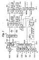
- an input circuit 1 receives an external address signal ADD and outputs an internal address signal IADD.
- An input circuit 2 receives a row address strobe signal RAS and outputs an internal signal IRAS
- an input circuit 3 receives a column address strobe signal CAS and outputs an internal signal ICAS.
- an input circuit 4 receives a write enable signal WE and outputs an internal signal IWE
- an input circuit 5 receives a chip select signal CS and outputs internal signal ICS
- an input circuit 6 receives an external clock signal CLK and outputs an internal clock signal ICLK1. Note that the input circuits 2 through 5 operate at a rising edge of the external clock signal CLK.
- a command decoder 7 receives the internal signals IRAS, ICAS, IWE and ICS and outputs signals READ1 and READ2 in synchronization with the internal clock signal ICLK1.
- a burst counter 8 latches the internal address signal IADD according to the signal READ1 and counts up the latched internal address signal IADD according to the internal clock signal ICLK1 to automatically generate a column address signal YADD.
- a column decoder 9 receives the column address signal YADD and sequentially selects column switch lines YSW1 through YSWn.
- Sense amplifiers S11, S21, ⁇ , S1n, S2n, ... are connected between the column switch lines YS1, ⁇ , YSWn and read buses RBUS1, RBUS2, ⁇ .
- the sense amplifiers S11, S21, . ⁇ output data to the read buses RBUS11, RBUS12, ⁇ .
- cell columns C11, C21, ⁇ , C1n, C2n, ⁇ are connected to the sense amplifiers S11, S21, ⁇ , S1n, S2n, ⁇ by way of digit lines D11, D21, ⁇ , D1n, D2n, ⁇ , respectively.
- each of the cell columns C11, C21, ⁇ , C1n, C2n, ⁇ represents a plurality of cells which are selected by a row decoder (not shown).
- a row decoder not shown
- a cell array is divided into m blocks BK1, BK2, ⁇ , only two of them, or blocks BK1 and BK2 are shown for simplicity.
- the read buses RBUS1, RBUS2, ... are respectively connected to data amplifiers 11-1, 11-2, ... , which are connected by turn to read buses RBUS21, RBUS22, ⁇ .
- the read buses RBUS21, RBUS22, ⁇ are then connected to output circuits 12-1, 12-2, ⁇ , which are connected by turn to output terminals OUT1, OUT2, ⁇ , respectively.
- the data amplifiers 11-1, 11-2, are controlled by an internal clock generation circuit 13-A. More specifically, the internal clock generation circuit 13-A receives the signal READ2 from the command decoder 7 and outputs an internal clock signal ICLK3 that is synchronized with the internal clock signal ICLK1.
- the internal clock generation circuit 13-A is formed by a delay circuit DL that delays the internal clock signal ICLK1 and outputs an internal clock signal ICLK2, inverters I1, I2, I3 that invert and delay the internal clock signal ICLK2, a NAND circuit G1 that receives the internal clock signal ICLK2 and its inverted and delayed signal ICLK2 , and an inverter I4.
- the NAND circuit G1 also receives the signal READ2. Therefore, the internal clock generation circuit 13-A is enabled only when the signal READ2 is high. In other words, the internal clock generation circuit 13-A outputs the internal clock signal ICLK3 that is synchronized with the internal clock signal ICLK1 when the signal READ2 is high.
- an external clock signal CLK is input as indicated in FIG. 2A and, as a result, signals RAS , CAS , WE and CE are input at a rising edge of the external clock signal CLK to show a read command as indicated by FIG. 2B.
- the internal clock signal CLK1 is generated in synchronization with the external clock signal CLK, and also, an external address signal ADD as shown in FIG. 2C becomes an internal address signal IADD as shown in FIG. 2E.
- the command decoder 7 Upon receiving the read command, the command decoder 7 outputs high level signals READ1 and READ2 as shown in FIGS. 2F and 2G in synchronization with the internal clock signal CLK1.
- the signal READ1 is brought to a low level in synchronization with the next rising edge of the internal clock signal CLK1.
- the burst counter 8 Upon receiving the high level signal READ1, the burst counter 8 latches and outputs the internal address signal IADD as shown in FIG. 2H. Thereafter, the signal READ1 goes to a low level, so that the burst counter 8 proceeds to a burst operation, where it generates IADD+1, IADD+2, ⁇ in synchronization with the internal clock signal ICLK1. More specifically, a column address signal YADD is changed to IADD, IADD+1, IADD+2, ... and, as a result, the column decoder 9 sequentially selects the column switch lines that correspond to IADD, IADD+1, IADD+2, ... , respectively, as shown in FIG. 2I. Thus, as shown in FIG. 2L, data are output from the sense amplifiers that have amplified in advance cell data to the read buses RBUS11, RBUS12, ⁇ .
- the internal clock generation circuit 13-A that receives the high level signal READ2 generates internal clock signal ICLK2 that is synchronized with the internal clock signal ICLK1, as shown in FIG. 2J, and outputs an internal clock signal ICLK3 that is synchronized with the internal clock signal ICLK2, as shown in FIG. 2K.
- the data on the read bus RBUS11 (12, ... ) is output to the read bus RBUS21 (22, ... ) in synchronization with the internal clock signal ICLK3. Furthermore, as shown in FIG. 2N, the data on the read bus RBUS21 (22, ... ) is output to the output terminal DOUT1 (DOUT2, ... ).
- FIG. 3 which illustrates a second prior art DRAM device, only two blocks BK1 and BK2 are also shown as a memory cell array for the purpose of simplicity.
- the device of FIG. 3 has a number of output circuits that is equal to 1/2 of that of the device of FIG. 1. More specifically, the output circuits 12-1 and 12-2 of FIG. 1 correspond to an output circuit 12 in FIG. 3 and one of the data amplifiers 11-1 and 11-2 is selected before it is connected to the output circuit 12. Thus, the number of output terminals of FIG. 3 will be equal to 1/2 of that of FIG. 1.
- the least significant bit of the output YADD of the burst counter 8 is made equal to YADDO to select one of the data amplifiers 11-1 and 11-2, while the other bits of the output YADD are made equal to YADD1 so that only the column address signal YADD1 is fed to the column decoder 9.
- the column address signal YADD0 is fed to gate circuits G2-1 and G2-2, so that the internal clock signal ICLK3 is selected and fed to either the data amplifier 11-1 or 11-2.
- an external clock signal CLK is input as shown in FIG. 4A and, as a result, signals RAS , CAS , WE and CS are input at a rising edge of the external clock signal CLK to show a read command as shown in FIG. 4B.
- an internal clock signal ICLK1 is generated in synchronization with the external clock signal CLK, and also, an external address signal ADD as shown in FIG. 4C becomes an internal address signal IADD as shown in FIG. 4E.
- the command decoder 7 Upon receiving the read command, the command decoder 7 outputs high level signals READ1 and READ2 as shown in FIGS. 4F and 4G in synchronization with the internal clock signal ICLK1.
- the signal READ1 is brought to a low level in synchronization with the next rising edge of the internal clock signal ICLK1.
- the burst counter 8 Upon receiving the high level signal READ1, the burst counter 8 latches and outputs an internal address signal IADD as shown in FIGS. 4H and 4I. Note that IADD is expressed in terms of (YADDO, YADD1). Thereafter, the signal READ1 goes to a low level, so that the burst counter 8 proceeds to a burst operation, where it generates IADD+1, IADD+2, ... in synchronization with the internal clock signal ICLK1. Also, note that IADD+1, IADD+2, ... are expressed in terms of (YADD0, YADD1).
- a column address signal YADD is changed to IADD, IADD+1, IADD+2, and, as a result, the column decoder 9 sequentially selects column switch lines that correspond to the addresses of IADD, IADD+1, IADD+2, ... , except for the least significant bit, respectively, as shown in FIG. 4J.
- data are output from the sense amplifiers that have amplified in advance cell data to the read buses RBUS11, RBUS12, ... .
- the internal clock generation circuit 13-A that receives the high level signal READ2 generates internal clock signal ICLK2 that is synchronized with the internal clock signal ICLK1, as shown in FIG. 4K, and outputs an internal clock signal ICLK3 that is synchronized with the internal clock signal ICLK2, as shown in FIG. 4L.
- the internal clock signal ICLK3 becomes data amplifier activation signal DE1 or DE2 according to the column address signal YADD0. More specifically, when YADD0 is high, the data amplifier activation signal DE1 goes to a high level in synchronization with the internal clock signal ICLK3 as shown in FIG. 4M, so that the data on the read bus RBUS11 is output to the read bus RBUS2 as shown in FIG. 4Q. On the other hand, when YADDO is low, the data amplifier activation signal DE2 goes to a high level in synchronization with the internal clock signal ICLK3 as shown in FIG. 4N, so that the data on the read bus RBUS12 is output to the read bus RBUS2 as shown in FIG. 4Q.
- the data on the read bus RBUS2 is output to the output terminal DOUT.
- the internal clock signal ICLK3 operates at the same frequency as that of the external clock signal CLK, so that the life span of a signal line for the internal clock signal ICLK3 is reduced by deterioration of its reliability due to electro-migration.
- the internal clock signal ICLK3 is a signal that controls activation of the data amplifiers 11-1 and 11-2, ⁇ of the synchronous DRAM device. Therefore, as the synchronous DRAM device is made to have a larger capacity, the number of data amplifiers is raised to consequently make the signal line for the internal clock signal ICLK3 longer. AS a result, the number of electrically charging/discharging sources is increased due to the increased load capacity to consequently reduce the life span of the signal line due to electro-migration.
- the increase in the charging/discharging current results in an increase in the operating current of the synchronous DRAM device to raise the chip temperature in addition to a degraded DC performance which further encourages electro-migration and reduces the life span of the signal line for the internal clock signal ICLK3.
- While known anti-electro-migration measures include the use of a large signal line or of a plurality of signal lines to reduce the electric current per unit cross-sectional area, i.e., the absolute average current density, such measures increase the chip size and coincidentally the charging/discharging current because of the interlayer capacitance of the signal line. While another known measure is to reduce the load capacitance of the signal line by inserting a buffer into an intermediate portion thereof (see JP-A-2-25068), the total load capacitance including that of the upstream and downstream portions of the buffer is not reduced but rather increased, with such a measure which consequently raises the operating current and the chip temperature.
- FIG. 5 which illustrates a first embodiment of the synchronous DRAM device according to the invention
- the internal clock generation circuit 13-A of FIG. 1 is replaced by an internal clock generation circuit 13-B and data amplifier activation signal generation circuits 14-1, 14-2, ⁇ .
- the internal clock generation circuit 13-B operates in synchronization with the internal clock signal ICLK1 and outputs the internal clock signal ICLK3 having a frequency equal to 1/2 of that of the signal ICLK1, whereas the data amplifier activation signal generation circuits 14-1, 14-2, ⁇ output data amplifier activation signals DE1, DE2, ⁇ in synchronization with a rising edge and a falling edge of the internal clock signal ICLK3.
- the internal clock generation circuit 13-B includes a D-type flip-flop FF in place of the inverters I1, I2 and I3 of the internal clock generation circuit 13-A of FIG. 1. With this arrangement, the output of the NAND circuit G1 is fed back to the D-type flip-flop FF. Therefore, the internal clock generation circuit 13-B is enabled by the signal READ2 and divides the frequency of the internal clock signal ICLK1 (ICLK2) by 2 to produce the internal clock signal ICLK3.
- the data amplifier activation signal generation circuits 14-1, 14-2, ⁇ have the same configuration, and each is formed by inverters I5, I6, I7 and an exclusive NOR circuit G3.
- the data amplifier activation generation circuits 14-1, 14-2, ... generate constant width pulse signals DE1, DE2, ... respectively at each rising edge and at each falling edge of the internal clock signal ICLK3.
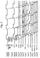
- an external clock signal CLK is input as shown in FIG. 6A and, as a result, signals RAS , CAS , WE and CS are input at a rising edge of the external clock signal CLK to show a read command as shown in FIG. 6B.
- an internal clock signal ICLK1 is generated in synchronization with the external clock signal CLK, and also, an external address signal ADD as shown in FIG. 6C becomes an internal address signal IADD as shown in FIG. 6E.
- the command decoder 7 Upon receiving the read command, the command decoder 7 outputs high level signals READ1 and READ2 as shown in FIGS. 6F and 6G in synchronization with the internal clock signal ICLK1.
- the signal READ1 is brought to a low level in synchronization with the next rising edge of the internal clock signal ICLK1.
- the burst counter 8 Upon receiving the high level signal READ1, the burst counter 8 latches and outputs an internal address signal IADD as shown in FIG. 6H. Thereafter, the signal READ1 goes to a low level, so that the burst counter 8 proceeds to a burst operation, where it generates IADD+1, IADD+2, ... in synchronization with the internal clock signal ICLK1. More specifically, a column address signal YADD is changed to IADD, IADD+1, IADD+2, ⁇ and, as a result, the column decoder 9 sequentially selects column switch lines that correspond to IADD, IADD+1, IADD+2, ⁇ respectively as shown in FIG. 6I. Thus, as shown in FIG. 6N, data are output from the sense amplifiers that have amplified in advance cell data to the read bus RBUS11, RBUS12, ⁇ .
- the internal clock generation circuit 13-B that receives the high level signal READ2 generates an internal clock signal ICLK2 that is synchronized with the internal clock signal ICLK1, as shown in FIG. 6J and outputs internal clock signal ICLK3 that is synchronized only with the rising edge of the internal clock signal ICLK2, as shown in FIG. 6K.
- the frequency of the internal clock signal ICLK3 is equal to 1/2 of that of the internal clock signal ICLK2.
- the data amplifier activation signals DE1 and DE2 are activated immediately after a rising edge and a falling edge of the internal clock signal ICLK3.
- the data on the read bus RBUS11 (12, ) is output to the read bus RBUS21 (22, ... ) in synchronization with the data amplifier activation signal DE1 (DE2, ... ).
- the data on the read bus RBUS21 (22, ⁇ ) is output to the output terminal DOUT1 (DOUT2, ... ).
- FIG. 7 illustrates a second embodiment of the synchronous DRAM device according to the invention, and corresponds to the synchronous DRAM device of FIG. 3.
- the internal clock generation circuit 13-B and the data amplifier activation signal generation circuits 14-1, 14-2, ⁇ of FIG. 5 are replaced by an internal clock generation circuit 13-C and data amplifier activation signal generation circuits 14'-1, 14'-2, ⁇ .
- the internal clock generation circuit 13-C outputs the internal clock signal ICLK3 having a frequency equal to 1/2 of the internal clock signal ICLK1 in synchronization with the internal clock signal ICLK1, it is set and reset according to the internal clock signal ICLK1, the signal READ1 and the signal YADDO.
- the data amplifier activation signal generation circuits 14-1, 14-2, ⁇ output respectively data amplifier activation signals DE1, DE2, ⁇ that are synchronized with either a rising edge or a falling edge of the internal clock signal ICLK3.
- the internal clock generation circuit 13-C is formed by a D-type flip-flop FF' having a set/reset function in place of the D-type flip-flop FF of the internal clock generation circuit 13-B of FIG. 5.
- the D-type flip-flop FF' is set by an AND circuit G4, when the signal READ1 is high the internal clock signal ICLK1 is high and the signal YADDO is high.
- the flip-flop FF' is reset by a gate circuit G5, when the signal READ1 is high, the internal clock signal ICLK1 is high and the signal YADDO is low.
- the internal clock generation circuit 13-C is also enabled by the signal READ2 to divide the frequency of the internal clock signal ICLK1 (ICLK2) by 2 to produce the internal clock signal ICLK3.
- the data activation signal generation circuits 14'-1, 14'-2, ⁇ have configurations that are different from each other.
- the data amplifier activation signal generation circuit 14'-1 includes an AND circuit G6 in place of the exclusive NOR circuit G3 of the data amplifier activation signal generation circuit 14-1 of FIG. 5, whereas the data amplifier activation signal generation circuit 14'-2 includes a NOR circuit G7 in place of the exclusive NOR circuit G3 of the data amplifier activation signal generation circuit 14-2 in FIG. 5.
- the data amplifier activation signal generation circuit 14'-1 generates a constant width pulse signal DE1 at each rising edge of the internal clock signal ICLK3, whereas the data amplifier activation signal generation circuit 14'-2 generates a constant width pulse signal DE2 at each falling edge of the internal clock signal ICLK3.
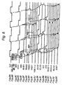
- an external clock signal CLK is input as shown in FIG. 8A and, as a result, signals RAS, CAS, WE and CS are input at a rising edge of the external clock signal CLK to show a read command as shown in FIG. 8B.
- an internal clock signal ICLK1 is generated in synchronization with the external clock signal CLK, and also, an external address signal ADD shown in FIG. 8C becomes an internal address signal IADD as shown in FIG. 8E.
- the command decoder 7 Upon receiving the read command, the command decoder 7 outputs high level signals READ1 and READ2 as shown in FIGS. 8F and 8G in synchronization with the internal clock signal ICLK1.
- the signal READ1 is brought to a low level in synchronization with the next rising edge of the internal clock signal ICLK1.
- the burst counter 8 Upon receiving the high level signal READ1, the burst counter 8 latches and outputs an internal address signal IADD as shown in FIGS. 8H and 8I. Note that IADD is expressed in terms of (YADDO, YADD1). Thereafter, the signal READ1 goes to a low level, so that the burst counter 8 proceeds to a burst operation, where it generates IADD+1, IADD+2, ⁇ in synchronization with the internal clock signal ICLK1. Also note that IADD+1, IADD+2, ⁇ are expressed in terms of (YADDO, YADD1).
- the column address signal YADD is changed to IADD, IADD+1, IADD+2, and, as a result, the column decoder 9 sequentially selects column switch lines that correspond to the addresses of IADD, IADD+1, IADD+2, ... except for the least significant bit, respectively, as shown in FIG. 8J.
- data are output from the sense amplifiers that have amplified in advance cell data to the read buses RBUS11, RBUS12, ⁇ .
- the D-type flip-flop FF' is initialized according to the internal clock signal ICLK1 and the signal YADDO.
- both the internal clock signal ICLK1 (FIG. 8D) and the signal YADDO (FIG. 8H) are high and, therefore, the D-type flip-flop FF' is set.
- an internal clock signal ICLK3B is brought to a low level, whereas the internal clock signal ICLK3 goes to a high level HIGH as shown in FIG. 8L.
- an internal clock signal ICLK2 that is synchronized with the internal clock signal ICLK1 is internally generated as shown in FIG. 8K, and then, an internal clock signal ICLK3 that is synchronized only with a rising edge of the internal clock signal ICLK2 is output, as shown in FIG. 8L.
- the frequency of the internal clock signal ICLK3 will be 1/2 of that of the internal clock signal ICLK2.
- one of the data amplifier activation signals DE1 and DE2 is activated immediately after either a rising edge or a falling edge of the internal clock signal ICLK3.
- the data on the read bus RBUS11 (12) is output to the read bus RBUS2 in synchronization with the data amplifier activation signal DE1 (DE2).
- the data on the read bus RBUS2 is output to the output terminal DOUT.
- the internal clock generation circuits 13-B and 13-C are designed to respond to a rising edge of the external clock signal CLK, the internal clock generation circuits 13-B and 13-C may alternatively be so designed as to respond to a falling edge of the external clock signal CLK.
- the frequency of the internal clock signal ICLK2 is divided into halves so that the average current flowing through the signal line for the internal clock signal ICLK3 will be about half of its counterpart of the comparable prior art devices. Also, the average current J flowing per unit cross-sectional area of the signal line can be about half of its counterpart. Therefore, the 50% fault time t50' due to electro-migration will show an improvement of four times as expressed by the following formula using equation (1) above and the prior art 50% fault time t50.
- the present invention can effectively prevent any reduction in the life span of signal lines due to electro-migration, and hence can improve the reliability of the device.
Landscapes
- Engineering & Computer Science (AREA)
- Microelectronics & Electronic Packaging (AREA)
- Computer Hardware Design (AREA)
- Dram (AREA)
- Static Random-Access Memory (AREA)
Applications Claiming Priority (3)
| Application Number | Priority Date | Filing Date | Title |
|---|---|---|---|
| JP20012/97 | 1997-01-17 | ||
| JP9020012A JPH10208470A (ja) | 1997-01-17 | 1997-01-17 | 同期型半導体記憶装置 |
| JP2001297 | 1997-01-17 |
Publications (2)
| Publication Number | Publication Date |
|---|---|
| EP0854485A2 true EP0854485A2 (fr) | 1998-07-22 |
| EP0854485A3 EP0854485A3 (fr) | 1999-06-16 |
Family
ID=12015210
Family Applications (1)
| Application Number | Title | Priority Date | Filing Date |
|---|---|---|---|
| EP98100866A Withdrawn EP0854485A3 (fr) | 1997-01-17 | 1998-01-19 | Mémoire synchrone à semiconducteurs capable d'améliorer la charge d'une ligne de signal d'horloge |
Country Status (4)
| Country | Link |
|---|---|
| US (2) | US5881019A (fr) |
| EP (1) | EP0854485A3 (fr) |
| JP (1) | JPH10208470A (fr) |
| KR (1) | KR100337581B1 (fr) |
Cited By (1)
| Publication number | Priority date | Publication date | Assignee | Title |
|---|---|---|---|---|
| EP1017059A1 (fr) * | 1998-12-30 | 2000-07-05 | STMicroelectronics S.r.l. | Procédé de lecture d'une mémoire, en particulier une mémoire non-volatile |
Families Citing this family (11)
| Publication number | Priority date | Publication date | Assignee | Title |
|---|---|---|---|---|
| JP4036531B2 (ja) * | 1998-05-27 | 2008-01-23 | 富士通株式会社 | 半導体集積回路 |
| JP2000030456A (ja) * | 1998-07-14 | 2000-01-28 | Fujitsu Ltd | メモリデバイス |
| KR100296964B1 (ko) * | 1999-06-28 | 2001-11-01 | 박종섭 | 패킷 명령어 구동형 메모리소자 |
| KR100318264B1 (ko) * | 1999-06-28 | 2001-12-24 | 박종섭 | 패킷명령어 구동형 메모리소자의 로드신호 발생회로 |
| US6304104B1 (en) * | 1999-09-13 | 2001-10-16 | Rambus, Inc. | Method and apparatus for reducing worst case power |
| JP4480855B2 (ja) * | 2000-06-08 | 2010-06-16 | 富士通マイクロエレクトロニクス株式会社 | 半導体デバイスを含むモジュール、及びモジュールを含むシステム |
| KR100396885B1 (ko) * | 2000-09-05 | 2003-09-02 | 삼성전자주식회사 | 고주파 클럭 신호의 주파수를 낮추어 어드레스 및커맨드의 동작 주파수로 사용하고 서로 다른 주파수의클럭 신호들을 수신하는 반도체 메모리 장치, 이를포함하는 메모리 모듈 및 시스템 메모리 모듈 |
| JP2002328744A (ja) * | 2001-04-27 | 2002-11-15 | Fujitsu Ltd | 半導体集積回路装置 |
| KR100732280B1 (ko) * | 2001-06-27 | 2007-06-25 | 주식회사 하이닉스반도체 | 메모리 시스템 |
| KR100784920B1 (ko) | 2006-11-15 | 2007-12-11 | 주식회사 하이닉스반도체 | 반도체 메모리 장치의 데이터 입력 회로 |
| JP5579580B2 (ja) * | 2010-11-12 | 2014-08-27 | ピーエスフォー ルクスコ エスエイアールエル | 半導体装置 |
Family Cites Families (16)
| Publication number | Priority date | Publication date | Assignee | Title |
|---|---|---|---|---|
| JPS61148692A (ja) * | 1984-12-24 | 1986-07-07 | Nippon Telegr & Teleph Corp <Ntt> | 記憶装置 |
| JPH0225068A (ja) * | 1988-07-13 | 1990-01-26 | Hitachi Ltd | 半導体記憶装置 |
| DE3832152A1 (de) * | 1988-09-22 | 1990-03-29 | Philips Patentverwaltung | Digitaler frequenzgenerator |
| KR100214435B1 (ko) * | 1990-07-25 | 1999-08-02 | 사와무라 시코 | 동기식 버스트 엑세스 메모리 |
| US5341031A (en) * | 1990-08-27 | 1994-08-23 | Mitsubishi Denki Kabushiki Kaisha | Stable high speed clock generator |
| JPH05235138A (ja) * | 1992-02-19 | 1993-09-10 | Nec Ic Microcomput Syst Ltd | 半導体集積回路 |
| JP2830594B2 (ja) * | 1992-03-26 | 1998-12-02 | 日本電気株式会社 | 半導体メモリ装置 |
| JPH07169276A (ja) * | 1993-12-13 | 1995-07-04 | Toshiba Corp | 同期型メモリ |
| US5402389A (en) * | 1994-03-08 | 1995-03-28 | Motorola, Inc. | Synchronous memory having parallel output data paths |
| FI101833B1 (fi) * | 1994-07-13 | 1998-08-31 | Nokia Telecommunications Oy | Menetelmä ja järjestelmä kaapelointiviiveen automaattiseksi kompensoimiseksi kellosignaalin jakelujärjestelmässä |
| JP3013714B2 (ja) * | 1994-09-28 | 2000-02-28 | 日本電気株式会社 | 半導体記憶装置 |
| JPH08221981A (ja) * | 1994-12-15 | 1996-08-30 | Mitsubishi Electric Corp | 同期型半導体記憶装置 |
| JPH08212778A (ja) * | 1995-02-09 | 1996-08-20 | Mitsubishi Electric Corp | 同期型半導体記憶装置およびそのデータ読出方法 |
| US5821643A (en) * | 1995-08-04 | 1998-10-13 | Lucent Technologies Inc. | Synchronization control scheme for a plurality of switching circuits, method of operation therefor and battery plant employing the same |
| JP3824689B2 (ja) * | 1995-09-05 | 2006-09-20 | 株式会社ルネサステクノロジ | 同期型半導体記憶装置 |
| JPH09116098A (ja) * | 1995-10-17 | 1997-05-02 | Sony Corp | クロック配給装置 |
-
1997
- 1997-01-17 JP JP9020012A patent/JPH10208470A/ja active Pending
-
1998
- 1998-01-16 US US09/008,576 patent/US5881019A/en not_active Expired - Lifetime
- 1998-01-16 KR KR1019980001093A patent/KR100337581B1/ko not_active Expired - Lifetime
- 1998-01-19 EP EP98100866A patent/EP0854485A3/fr not_active Withdrawn
- 1998-12-17 US US09/213,251 patent/US6154080A/en not_active Expired - Lifetime
Cited By (2)
| Publication number | Priority date | Publication date | Assignee | Title |
|---|---|---|---|---|
| EP1017059A1 (fr) * | 1998-12-30 | 2000-07-05 | STMicroelectronics S.r.l. | Procédé de lecture d'une mémoire, en particulier une mémoire non-volatile |
| US6477625B1 (en) | 1998-12-30 | 2002-11-05 | Stmelectronics S.R.L. | Method and system for reading a memory by applying control signals thereto |
Also Published As
| Publication number | Publication date |
|---|---|
| KR19980070546A (ko) | 1998-10-26 |
| US5881019A (en) | 1999-03-09 |
| US6154080A (en) | 2000-11-28 |
| KR100337581B1 (ko) | 2002-10-25 |
| EP0854485A3 (fr) | 1999-06-16 |
| JPH10208470A (ja) | 1998-08-07 |
Similar Documents
| Publication | Publication Date | Title |
|---|---|---|
| US6381194B2 (en) | Output circuit for a double data rate dynamic random access memory, double data rate dynamic random access memory, method of clocking data out from a double data rate dynamic random access memory and method of providing a data strobe signal | |
| US6134180A (en) | Synchronous burst semiconductor memory device | |
| JP4370507B2 (ja) | 半導体集積回路装置 | |
| US6977859B2 (en) | Semiconductor memory device and control method thereof | |
| CN113129958B (zh) | 用于宽时钟频率范围命令路径的设备和方法 | |
| US5881019A (en) | Synchronous semiconductor memory device capable of improving load of clock signal line | |
| JP3177094B2 (ja) | 半導体記憶装置 | |
| JPH07262780A (ja) | 並列出力データ経路を有する同期メモリ | |
| US7031205B2 (en) | Random access memory with post-amble data strobe signal noise rejection | |
| US6597626B2 (en) | Synchronous semiconductor memory device | |
| US20080137462A1 (en) | Two-bit per i/o line write data bus for ddr1 and ddr2 operating modes in a dram | |
| JP2003059267A (ja) | 半導体記憶装置 | |
| US7057965B2 (en) | Method of performing access to a single-port memory device, memory access device, integrated circuit device and method of use of an integrated circuit device | |
| JPH11120769A (ja) | 同期型半導体記憶装置 | |
| US6388939B1 (en) | Dual port sram | |
| US6333890B1 (en) | Memory device with a plurality of common data buses | |
| Lee et al. | A 1.6-Gb/s/pin double data rate SDRAM with wave-pipelined CAS latency control | |
| US6272035B1 (en) | Integrated memory | |
| US6751156B2 (en) | Semiconductor memory system having dynamically delayed timing for high-speed data transfers | |
| JPH09180443A (ja) | 半導体メモリ回路 | |
| EP0468135A2 (fr) | Mémoire dynamique à accès aléatoire et à grande vitesse avec temps de relèvement/de précharge prolongé | |
| CN120656513A (zh) | 存储器及其操作方法、存储器系统、计算机系统 | |
| TW202528948A (zh) | 記憶體晶片和記憶體系統 | |
| WO2005024836A1 (fr) | Dispositif a memoire et procede de lecture de donnees a partir d'un dispositif a memoire | |
| JPS6310517B2 (fr) |
Legal Events
| Date | Code | Title | Description |
|---|---|---|---|
| PUAI | Public reference made under article 153(3) epc to a published international application that has entered the european phase |
Free format text: ORIGINAL CODE: 0009012 |
|
| AK | Designated contracting states |
Kind code of ref document: A2 Designated state(s): DE FR GB |
|
| AX | Request for extension of the european patent |
Free format text: AL;LT;LV;MK;RO;SI |
|
| PUAL | Search report despatched |
Free format text: ORIGINAL CODE: 0009013 |
|
| AK | Designated contracting states |
Kind code of ref document: A3 Designated state(s): AT BE CH DE DK ES FI FR GB GR IE IT LI LU MC NL PT SE |
|
| AX | Request for extension of the european patent |
Free format text: AL;LT;LV;MK;RO;SI |
|
| 17P | Request for examination filed |
Effective date: 19991007 |
|
| AKX | Designation fees paid |
Free format text: DE FR GB |
|
| 17Q | First examination report despatched |
Effective date: 20020417 |
|
| RAP1 | Party data changed (applicant data changed or rights of an application transferred) |
Owner name: NEC ELECTRONICS CORPORATION Owner name: NEC CORPORATION |
|
| STAA | Information on the status of an ep patent application or granted ep patent |
Free format text: STATUS: THE APPLICATION IS DEEMED TO BE WITHDRAWN |
|
| 18D | Application deemed to be withdrawn |
Effective date: 20040622 |