EP0854524A2 - Halbleitervorrichtung aus einer Nitridverbindung und Herstellungsverfahren - Google Patents
Halbleitervorrichtung aus einer Nitridverbindung und Herstellungsverfahren Download PDFInfo
- Publication number
- EP0854524A2 EP0854524A2 EP98300306A EP98300306A EP0854524A2 EP 0854524 A2 EP0854524 A2 EP 0854524A2 EP 98300306 A EP98300306 A EP 98300306A EP 98300306 A EP98300306 A EP 98300306A EP 0854524 A2 EP0854524 A2 EP 0854524A2
- Authority
- EP
- European Patent Office
- Prior art keywords
- group
- nitride semiconductor
- intermediate layer
- group iii
- contact
- Prior art date
- Legal status (The legal status is an assumption and is not a legal conclusion. Google has not performed a legal analysis and makes no representation as to the accuracy of the status listed.)
- Withdrawn
Links
- 239000004065 semiconductor Substances 0.000 title claims abstract description 85
- 238000000034 method Methods 0.000 title claims description 36
- 238000004519 manufacturing process Methods 0.000 title claims description 9
- 150000004767 nitrides Chemical class 0.000 title description 5
- 229910021478 group 5 element Inorganic materials 0.000 claims abstract description 41
- 239000000758 substrate Substances 0.000 claims abstract description 36
- IJGRMHOSHXDMSA-UHFFFAOYSA-N Atomic nitrogen Chemical compound N#N IJGRMHOSHXDMSA-UHFFFAOYSA-N 0.000 claims abstract description 32
- 229910052751 metal Inorganic materials 0.000 claims abstract description 24
- 239000002184 metal Substances 0.000 claims abstract description 24
- 229910052757 nitrogen Inorganic materials 0.000 claims abstract description 16
- 125000004429 atom Chemical group 0.000 claims abstract description 12
- 125000004433 nitrogen atom Chemical group N* 0.000 claims abstract description 11
- 238000009792 diffusion process Methods 0.000 claims description 33
- 239000012535 impurity Substances 0.000 claims description 26
- 239000013078 crystal Substances 0.000 claims description 15
- 230000008569 process Effects 0.000 claims description 13
- 239000011521 glass Substances 0.000 claims description 9
- 239000011777 magnesium Substances 0.000 claims description 9
- 238000000151 deposition Methods 0.000 claims description 7
- 150000002500 ions Chemical class 0.000 claims description 4
- 229910052749 magnesium Inorganic materials 0.000 claims description 4
- FYYHWMGAXLPEAU-UHFFFAOYSA-N Magnesium Chemical compound [Mg] FYYHWMGAXLPEAU-UHFFFAOYSA-N 0.000 claims description 3
- 229910045601 alloy Inorganic materials 0.000 claims description 3
- 239000000956 alloy Substances 0.000 claims description 3
- 229910052725 zinc Inorganic materials 0.000 claims description 3
- HCHKCACWOHOZIP-UHFFFAOYSA-N Zinc Chemical compound [Zn] HCHKCACWOHOZIP-UHFFFAOYSA-N 0.000 claims 2
- 239000011701 zinc Substances 0.000 claims 2
- 238000002513 implantation Methods 0.000 claims 1
- JMASRVWKEDWRBT-UHFFFAOYSA-N Gallium nitride Chemical compound [Ga]#N JMASRVWKEDWRBT-UHFFFAOYSA-N 0.000 description 57
- 229910002601 GaN Inorganic materials 0.000 description 54
- 239000000463 material Substances 0.000 description 13
- 229910052698 phosphorus Inorganic materials 0.000 description 12
- OAICVXFJPJFONN-UHFFFAOYSA-N Phosphorus Chemical compound [P] OAICVXFJPJFONN-UHFFFAOYSA-N 0.000 description 11
- 239000000370 acceptor Substances 0.000 description 11
- 239000011574 phosphorus Substances 0.000 description 11
- 230000004888 barrier function Effects 0.000 description 10
- 230000007423 decrease Effects 0.000 description 7
- PXHVJJICTQNCMI-UHFFFAOYSA-N Nickel Chemical compound [Ni] PXHVJJICTQNCMI-UHFFFAOYSA-N 0.000 description 6
- 230000004913 activation Effects 0.000 description 5
- 238000012360 testing method Methods 0.000 description 5
- 238000000137 annealing Methods 0.000 description 4
- 230000015556 catabolic process Effects 0.000 description 4
- 238000006731 degradation reaction Methods 0.000 description 4
- 230000000694 effects Effects 0.000 description 4
- 239000010931 gold Substances 0.000 description 4
- 238000012545 processing Methods 0.000 description 4
- JBRZTFJDHDCESZ-UHFFFAOYSA-N AsGa Chemical compound [As]#[Ga] JBRZTFJDHDCESZ-UHFFFAOYSA-N 0.000 description 3
- 229910001218 Gallium arsenide Inorganic materials 0.000 description 3
- 230000000052 comparative effect Effects 0.000 description 3
- 238000010586 diagram Methods 0.000 description 3
- 238000005452 bending Methods 0.000 description 2
- 230000005540 biological transmission Effects 0.000 description 2
- 238000005253 cladding Methods 0.000 description 2
- 238000005516 engineering process Methods 0.000 description 2
- PCHJSUWPFVWCPO-UHFFFAOYSA-N gold Chemical compound [Au] PCHJSUWPFVWCPO-UHFFFAOYSA-N 0.000 description 2
- 229910052737 gold Inorganic materials 0.000 description 2
- 229910052738 indium Inorganic materials 0.000 description 2
- APFVFJFRJDLVQX-UHFFFAOYSA-N indium atom Chemical compound [In] APFVFJFRJDLVQX-UHFFFAOYSA-N 0.000 description 2
- 238000005259 measurement Methods 0.000 description 2
- 229910052759 nickel Inorganic materials 0.000 description 2
- 230000003287 optical effect Effects 0.000 description 2
- 230000003071 parasitic effect Effects 0.000 description 2
- 125000004437 phosphorous atom Chemical group 0.000 description 2
- 230000009467 reduction Effects 0.000 description 2
- 238000003860 storage Methods 0.000 description 2
- KRHYYFGTRYWZRS-UHFFFAOYSA-N Fluorane Chemical compound F KRHYYFGTRYWZRS-UHFFFAOYSA-N 0.000 description 1
- GYHNNYVSQQEPJS-UHFFFAOYSA-N Gallium Chemical compound [Ga] GYHNNYVSQQEPJS-UHFFFAOYSA-N 0.000 description 1
- 229910017706 MgZn Inorganic materials 0.000 description 1
- 230000003213 activating effect Effects 0.000 description 1
- RNQKDQAVIXDKAG-UHFFFAOYSA-N aluminum gallium Chemical compound [Al].[Ga] RNQKDQAVIXDKAG-UHFFFAOYSA-N 0.000 description 1
- AJGDITRVXRPLBY-UHFFFAOYSA-N aluminum indium Chemical compound [Al].[In] AJGDITRVXRPLBY-UHFFFAOYSA-N 0.000 description 1
- 229910052787 antimony Inorganic materials 0.000 description 1
- 229910052785 arsenic Inorganic materials 0.000 description 1
- 230000009286 beneficial effect Effects 0.000 description 1
- 238000004364 calculation method Methods 0.000 description 1
- 150000001875 compounds Chemical class 0.000 description 1
- 239000000470 constituent Substances 0.000 description 1
- 230000003247 decreasing effect Effects 0.000 description 1
- 230000004069 differentiation Effects 0.000 description 1
- 239000002019 doping agent Substances 0.000 description 1
- 238000002474 experimental method Methods 0.000 description 1
- 230000002349 favourable effect Effects 0.000 description 1
- 230000005669 field effect Effects 0.000 description 1
- 229910052733 gallium Inorganic materials 0.000 description 1
- 230000017525 heat dissipation Effects 0.000 description 1
- 229910000040 hydrogen fluoride Inorganic materials 0.000 description 1
- 230000010354 integration Effects 0.000 description 1
- 238000012986 modification Methods 0.000 description 1
- 230000004048 modification Effects 0.000 description 1
- 230000036961 partial effect Effects 0.000 description 1
- 229910052594 sapphire Inorganic materials 0.000 description 1
- 239000010980 sapphire Substances 0.000 description 1
- 239000002904 solvent Substances 0.000 description 1
- 238000006467 substitution reaction Methods 0.000 description 1
- 230000036964 tight binding Effects 0.000 description 1
- 230000000699 topical effect Effects 0.000 description 1
Images


Classifications
-
- H—ELECTRICITY
- H10—SEMICONDUCTOR DEVICES; ELECTRIC SOLID-STATE DEVICES NOT OTHERWISE PROVIDED FOR
- H10H—INORGANIC LIGHT-EMITTING SEMICONDUCTOR DEVICES HAVING POTENTIAL BARRIERS
- H10H20/00—Individual inorganic light-emitting semiconductor devices having potential barriers, e.g. light-emitting diodes [LED]
- H10H20/80—Constructional details
- H10H20/83—Electrodes
- H10H20/832—Electrodes characterised by their material
-
- H—ELECTRICITY
- H10—SEMICONDUCTOR DEVICES; ELECTRIC SOLID-STATE DEVICES NOT OTHERWISE PROVIDED FOR
- H10H—INORGANIC LIGHT-EMITTING SEMICONDUCTOR DEVICES HAVING POTENTIAL BARRIERS
- H10H20/00—Individual inorganic light-emitting semiconductor devices having potential barriers, e.g. light-emitting diodes [LED]
- H10H20/80—Constructional details
- H10H20/81—Bodies
- H10H20/822—Materials of the light-emitting regions
- H10H20/824—Materials of the light-emitting regions comprising only Group III-V materials, e.g. GaP
- H10H20/825—Materials of the light-emitting regions comprising only Group III-V materials, e.g. GaP containing nitrogen, e.g. GaN
- H10H20/8252—Materials of the light-emitting regions comprising only Group III-V materials, e.g. GaP containing nitrogen, e.g. GaN characterised by the dopants
-
- H—ELECTRICITY
- H01—ELECTRIC ELEMENTS
- H01S—DEVICES USING THE PROCESS OF LIGHT AMPLIFICATION BY STIMULATED EMISSION OF RADIATION [LASER] TO AMPLIFY OR GENERATE LIGHT; DEVICES USING STIMULATED EMISSION OF ELECTROMAGNETIC RADIATION IN WAVE RANGES OTHER THAN OPTICAL
- H01S5/00—Semiconductor lasers
- H01S5/30—Structure or shape of the active region; Materials used for the active region
- H01S5/32—Structure or shape of the active region; Materials used for the active region comprising PN junctions, e.g. hetero- or double- heterostructures
- H01S5/323—Structure or shape of the active region; Materials used for the active region comprising PN junctions, e.g. hetero- or double- heterostructures in AIIIBV compounds, e.g. AlGaAs-laser, InP-based laser
- H01S5/32308—Structure or shape of the active region; Materials used for the active region comprising PN junctions, e.g. hetero- or double- heterostructures in AIIIBV compounds, e.g. AlGaAs-laser, InP-based laser emitting light at a wavelength less than 900 nm
- H01S5/32341—Structure or shape of the active region; Materials used for the active region comprising PN junctions, e.g. hetero- or double- heterostructures in AIIIBV compounds, e.g. AlGaAs-laser, InP-based laser emitting light at a wavelength less than 900 nm blue laser based on GaN or GaP
-
- H—ELECTRICITY
- H10—SEMICONDUCTOR DEVICES; ELECTRIC SOLID-STATE DEVICES NOT OTHERWISE PROVIDED FOR
- H10H—INORGANIC LIGHT-EMITTING SEMICONDUCTOR DEVICES HAVING POTENTIAL BARRIERS
- H10H20/00—Individual inorganic light-emitting semiconductor devices having potential barriers, e.g. light-emitting diodes [LED]
- H10H20/80—Constructional details
- H10H20/84—Coatings, e.g. passivation layers or antireflective coatings
Definitions
- the invention relates to a semiconductor device and a method of fabricating such a device, and particularly relates to a p-type Group III-nitride semiconductor device that has a low voltage-drop p-contact and a method of fabricating such a device.
- Group III-nitride compound semiconductors are promising materials for use in making semiconductor light-emitting devices, such as semiconductor lasers and semiconductor light-emitting diodes. Such compound semiconductors are also promising for use in making such circuit devices as metal semiconductor field-effect transistors (MESFETs).
- semiconductor lasers based on such Group III-nitride compound semiconductors such as gallium nitride (GaN), aluminum gallium nitride (AIGaN), indium gallium nitride (InGaN) or aluminum indium gallium nitride (AllnGaN) have great potential for generating light in the blue and violet wavelength ranges due to their substantially wider band gap than gallium arsenide, the material used to make lasers that emit red light.
- a semiconductor material that includes at least gallium and nitrogen will be referred to in this disclosure as a gallium nitride semiconductor.
- a semiconductor that includes at least one Group III element and at least nitrogen will be called a Group III-nitride semiconductor.
- a semiconductor device that includes a Group III-nitride semiconductor will be called a Group III-nitride semiconductor device.
- Figure 1 shows an example of an edge-emitting semiconductor laser 1 based on gallium nitride semiconductors.
- This device is formed by depositing the GaN buffer layer 3 on the sapphire substrate 2, and then successively depositing the n-type GaN contact layer 4, the n-type AIGaN cladding layer 6, the GaN waveguide layer 7, the InGaN multi-quantum well layer 8, the p-type GaN waveguide layer 9, the p-type AIGaN cladding layer 10, and the p-type GaN contact layer 11.
- the n-contact 13 is formed by dispositing the metal n electrode 5 on the n-type GaN contact layer 4 and the p-contact 14 is formed by depositing the metal p electrode 12 on the p-type GaN contact layer 11.
- the contact resistance of the n-contact 13 is acceptably small.
- the contact resistance of the p-contact 14 between the p-type GaN contact layer 1 1 and the p electrode 12 is large.
- the p electrode is formed from layers of gold and nickel and contacts an approximately 100 ⁇ m 100 ⁇ m area of the p-type GaN contact layer 11. Even if the specific contact resistance between the p electrode and the contact layer can be reduced to as little as 2 ⁇ 10 -1 ⁇ cm 2 , the p-contact has a contact resistance of 2,000 ⁇ . Consequently, a drive current of 100 mA will dissipate about 20 W of power at the p-contact.
- the high contact resistance of the p-contact increases parasitic resistance, increases power consumption, and increases device temperature.
- the high contact resistance of the p-contact degrades the performance of essential functions of the semiconductor device, and shortens the life of the device. Therefore, a decrease in the contact resistance of the p-contact is sought.
- a p-contact or n-contact is a metal-to-semiconductor contact with a contact resistance that is sufficiently small that the contact resistance can be ignored compared with the bulk resistance of the semiconductor in series with the contact.
- the performance of a resistive contact can be characterized by its specific contact resistance, Rc.
- the specific contact resistance Rc depends exponentially on ⁇ B N -1 ⁇ 2 , so increasing the impurity concentration N is also effective to decrease the specific contact resistance.
- the impurity concentration in the p-type GaN is believed to be about ten times greater than 10 18 cm -3 .
- Such high impurity concentrations in p-type GaN result in a significant drop in the activation rate of the acceptors or in an extreme degradation of crystallinity, so favorable results are not obtained.
- M.E. Lin et al. disclose an example of depositing electrodes composed of two layers of Ti/AI on n-type GaN and annealing at 900°C for a short time of 30 seconds to obtain a specific contact resistance of 8 x 10 -6 ⁇ .cm 2 .
- This paper also discloses an example of depositing an InN/GaN short-period superlattice (SPS) on a GaN layer and depositing a highly-doped InN layer on the SPS structure as a cap layer.
- SPS InN/GaN short-period superlattice
- a metal electrode is deposited on the cap layer.
- This structure provides a contact with a specific contact resistance of 8 x 10 -5 ⁇ .cm 2 without annealing.
- the quantum tunnel effect passing through the SPS conduction band is thought to narrow the effective band gap.
- Figure 2 shows a schematic band diagram of the contact described in the article.
- n-type lnN and n-type GaN were alternately deposited in layers on an n-type GaN layer.
- the impurity level of the n-type GaN of the GaN layer and in the SPS was 5 ⁇ 10 18 cm -3 .
- the impurity level of the n-type InN of the cap layer and in the SPS was 1 ⁇ 10 19 cm -3 , so the metal-semiconductor structure whose band diagram is shown in Figure 2 has no ability to function as a rectifier.
- ln x Ga 1-x AS is used as a cap layer to which the p-contact is made.
- ln x Ga 1-x N is a potential material for such a cap layer, but since the In content of the ln x Ga 1-x N has a relatively small bending effect on the band gap, ln x Ga 1-x N with a large In fraction must be used to narrow the band gap significantly. Diffusing In into GaN to form ln x Ga 1-x N with a large In fraction is difficult in itself, and additionally causes problems due to the large lattice mismatch between ln x Ga 1-x N and GaN.
- a p-contact with an acceptably-low specific contact resistance can be fabricated inexpensively on p-type GaN, and can provide better reliability, the possibility exists that a similar contact structure can be applied to other p-type Group III-nitride semiconductor devices and not just to p-type gallium nitride semiconductor devices.
- a p-type Group III-nitride semiconductor device that has a p-contact with a low Schottky barrier and a low specific contact resistance.
- the invention provides a Group III-nitride semiconductor device that has a low voltage-drop p-contact and that comprises a substrate layer, a metal electrode and an intermediate layer sandwiched between the substrate layer and the metal electrode.
- the substrate layer is a layer of a p-type Group III-nitride semiconductor
- the intermediate layer includes a Group III-nitride semiconductor in which atoms of a Group V element other than nitrogen have been substituted for a fraction of nitrogen atoms.
- the invention also provides a method of fabricating a Group III-nitride semiconductor device that has a low voltage-drop p-contact.
- a substrate including a p-type Group III-nitride semiconductor having an exposed surface is provided.
- Atoms of a Group V element other than nitrogen are substituted for a fraction of the nitrogen atoms of the p-type Group III-nitride semiconductor to form an intermediate layer extending into the p-type Group III-nitride semiconductor from the exposed surface.
- Metal is then deposited on the exposed surface to form an electrode in electrical contact with the intermediate layer.
- Figure 3 shows a cross-sectional view of the edge-emitting Group III-nitride semiconductor laser 100 as an example of a Group III-nitride semiconductor device incorporating the low specific contact resistance p-contact of the invention.
- Elements of the laser 100 that are the same as those in the laser 1 shown in Figure 1 are indicated by the same reference numerals and will not be described again here.
- the p-contact 110 includes the metal p electrode 12, the p-type GaN contact layer 11, and the intermediate layer 112.
- the intermediate layer is part of the contact layer of p-type Group-III nitride semiconductor in which atoms of a Group V element other than nitrogen are substituted for a fraction of the nitrogen atoms of the p-type Group III-nitride semiconductor, i.e., the intermediate layer includes p-type IIIN 1-x V x , where III is at least one element of Group III, V is at least one element of Group V other than nitrogen, and 0 ⁇ x ⁇ 1.
- the intermediate layer is a layer of gallium nitride phosphide GaN 1 _ x P x in which 0 ⁇ x ⁇ 1.
- gallium nitride can easily be doped with phosphorus. Moroever, as noted above, phosphorus has a large bending effect on the band gap of gallium nitride. Therefore, selecting the appropriate value of x in GaN 1- x P x has the potential to reduce the height of the Schottky barrier between the p-contact and the intermediate layer sandwiched between the p-type GaN and the p electrode, and to reduce the specific contact resistance of the p-contact.
- the band structure of GaN 1-x P x depends on the value of x.
- An initial value of x may be selected by considering the effect of the value of x on the band structure of the semiconductor, and may be optimized by subsequent experiments to obtain the value of x that provides the lowest voltage drop for a given device current.
- the band gap decreases with increasing x, and reaches a minimum at x ⁇ 0.5.
- Crystals with values of x ⁇ 0.1 are easier to produce with good crystal uniformity and x-homogeneity, and a beneficial reduction in the voltage drop across the p-contact is obtained with a value of x as low as 0.01.
- the preferred range of x is 0.01 ⁇ x ⁇ 0.5.
- step 40 a p-type gallium nitride substrate doped with magnesium as the acceptor impurity is provided.
- step 42 a solution containing PSG is spincoated onto the surface of the p-type GaN substrate.
- the substrate is baked for 3.5 hours at 110°C to evaporate the solvent from the solution. This leaves the surface of the substrate coated with PSG.
- step 48A the substrate is baked at a temperature of 900° C for 5 minutes. This activates the Mg dopant in the GaN and additionally causes phosphorus to diffuse from the PSG into the substrate to form the intermediate layer.
- step 50A the substrate is etched in HF to remove the PSG layer from the surface of the substrate.
- step 52 a one nm-thick layer of nickel and a 200 nm-thick layer of gold are vapor deposited on the surface of intermediate layer, which constitutes the surface of the substrate, to form the p electrode.
- step 58 the specific contact resistance of the improved p-contact formed by the method according to the invention is measured. The process then ends.
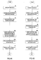
- FIG. 4B The method for fabricating a reference element incorporating a conventional p-contact for use in comparative tests will now be described with reference to Figure 4B.
- the process illustrated in Figure 4B forms a p-contact in which no intermediate layer is sandwiched between the metal electrode and the p-type GaN substrate. Steps in the process illustrated in Figure 4B that are identical to the process illustrated in Figure 4A are indicated by the same reference numeral and will not be described again here.
- step 46 the substrate is etched in hydrogen fluoride HF to remove the PSG layer. Consequently, the high-temperature bake performed in next step 48B activates the acceptor impurities in the substrate, but no phosphorus diffuses into the substrate. Hence, no intermediate layer is formed.
- the HF etch step performed next in step 50B removes a surface oxide film from the exposed surface of the substrate, but does not remove the PSG layer, since this was removed in step 46.
- the specific contact resistance of the elements made by the processes shown in Figures 4A and 4B are measured after fabrication and prior to annealing. As is well known, annealing decreases the value of the specific contact resistance by a factor of about ten.
- Electrodes with a short side of 75 ⁇ m and a long side of 0.50 mm are formed on the surfaces of both the reference element and the improved element.
- the long sides of the electrodes are parallel to one another and to the short sides of the substrate.
- the distance between adjacent electrodes varies from 25 am to 175 am in 25 ⁇ m steps. This arrangement of electrodes enables the contact resistance of the p-contact according to the invention to be compared with that of the conventional p-contact using the transmission line method. Current is passed between adjacent pairs of the electrodes and the voltage drop between the electrodes to the current passing is measured.
- Figure 5 shows one example of the current and voltage characteristics.
- Curve A represents the current/voltage characteristic of the conventional p-contact.
- Curve B represents the characteristics of the p-contact according to the invention.
- the measurement current is the total current flowing between the electrodes.
- the maximum current density of the current flowing through the p-contact between the electrodes has a value of several kA/cm 2 in the shortest current path between the electrodes.
- the p-contact according to the invention has a lower DC resistance due to the significantly lower Schottky barrier in the p-contact according to the invention.
- the value of the specific contact resistance determined by using the above measurements in a transmission line model is 1.6 ⁇ 10 -1 ⁇ .cm 2 in the conventional p-contact and 1.1 ⁇ 10 -1 ⁇ .cm 2 in the p-contact according to the invention. Under these conditions, the specific contact resistance of the p-contact according to the invention is significantly less than that of the conventional p-contact.
- the high temperature bake step 48A must be performed at a temperature in the range from 800°C to 1,100°C. Preferably, this step is performed at a temperature between 850°C and 950°C.
- this step is performed at a temperature between 850°C and 950°C.
- degradation of the crystallinity of the substrate caused by high temperature, acceptor activation in the GaN:Mg, and phosphorus diffusion from the PSG occur simultaneously. Consequently, all three of these factors should be considered when determining the conditions for performing the high-temperature bake step 48A.
- the high-temperature bake step should be performed at a low temperature for a short time.
- the high-temperature bake step should be performed at a high temperature for a long time.
- the high-temperature bake step should be performed at a high temperature for a relatively short time. For optimum results, the conditions of the high-temperature bake step should be selected so that these conflicting factors are balanced.
- the optimum conditions for acceptor activation are obtained, and the optimum phosphorus diffusion is simultaneously achieved by performing the high-temperature bake step for 5 minutes at a temperature of 900°C.
- the resulting acceptor concentration is 2 ⁇ 10 17 cm -3 .
- the value of x in the GaN 1 _ x P x mixed crystal of the intermediate layer is assumed to be in the range from 0.01 and no more than 0.5.
- phosphorus atoms thermally diffusing from the PSG replace a fraction of the nitrogen atoms of the p-type gallium nitride to form the intermediate layer composed of GaNP mixed crystal.
- the intermediate layer can alternatively be formed by thermally diffusing atoms of another Group V element other than nitrogen from glass containing that element.
- GaNPAsSb mixed crystal, GaNP mixed crystal, GaNAs mixed crystal, or GaNSb mixed crystal are the preferred constituents of the material of the intermediate layer.
- the Group V elements that may be substituted for nitrogen in the gallium nitride material have increasing atomic weights in the order of P, As, and Sb. Since the diffusion rate decreases as the atomic weight increases, the diffusion process must be performed at a higher temperature for a longer time to obtain a predetermined concentration of substitute Group V atoms. On the other hand, the concentration of the substituted element required to produce a specific reduction in the band gap decreases as the atomic weight of the substitution element increases. Consequently, favorably maintaining crystallinity is balanced with simultaneously fostering acceptor activation. The inventor prefers to use essentially the same temperature and time in the high-temperature bake step as are used with phosphorus.
- the way in which the mixed crystal of the intermediate layer is formed is not limited to thermal diffusion from glass.
- Alternative methods include:
- thermally diffusing the Group V element is preferred.
- a further decrease in the specific contact resistance and improved reliability can be expected by doping the intermediate layer with a Group II element impurity.
- the energy level of the valence band in the intermediate layer can be raised and the height of the Schottky barrier between the metal electrode and the substrate can be lowered by doping the gallium nitride material of the substrate with a Group V element other than nitrogen to form the intermediate layer, as described above.
- the Schottky barrier can be narrowed by doping the intermediate layer with an acceptor impurity such as a Group II element. Narrowing the Schottky barrier increases the tunnelling current between the metal and the intermediate layer and provides a lower specific contact resistance.
- Suitable Group II elements that can be used to dope the intermediate layer are Mg, Zn, and MgZn. Doping the intermediate layer narrows the Schottky barrier and additionally increases the acceptor concentration in the p-type GaN substrate.
- the intermediate layer can be doped with the Group II element using one of several possible methods, some of which correspond to the doping methods listed above for doping the substrate with the Group V element to form the intermediate layer.
- possible doping methods for the Group II impurities include thermal diffusion from glass containing the Group II element, thermal diffusion from an atmosphere containing the Group II element, thermal diffusion from a solution of the Group II element in a molten Group III element, implanting ions of the Group II element into the surface of the substrate, introducing the Group II element while the intermediate layer is epitaxially grown, and thermal diffusion from a multilayered metal film containing the Group II element or from an alloy containing the Group II element.
- thermal diffusion of the Group II impurities may either precede or follow thermal diffusion of the Group V element.
- the method based on thermal diffusion from glass is considered to be optimal. In other circumstances, another of the methods can be optimal.
- a p-contact according to the invention in which an intermediate layer is sandwiched between a p-type Group III-nitride semiconductor and a metal electrode has a low specific contact resistance.
- the material of the intermediate layer is a p-type Group III-nitride semiconductor in which atoms of a Group V element other than nitrogen have been substituted for a fraction of the nitrogen atoms of the p-type Group III-nitride semiconductor.
- a semiconductor device incorporating the p-contact according to the invention has a reduced power consumption, higher efficiency and lower parasitic resistance.
- the method according to the invention of fabricating a p-contact for Group III nitride semiconductors allows a variety of processing conditions. Therefore, processing conditions that are most compatible with the processing used to fabricate the remainder of the semiconductor device, the available materials, and the technology level can be selected. This simplifies implementation of the fabrication method.
Landscapes
- Electrodes Of Semiconductors (AREA)
- Semiconductor Lasers (AREA)
- Led Devices (AREA)
Applications Claiming Priority (2)
| Application Number | Priority Date | Filing Date | Title |
|---|---|---|---|
| JP533997A JPH10209569A (ja) | 1997-01-16 | 1997-01-16 | p型窒化物半導体装置とその製造方法 |
| JP5339/97 | 1997-01-16 |
Publications (2)
| Publication Number | Publication Date |
|---|---|
| EP0854524A2 true EP0854524A2 (de) | 1998-07-22 |
| EP0854524A3 EP0854524A3 (de) | 1998-12-16 |
Family
ID=11608478
Family Applications (1)
| Application Number | Title | Priority Date | Filing Date |
|---|---|---|---|
| EP98300306A Withdrawn EP0854524A3 (de) | 1997-01-16 | 1998-01-16 | Halbleitervorrichtung aus einer Nitridverbindung und Herstellungsverfahren |
Country Status (3)
| Country | Link |
|---|---|
| US (2) | US6150672A (de) |
| EP (1) | EP0854524A3 (de) |
| JP (1) | JPH10209569A (de) |
Cited By (1)
| Publication number | Priority date | Publication date | Assignee | Title |
|---|---|---|---|---|
| EP2262012B1 (de) * | 2008-04-02 | 2017-12-27 | LG Innotek Co., Ltd. | Leuchtdiode und herstellungsverfahren dafür |
Families Citing this family (35)
| Publication number | Priority date | Publication date | Assignee | Title |
|---|---|---|---|---|
| JPH10209569A (ja) * | 1997-01-16 | 1998-08-07 | Hewlett Packard Co <Hp> | p型窒化物半導体装置とその製造方法 |
| JP3469484B2 (ja) * | 1998-12-24 | 2003-11-25 | 株式会社東芝 | 半導体発光素子およびその製造方法 |
| KR100308921B1 (ko) * | 1999-03-17 | 2001-09-26 | 김효근 | p형 GaN계 반도체의 낮은 오믹 접촉 저항 형성을 위한 Epi구조 및 낮은 오믹접촉 저항 형성을 위한 Epi 구조 성장방법 |
| JP3609661B2 (ja) * | 1999-08-19 | 2005-01-12 | 株式会社東芝 | 半導体発光素子 |
| JP4315583B2 (ja) * | 2000-09-19 | 2009-08-19 | パイオニア株式会社 | Iii族窒化物系半導体レーザ素子 |
| US6541799B2 (en) * | 2001-02-20 | 2003-04-01 | Showa Denko K.K. | Group-III nitride semiconductor light-emitting diode |
| JP2002289955A (ja) * | 2001-03-23 | 2002-10-04 | Sharp Corp | 半導体レーザ素子とその製造方法および光学式情報再生装置 |
| US6958497B2 (en) * | 2001-05-30 | 2005-10-25 | Cree, Inc. | Group III nitride based light emitting diode structures with a quantum well and superlattice, group III nitride based quantum well structures and group III nitride based superlattice structures |
| US7692182B2 (en) * | 2001-05-30 | 2010-04-06 | Cree, Inc. | Group III nitride based quantum well light emitting device structures with an indium containing capping structure |
| US6709989B2 (en) | 2001-06-21 | 2004-03-23 | Motorola, Inc. | Method for fabricating a semiconductor structure including a metal oxide interface with silicon |
| US20030015708A1 (en) * | 2001-07-23 | 2003-01-23 | Primit Parikh | Gallium nitride based diodes with low forward voltage and low reverse current operation |
| US6878975B2 (en) * | 2002-02-08 | 2005-04-12 | Agilent Technologies, Inc. | Polarization field enhanced tunnel structures |
| US7084423B2 (en) | 2002-08-12 | 2006-08-01 | Acorn Technologies, Inc. | Method for depinning the Fermi level of a semiconductor at an electrical junction and devices incorporating such junctions |
| US6833556B2 (en) | 2002-08-12 | 2004-12-21 | Acorn Technologies, Inc. | Insulated gate field effect transistor having passivated schottky barriers to the channel |
| KR100882977B1 (ko) * | 2003-03-03 | 2009-02-12 | 엘지전자 주식회사 | 발광 소자 제조 방법 |
| US7534633B2 (en) | 2004-07-02 | 2009-05-19 | Cree, Inc. | LED with substrate modifications for enhanced light extraction and method of making same |
| JP4639107B2 (ja) * | 2005-03-31 | 2011-02-23 | 富士通株式会社 | 半導体レーザ及びその製造方法 |
| US20060262243A1 (en) * | 2005-05-19 | 2006-11-23 | Lester Steven D | Display system and method using a solid state laser |
| US20060267043A1 (en) * | 2005-05-27 | 2006-11-30 | Emerson David T | Deep ultraviolet light emitting devices and methods of fabricating deep ultraviolet light emitting devices |
| JP4956924B2 (ja) * | 2005-06-29 | 2012-06-20 | 豊田合成株式会社 | 半導体デバイス、及びその電極の製造方法 |
| US8519437B2 (en) * | 2007-09-14 | 2013-08-27 | Cree, Inc. | Polarization doping in nitride based diodes |
| US9012937B2 (en) | 2007-10-10 | 2015-04-21 | Cree, Inc. | Multiple conversion material light emitting diode package and method of fabricating same |
| US9287469B2 (en) * | 2008-05-02 | 2016-03-15 | Cree, Inc. | Encapsulation for phosphor-converted white light emitting diode |
| US8415692B2 (en) | 2009-07-06 | 2013-04-09 | Cree, Inc. | LED packages with scattering particle regions |
| US8536615B1 (en) | 2009-12-16 | 2013-09-17 | Cree, Inc. | Semiconductor device structures with modulated and delta doping and related methods |
| US8604461B2 (en) | 2009-12-16 | 2013-12-10 | Cree, Inc. | Semiconductor device structures with modulated doping and related methods |
| US8575592B2 (en) * | 2010-02-03 | 2013-11-05 | Cree, Inc. | Group III nitride based light emitting diode structures with multiple quantum well structures having varying well thicknesses |
| KR100969131B1 (ko) * | 2010-03-05 | 2010-07-07 | 엘지이노텍 주식회사 | 발광 소자 제조방법 |
| US8557693B2 (en) | 2010-06-03 | 2013-10-15 | International Business Machines Corporation | Contact resistivity reduction in transistor devices by deep level impurity formation |
| WO2012016377A1 (en) * | 2010-08-03 | 2012-02-09 | Industrial Technology Research Institute | Light emitting diode chip, light emitting diode package structure, and method for forming the same |
| US8779412B2 (en) * | 2011-07-20 | 2014-07-15 | Samsung Electronics Co., Ltd. | Semiconductor light emitting device |
| CN107578994B (zh) | 2011-11-23 | 2020-10-30 | 阿科恩科技公司 | 通过插入界面原子单层改进与iv族半导体的金属接触 |
| US9620611B1 (en) | 2016-06-17 | 2017-04-11 | Acorn Technology, Inc. | MIS contact structure with metal oxide conductor |
| DE112017005855T5 (de) | 2016-11-18 | 2019-08-01 | Acorn Technologies, Inc. | Nanodrahttransistor mit Source und Drain induziert durch elektrische Kontakte mit negativer Schottky-Barrierenhöhe |
| JP6940866B2 (ja) * | 2017-06-21 | 2021-09-29 | 国立研究開発法人情報通信研究機構 | 半導体光デバイス、半導体光源、光集積回路、及び半導体光デバイスの製造方法 |
Family Cites Families (9)
| Publication number | Priority date | Publication date | Assignee | Title |
|---|---|---|---|---|
| US5689123A (en) * | 1994-04-07 | 1997-11-18 | Sdl, Inc. | III-V aresenide-nitride semiconductor materials and devices |
| US5693963A (en) * | 1994-09-19 | 1997-12-02 | Kabushiki Kaisha Toshiba | Compound semiconductor device with nitride |
| JP2666237B2 (ja) * | 1994-09-20 | 1997-10-22 | 豊田合成株式会社 | 3族窒化物半導体発光素子 |
| JP3605906B2 (ja) * | 1994-10-28 | 2004-12-22 | 三菱化学株式会社 | コンタクト抵抗低減層を有する半導体装置 |
| US5804834A (en) * | 1994-10-28 | 1998-09-08 | Mitsubishi Chemical Corporation | Semiconductor device having contact resistance reducing layer |
| JPH08222797A (ja) * | 1995-01-17 | 1996-08-30 | Hewlett Packard Co <Hp> | 半導体装置およびその製造方法 |
| JP3457468B2 (ja) * | 1995-09-12 | 2003-10-20 | 株式会社東芝 | 多層構造半導体装置 |
| US5834331A (en) * | 1996-10-17 | 1998-11-10 | Northwestern University | Method for making III-Nitride laser and detection device |
| JPH10209569A (ja) * | 1997-01-16 | 1998-08-07 | Hewlett Packard Co <Hp> | p型窒化物半導体装置とその製造方法 |
-
1997
- 1997-01-16 JP JP533997A patent/JPH10209569A/ja active Pending
-
1998
- 1998-01-06 US US09/003,259 patent/US6150672A/en not_active Expired - Fee Related
- 1998-01-16 EP EP98300306A patent/EP0854524A3/de not_active Withdrawn
-
2000
- 2000-05-01 US US09/562,494 patent/US6238945B1/en not_active Expired - Fee Related
Cited By (1)
| Publication number | Priority date | Publication date | Assignee | Title |
|---|---|---|---|---|
| EP2262012B1 (de) * | 2008-04-02 | 2017-12-27 | LG Innotek Co., Ltd. | Leuchtdiode und herstellungsverfahren dafür |
Also Published As
| Publication number | Publication date |
|---|---|
| US6150672A (en) | 2000-11-21 |
| JPH10209569A (ja) | 1998-08-07 |
| US6238945B1 (en) | 2001-05-29 |
| EP0854524A3 (de) | 1998-12-16 |
Similar Documents
| Publication | Publication Date | Title |
|---|---|---|
| US6150672A (en) | P-type group III-nitride semiconductor device | |
| KR100912092B1 (ko) | Ⅲ-니트라이드 발광 장치에서 옴 접촉의 형성 | |
| US6169296B1 (en) | Light-emitting diode device | |
| US6100174A (en) | GaN group compound semiconductor device and method for producing the same | |
| Murakami et al. | Ohmic contacts for compound semiconductors | |
| US6239490B1 (en) | P-contact for a Group III-nitride semiconductor device and method of making same | |
| US7915633B2 (en) | Nitride semiconductor device and manufacturing method thereof | |
| US5561080A (en) | Semiconductor laser and method for fabricating the same | |
| US6033929A (en) | Method for making II-VI group compound semiconductor device | |
| US6335219B1 (en) | Nitride semiconductor light-emitting device and manufacturing method of the same | |
| EP0594212A1 (de) | Ohmsche Electrode, Verfahren für ihre Herstellung und lichtemittierende Vorrichtung | |
| KR100293467B1 (ko) | 청색발광소자및그제조방법 | |
| JP3464629B2 (ja) | p型コンタクト電極装置および発光装置 | |
| JPH10242074A (ja) | 窒化物半導体素子製造方法 | |
| US5924002A (en) | Method of manufacturing a semiconductor device having ohmic electrode | |
| US12249628B2 (en) | Method of forming p-type nitride semiconductor layer | |
| JP2001320083A (ja) | AlGaInP系発光素子及び発光素子用エピタキシャルウェハ | |
| JP2893990B2 (ja) | 半導体レーザおよびその作製方法 | |
| JPH08264876A (ja) | 発光素子 | |
| JPH0786697A (ja) | 発光素子 | |
| JPH09107155A (ja) | 半導体発光素子 | |
| JP2001007388A (ja) | AlGaInP発光ダイオード | |
| JPH07193335A (ja) | オーミック電極構造およびそれを用いた発光素子 | |
| JPH0653613A (ja) | 半導体素子 | |
| JPH07321375A (ja) | 半導体発光素子 |
Legal Events
| Date | Code | Title | Description |
|---|---|---|---|
| PUAI | Public reference made under article 153(3) epc to a published international application that has entered the european phase |
Free format text: ORIGINAL CODE: 0009012 |
|
| AK | Designated contracting states |
Kind code of ref document: A2 Designated state(s): DE FR GB |
|
| AX | Request for extension of the european patent |
Free format text: AL;LT;LV;MK;RO;SI |
|
| PUAL | Search report despatched |
Free format text: ORIGINAL CODE: 0009013 |
|
| AK | Designated contracting states |
Kind code of ref document: A3 Designated state(s): AT BE CH DE DK ES FI FR GB GR IE IT LI LU MC NL PT SE |
|
| AX | Request for extension of the european patent |
Free format text: AL;LT;LV;MK;RO;SI |
|
| 17P | Request for examination filed |
Effective date: 19990525 |
|
| AKX | Designation fees paid |
Free format text: DE FR GB |
|
| RAP1 | Party data changed (applicant data changed or rights of an application transferred) |
Owner name: HEWLETT-PACKARD COMPANY, A DELAWARE CORPORATION |
|
| RAP1 | Party data changed (applicant data changed or rights of an application transferred) |
Owner name: AGILENT TECHNOLOGIES INC. |
|
| RAP1 | Party data changed (applicant data changed or rights of an application transferred) |
Owner name: AGILENT TECHNOLOGIES INC. A DELAWARE CORPORATION |
|
| STAA | Information on the status of an ep patent application or granted ep patent |
Free format text: STATUS: THE APPLICATION HAS BEEN WITHDRAWN |
|
| RAP1 | Party data changed (applicant data changed or rights of an application transferred) |
Owner name: AGILENT TECHNOLOGIES, INC. (A DELAWARE CORPORATION |
|
| 18W | Application withdrawn |
Withdrawal date: 20010912 |