EP0855451A1 - Drahtfilm, sputtertarget zur herstellung des drahtfilms und elektronische teile, die diesen verwenden - Google Patents
Drahtfilm, sputtertarget zur herstellung des drahtfilms und elektronische teile, die diesen verwenden Download PDFInfo
- Publication number
- EP0855451A1 EP0855451A1 EP96933629A EP96933629A EP0855451A1 EP 0855451 A1 EP0855451 A1 EP 0855451A1 EP 96933629 A EP96933629 A EP 96933629A EP 96933629 A EP96933629 A EP 96933629A EP 0855451 A1 EP0855451 A1 EP 0855451A1
- Authority
- EP
- European Patent Office
- Prior art keywords
- thin film
- interconnector line
- interconnector
- line
- intermetallic compound
- Prior art date
- Legal status (The legal status is an assumption and is not a legal conclusion. Google has not performed a legal analysis and makes no representation as to the accuracy of the status listed.)
- Withdrawn
Links
Images


Classifications
-
- H—ELECTRICITY
- H10—SEMICONDUCTOR DEVICES; ELECTRIC SOLID-STATE DEVICES NOT OTHERWISE PROVIDED FOR
- H10P—GENERIC PROCESSES OR APPARATUS FOR THE MANUFACTURE OR TREATMENT OF DEVICES COVERED BY CLASS H10
- H10P14/00—Formation of materials, e.g. in the shape of layers or pillars
- H10P14/40—Formation of materials, e.g. in the shape of layers or pillars of conductive or resistive materials
- H10P14/412—Deposition of metallic or metal-silicide materials
-
- C—CHEMISTRY; METALLURGY
- C22—METALLURGY; FERROUS OR NON-FERROUS ALLOYS; TREATMENT OF ALLOYS OR NON-FERROUS METALS
- C22C—ALLOYS
- C22C21/00—Alloys based on aluminium
-
- C—CHEMISTRY; METALLURGY
- C22—METALLURGY; FERROUS OR NON-FERROUS ALLOYS; TREATMENT OF ALLOYS OR NON-FERROUS METALS
- C22C—ALLOYS
- C22C21/00—Alloys based on aluminium
- C22C21/003—Alloys based on aluminium containing at least 2.6% of one or more of the elements: tin, lead, antimony, bismuth, cadmium, and titanium
-
- C—CHEMISTRY; METALLURGY
- C23—COATING METALLIC MATERIAL; COATING MATERIAL WITH METALLIC MATERIAL; CHEMICAL SURFACE TREATMENT; DIFFUSION TREATMENT OF METALLIC MATERIAL; COATING BY VACUUM EVAPORATION, BY SPUTTERING, BY ION IMPLANTATION OR BY CHEMICAL VAPOUR DEPOSITION, IN GENERAL; INHIBITING CORROSION OF METALLIC MATERIAL OR INCRUSTATION IN GENERAL
- C23C—COATING METALLIC MATERIAL; COATING MATERIAL WITH METALLIC MATERIAL; SURFACE TREATMENT OF METALLIC MATERIAL BY DIFFUSION INTO THE SURFACE, BY CHEMICAL CONVERSION OR SUBSTITUTION; COATING BY VACUUM EVAPORATION, BY SPUTTERING, BY ION IMPLANTATION OR BY CHEMICAL VAPOUR DEPOSITION, IN GENERAL
- C23C14/00—Coating by vacuum evaporation, by sputtering or by ion implantation of the coating forming material
- C23C14/06—Coating by vacuum evaporation, by sputtering or by ion implantation of the coating forming material characterised by the coating material
- C23C14/14—Metallic material, boron or silicon
-
- C—CHEMISTRY; METALLURGY
- C23—COATING METALLIC MATERIAL; COATING MATERIAL WITH METALLIC MATERIAL; CHEMICAL SURFACE TREATMENT; DIFFUSION TREATMENT OF METALLIC MATERIAL; COATING BY VACUUM EVAPORATION, BY SPUTTERING, BY ION IMPLANTATION OR BY CHEMICAL VAPOUR DEPOSITION, IN GENERAL; INHIBITING CORROSION OF METALLIC MATERIAL OR INCRUSTATION IN GENERAL
- C23C—COATING METALLIC MATERIAL; COATING MATERIAL WITH METALLIC MATERIAL; SURFACE TREATMENT OF METALLIC MATERIAL BY DIFFUSION INTO THE SURFACE, BY CHEMICAL CONVERSION OR SUBSTITUTION; COATING BY VACUUM EVAPORATION, BY SPUTTERING, BY ION IMPLANTATION OR BY CHEMICAL VAPOUR DEPOSITION, IN GENERAL
- C23C14/00—Coating by vacuum evaporation, by sputtering or by ion implantation of the coating forming material
- C23C14/06—Coating by vacuum evaporation, by sputtering or by ion implantation of the coating forming material characterised by the coating material
- C23C14/14—Metallic material, boron or silicon
- C23C14/16—Metallic material, boron or silicon on metallic substrates or on substrates of boron or silicon
- C23C14/165—Metallic material, boron or silicon on metallic substrates or on substrates of boron or silicon by cathodic sputtering
-
- C—CHEMISTRY; METALLURGY
- C23—COATING METALLIC MATERIAL; COATING MATERIAL WITH METALLIC MATERIAL; CHEMICAL SURFACE TREATMENT; DIFFUSION TREATMENT OF METALLIC MATERIAL; COATING BY VACUUM EVAPORATION, BY SPUTTERING, BY ION IMPLANTATION OR BY CHEMICAL VAPOUR DEPOSITION, IN GENERAL; INHIBITING CORROSION OF METALLIC MATERIAL OR INCRUSTATION IN GENERAL
- C23C—COATING METALLIC MATERIAL; COATING MATERIAL WITH METALLIC MATERIAL; SURFACE TREATMENT OF METALLIC MATERIAL BY DIFFUSION INTO THE SURFACE, BY CHEMICAL CONVERSION OR SUBSTITUTION; COATING BY VACUUM EVAPORATION, BY SPUTTERING, BY ION IMPLANTATION OR BY CHEMICAL VAPOUR DEPOSITION, IN GENERAL
- C23C14/00—Coating by vacuum evaporation, by sputtering or by ion implantation of the coating forming material
- C23C14/22—Coating by vacuum evaporation, by sputtering or by ion implantation of the coating forming material characterised by the process of coating
- C23C14/34—Sputtering
- C23C14/3407—Cathode assembly for sputtering apparatus, e.g. Target
- C23C14/3414—Metallurgical or chemical aspects of target preparation, e.g. casting, powder metallurgy
-
- H—ELECTRICITY
- H03—ELECTRONIC CIRCUITRY
- H03H—IMPEDANCE NETWORKS, e.g. RESONANT CIRCUITS; RESONATORS
- H03H9/00—Networks comprising electromechanical or electro-acoustic elements; Electromechanical resonators
- H03H9/02—Details
- H03H9/125—Driving means, e.g. electrodes, coils
- H03H9/145—Driving means, e.g. electrodes, coils for networks using surface acoustic waves
- H03H9/14538—Formation
-
- H—ELECTRICITY
- H10—SEMICONDUCTOR DEVICES; ELECTRIC SOLID-STATE DEVICES NOT OTHERWISE PROVIDED FOR
- H10P—GENERIC PROCESSES OR APPARATUS FOR THE MANUFACTURE OR TREATMENT OF DEVICES COVERED BY CLASS H10
- H10P14/00—Formation of materials, e.g. in the shape of layers or pillars
- H10P14/40—Formation of materials, e.g. in the shape of layers or pillars of conductive or resistive materials
- H10P14/42—Formation of materials, e.g. in the shape of layers or pillars of conductive or resistive materials using a gas or vapour
- H10P14/44—Physical vapour deposition [PVD]
-
- H—ELECTRICITY
- H10—SEMICONDUCTOR DEVICES; ELECTRIC SOLID-STATE DEVICES NOT OTHERWISE PROVIDED FOR
- H10W—GENERIC PACKAGES, INTERCONNECTIONS, CONNECTORS OR OTHER CONSTRUCTIONAL DETAILS OF DEVICES COVERED BY CLASS H10
- H10W20/00—Interconnections in chips, wafers or substrates
- H10W20/40—Interconnections external to wafers or substrates, e.g. back-end-of-line [BEOL] metallisations or vias connecting to gate electrodes
- H10W20/41—Interconnections external to wafers or substrates, e.g. back-end-of-line [BEOL] metallisations or vias connecting to gate electrodes characterised by their conductive parts
- H10W20/44—Conductive materials thereof
- H10W20/4403—Conductive materials thereof based on metals, e.g. alloys, metal silicides
- H10W20/4405—Conductive materials thereof based on metals, e.g. alloys, metal silicides the principal metal being aluminium
-
- H—ELECTRICITY
- H10—SEMICONDUCTOR DEVICES; ELECTRIC SOLID-STATE DEVICES NOT OTHERWISE PROVIDED FOR
- H10W—GENERIC PACKAGES, INTERCONNECTIONS, CONNECTORS OR OTHER CONSTRUCTIONAL DETAILS OF DEVICES COVERED BY CLASS H10
- H10W20/00—Interconnections in chips, wafers or substrates
- H10W20/40—Interconnections external to wafers or substrates, e.g. back-end-of-line [BEOL] metallisations or vias connecting to gate electrodes
- H10W20/41—Interconnections external to wafers or substrates, e.g. back-end-of-line [BEOL] metallisations or vias connecting to gate electrodes characterised by their conductive parts
- H10W20/44—Conductive materials thereof
- H10W20/4403—Conductive materials thereof based on metals, e.g. alloys, metal silicides
- H10W20/4405—Conductive materials thereof based on metals, e.g. alloys, metal silicides the principal metal being aluminium
- H10W20/4407—Aluminium alloys
-
- G—PHYSICS
- G02—OPTICS
- G02F—OPTICAL DEVICES OR ARRANGEMENTS FOR THE CONTROL OF LIGHT BY MODIFICATION OF THE OPTICAL PROPERTIES OF THE MEDIA OF THE ELEMENTS INVOLVED THEREIN; NON-LINEAR OPTICS; FREQUENCY-CHANGING OF LIGHT; OPTICAL LOGIC ELEMENTS; OPTICAL ANALOGUE/DIGITAL CONVERTERS
- G02F1/00—Devices or arrangements for the control of the intensity, colour, phase, polarisation or direction of light arriving from an independent light source, e.g. switching, gating or modulating; Non-linear optics
- G02F1/01—Devices or arrangements for the control of the intensity, colour, phase, polarisation or direction of light arriving from an independent light source, e.g. switching, gating or modulating; Non-linear optics for the control of the intensity, phase, polarisation or colour
- G02F1/13—Devices or arrangements for the control of the intensity, colour, phase, polarisation or direction of light arriving from an independent light source, e.g. switching, gating or modulating; Non-linear optics for the control of the intensity, phase, polarisation or colour based on liquid crystals, e.g. single liquid crystal display cells
- G02F1/133—Constructional arrangements; Operation of liquid crystal cells; Circuit arrangements
- G02F1/136—Liquid crystal cells structurally associated with a semi-conducting layer or substrate, e.g. cells forming part of an integrated circuit
- G02F1/1362—Active matrix addressed cells
- G02F1/136286—Wiring, e.g. gate line, drain line
- G02F1/136295—Materials; Compositions; Manufacture processes
-
- H—ELECTRICITY
- H10—SEMICONDUCTOR DEVICES; ELECTRIC SOLID-STATE DEVICES NOT OTHERWISE PROVIDED FOR
- H10W—GENERIC PACKAGES, INTERCONNECTIONS, CONNECTORS OR OTHER CONSTRUCTIONAL DETAILS OF DEVICES COVERED BY CLASS H10
- H10W72/00—Interconnections or connectors in packages
- H10W72/851—Dispositions of multiple connectors or interconnections
- H10W72/874—On different surfaces
- H10W72/884—Die-attach connectors and bond wires
-
- H—ELECTRICITY
- H10—SEMICONDUCTOR DEVICES; ELECTRIC SOLID-STATE DEVICES NOT OTHERWISE PROVIDED FOR
- H10W—GENERIC PACKAGES, INTERCONNECTIONS, CONNECTORS OR OTHER CONSTRUCTIONAL DETAILS OF DEVICES COVERED BY CLASS H10
- H10W74/00—Encapsulations, e.g. protective coatings
-
- H—ELECTRICITY
- H10—SEMICONDUCTOR DEVICES; ELECTRIC SOLID-STATE DEVICES NOT OTHERWISE PROVIDED FOR
- H10W—GENERIC PACKAGES, INTERCONNECTIONS, CONNECTORS OR OTHER CONSTRUCTIONAL DETAILS OF DEVICES COVERED BY CLASS H10
- H10W90/00—Package configurations
- H10W90/701—Package configurations characterised by the relative positions of pads or connectors relative to package parts
- H10W90/731—Package configurations characterised by the relative positions of pads or connectors relative to package parts of die-attach connectors
- H10W90/734—Package configurations characterised by the relative positions of pads or connectors relative to package parts of die-attach connectors between a chip and a stacked insulating package substrate, interposer or RDL
-
- H—ELECTRICITY
- H10—SEMICONDUCTOR DEVICES; ELECTRIC SOLID-STATE DEVICES NOT OTHERWISE PROVIDED FOR
- H10W—GENERIC PACKAGES, INTERCONNECTIONS, CONNECTORS OR OTHER CONSTRUCTIONAL DETAILS OF DEVICES COVERED BY CLASS H10
- H10W90/00—Package configurations
- H10W90/701—Package configurations characterised by the relative positions of pads or connectors relative to package parts
- H10W90/751—Package configurations characterised by the relative positions of pads or connectors relative to package parts of bond wires
- H10W90/754—Package configurations characterised by the relative positions of pads or connectors relative to package parts of bond wires between a chip and a stacked insulating package substrate, interposer or RDL
Definitions
- the invention relates to an interconnector line of thin film suitable for forming low-resistance interconnector line, a sputter target for forming an interconnector line of thin film and electronic parts such as a liquid crystal display (LCD) and a semiconductor device applying the low-resistance interconnector line.
- a sputter target for forming an interconnector line of thin film
- electronic parts such as a liquid crystal display (LCD) and a semiconductor device applying the low-resistance interconnector line.
- LCD liquid crystal display
- An interconnector line of thin film used as a gate line and a source electrode bus-line for a TFT drive type LCD is generally produced by a sputtering method.
- materials for such an interconnector line of thin film Cr, Ti, Mo, Mo-Ta and the like have been used.
- a low-resistance interconnector line of thin film is being needed.
- a large LCD of 10 inches or more is required to have a low resistant interconnector line of 10 ⁇ ⁇ cm or below.
- a low-resistance Al is attracting attention as an interconnector line of thin film for a gate line, a signal line and the like.
- the Al interconnector line of thin film With the Al interconnector line of thin film, low-resistance interconnector line can be achieved, but the Al interconnector line of thin film has a problem of having protrusions called hillocks due to heating at about 473 to 773K by a heat treatment and a CVD process after interconnector line.
- Al atoms spread along, for example, grain boundaries.
- Protrusions are caused involved in the spreading of Al atoms.
- an adverse effect is caused in the subsequent process.
- the Al interconnector line is stacked with an ITO electrode.
- an electrochemical reaction is caused at portions where the Al interconnector line and the ITO electrode are directly contacted.
- the electrochemical reaction between the Al interconnector line and the ITO electrode is caused because the standard electrode potential of Al is lower than that of the ITO.
- Electrons are moved between the Al interconnector line and the ITO electrode due to the electrochemical reaction, resulting in a problem that the ITO electrode is colored (e.g., blackening) by being reduced and the Al interconnector line is conversely oxidized to lower electrical characteristics.
- the ITO electrode is colored (e.g., blackening) by being reduced and the Al interconnector line is conversely oxidized to lower electrical characteristics.
- the Al target with an very small amount of metallic elements added is also used to form the Al interconnector line of thin film containing a very small amount of metallic elements.
- the above-described Al interconnector line of thin film containing a very small amount of metallic elements suppress the diffusion of Al and the electrochemical reaction with the ITO electrode, but there are problems that the produced intermetallic compound and the added metallic elements cause an adverse effect on the etching property and sputtering property of the Al interconnector line.
- the Al target and Al interconnector line of thin film used to form low-resistance interconnector line it is a subject to restrain the occurrence of residues in etching and the occurrence of dust in sputtering in addition to suppression of the occurrence of hillocks due to the diffusion of Al and the electrochemical reaction with the ITO electrode.
- the electrochemical reaction between the Al interconnector line and the ITO electrode is also studied to be suppressed by having a stacked structure of the Al interconnector line and an Mo film or the like. But, such a stacked film involves a complex LCD structure and a high cost, so that it is desired to suppress the electrochemical reaction with the ITO electrode by the Al interconnector line having a single layered structure.
- the above-described subject is not limited to the Al interconnector line of thin film used for the gate line and signal line of the LCD.
- the Al interconnector line is applied to a typical semiconductor device such as VLSI and ULSI
- electromigration is a problem.
- the above-described metallic elements have an effect to suppress the electromigration (see Japanese Patent Application Laid-Open Publication No. Sho 62-228446 and Japanese Patent Publication No. Hei 4-48854), but there is a problem that residues are caused in etching and dust is caused in sputtering as in the case of the LCD.
- a surface acoustic wave apparatus such as a surface acoustic wave oscillator (SAW), an electronic part using SAW (SAW device), or interconnector line and electrodes for a thermal printer head (TPH).
- SAW surface acoustic wave oscillator
- SAW device electronic part using SAW
- TPH thermal printer head
- An object of the invention is to provide a low-resistance interconnector line of thin film with the occurrence of hillocks and etching residues prevented and a sputter target which can form the interconnector line of thin film with good reproducibility with the occurrence of dust in sputtering suppressed.
- Another object of the invention is to provide a low-resistance interconnector line of thin film which has the electrochemical reaction with the ITO or the like and the occurrence of the etching residues prevented and a sputter target with the occurrence of dust in sputtering suppressed. Besides, it aims to provide an electronic part using such a interconnector line of thin film.
- a first interconnector line of thin film of the invention comprises 0.001 to 30 at% of at least one type of first element constituting an intermetallic compound of Al and 0.01 atppm to 50 at% of at least one type of second element selected from C, O, N and H with respect to the amount of the first element, with the balance comprising substantially Al.
- a second interconnector line of thin film of the invention comprises 0.001 to 30 at% of at least one type of first element having a standard electrode potential higher than Al and 0.01 atppm to 50 at% of at least one type of second element selected from C, O, N and H with respect to the amount of the first element, with the balance comprising substantially Al.
- Another interconnector line of thin film of the invention comprises 0.001 to 30 at% of at least one type of first element selected from Y, Sc, La, Ce, Nd, Sm, Gd, Tb, Dy, Er, Th, Sr, Ti, Zr, V, Nb, Ta, Cr, Mo, W, Mn, Tc, Re, Fe, Co, Ni, Pd, Ir, Pt, Cu, Ag, Au, Cd, Si, Pb and B and 0.01 atppm to 50 at% of at least one type of second element selected from C, O, N and H with respect to the amount of the first element, with the balance comprising substantially Al.
- first element selected from Y, Sc, La, Ce, Nd, Sm, Gd, Tb, Dy, Er, Th, Sr, Ti, Zr, V, Nb, Ta, Cr, Mo, W, Mn, Tc, Re, Fe, Co, Ni, Pd, Ir, Pt, Cu, Ag, Au, Cd, Si, Pb and B and 0.
- a first sputter target of the invention comprises 0.001 to 30 at% of at least one type of first element constituting an intermetallic compound of Al and 0.01 atppm to 50 at% of at least one type of second element selected from C, O, N and H with respect to the amount of the first element, with the balance comprising substantially Al.
- a second sputter target of the invention comprises 0.001 to 30 at% of at least one type of first element having a standard electrode potential higher than Al and 0.01 atppm to 50 at% of at least one type of second element selected from C, O, N and H with respect to the amount of the first element, with the balance comprising substantially Al.
- Another sputter target of the invention comprises 0.001 to 30 at% of at least one type of first element selected from Y, Sc, La, Ce, Nd, Sm, Gd, Tb, Dy, Er, Th, Sr, Ti, Zr, V, Nb, Ta, Cr, Mo, W, Mn, Tc, Re, Fe, Co, Ni, Pd, Ir, Pt, Cu, Ag, Au, Cd, Si, Pb and B and 0.01 atppm to 50 at% of at least one type of second element selected from C, O, N and H with respect to the amount of the first element, with the balance comprising substantially Al.
- first element selected from Y, Sc, La, Ce, Nd, Sm, Gd, Tb, Dy, Er, Th, Sr, Ti, Zr, V, Nb, Ta, Cr, Mo, W, Mn, Tc, Re, Fe, Co, Ni, Pd, Ir, Pt, Cu, Ag, Au, Cd, Si, Pb and B and 0.01 at
- an electronic part of the invention is characterized by having the interconnector line of thin film of the invention.
- an intermetallic compound, intermetallic compound forming element and high electrode potential element which exist in the obtained sputter film and are poor in etching workability are finely and uniformly precipitated in Al grains and grain boundaries.
- the etching property is improved extensively, and the occurrence of dust in sputtering can be suppressed.
- at least one type of element selected from the added C, O, N and H does not cause an adverse effect on the effect of suppressing the diffusion of Al or the effect of suppressing the electrochemical reaction with ITO or the like. Therefore, the occurrence of hillocks can be prevented effectively by the intermetallic compound-forming element. Otherwise, the electrochemical reaction with the ITO or the like can be prevented effectively by the high electrode potential element.
- the first interconnector line of thin film of the invention excels in hillock resistance and formability of a fine interconnector line network.
- the second interconnector line of thin film of the invention excels in preventing property of the electrochemical reaction with the ITO or the like and formability of the fine interconnector line network.
- the interconnector line of thin film of the invention can concurrently have such properties.
- Fig. 1 is an equivalent circuit diagram of an embodiment having an electronic part of the invention applied to a liquid crystal display
- Fig. 2 is a sectional view showing the main structure of the liquid crystal display shown in Fig. 1
- Fig. 3 is a sectional view showing the main structure of one embodiment having an electronic part of the invention applied to a semiconductor device
- Fig. 4 is a sectional view showing the main structure of one embodiment having an electronic part of the invention applied to a thermal printer head
- Fig. 5 is a plan view showing the structure of one embodiment having an electronic part of the invention applied to a surface acoustic wave oscillator
- Fig. 1 is an equivalent circuit diagram of an embodiment having an electronic part of the invention applied to a liquid crystal display
- Fig. 2 is a sectional view showing the main structure of the liquid crystal display shown in Fig. 1
- Fig. 3 is a sectional view showing the main structure of one embodiment having an electronic part of the invention applied to a semiconductor device
- Fig. 4 is a sectional
- FIG. 6 is a plan view showing the structure of another embodiment having an electronic part of the invention applied to a surface acoustic wave oscillator
- Fig. 7 is a sectional view showing the main structure of an SAW device using a surface acoustic wave oscillator (SAW) shown in Figs 5 and 6
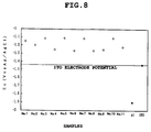
- Fig. 8 is a diagram showing electrode potential of a interconnector line of thin film of the invention in comparison with Al and ITO.
- a first interconnector line of thin film of the invention contains 0.001 to 30 at% of at least one type of first element constituting an intermetallic compound with Al and 0.01 atppm to 50 at% with respect to the amount of the first element of at least one type of second element selected from C, O, N and H, with the balance comprising substantially Al.
- the above-described first element can be various types of elements if they constitute an intermetallic compound with Al. Specifically, they can be rare earth metallic elements such as Y, Sc, La, Ce, Nd, Sm, Gd, Tb, Dy, Er, Gd and the like, Nb, Ta, Re, Mo, W, Zr, Hf and the like.
- intermetallic compound forming elements constituting the intermetallic compound with Al form, for example, an intermetallic compound such as Al 3 Y and function as a trap material for Al. Therefore, the diffusion of Al can be suppressed when thermal treatment is applied to an Al interconnector line of thin film or when the Al interconnector line of thin film is formed at a relatively high temperature. As a result, the occurrence of hillocks is prevented. And, electromigration and the like can also be suppressed.
- the intermetallic compound forming elements used are preferred to have a solid solubility of 1.0 wt% or below with respect to Al. If the solid solubility with respect to Al exceeds 1.0 wt%, a sufficient effect of suppressing hillocks owing to the constitution of an intermetallic compound with Al might not be attained, and specific resistance might increase.
- Such intermetallic compound forming elements are Ge, Li, Mg, Th, Ti, V, Zn, W and others.
- a second interconnector line of thin film of the invention contains 0.001 to 30 at% of at least one type of first element having a standard electrode potential higher than that of Al and 0.01 atppm to 50 at% with respect to the amount of the first element of at least one type of second element selected from C, O, N and H, with the balance comprising substantially Al.
- the above-described first element of the second interconnector line of thin film can be various types of elements if they have a standard electrode potential higher than that of Al. Specifically, they can be Ag, Au, Cu, Ti, V, Nb, Ta, Cr, Mo, W, Mn, Fe, Co, Ni, Pd, Ir, Pt, Cd, Si, Pb and the like. Among them, Ag, Au, Co, Cu, Mo, W and Mn having a standard electrode potential higher by 2V (298K) or more from that of Al are preferably used in particular.
- These elements (high electrode potential elements) having a higher standard electrode potential than Al can be contained in the Al interconnector line of thin film to raise a standard electrode potential of the Al interconnector line of thin film.
- the electrochemical reaction occurring between the Al interconnector line of thin film and the ITO electrode in an alkaline solution is a phenomenon which occurs owing to the movement of electrons because Al has a standard electrode potential lower than that of ITO. Therefore, by containing the high electrode potential elements into the Al interconnector line of thin film to increase the standard electrode potential of the Al interconnector line of thin film to exceed that of, for example, ITO, an electrochemical reaction between the Al interconnector line of thin film and the ITO electrode in the alkaline solution can be prevented.
- the gate line of, for example, LCD can be formed well with the Al interconnector line of thin film having a single layer structure without degrading the electrical characteristics due to coloring by reduction of the ITO electrode and oxidation of the Al interconnector line of thin film.
- Improvement of the standard electrode potential of the Al interconnector line of thin film by addition of the high electrode potential elements is effective not only when it is laminated with the ITO electrode but also when the Al interconnector line of thin film is laminated with an electrode, interconnector line and the like made of various types of materials having a standard electrode potential which is higher than that of Al.
- the above-described high electrode potential elements are preferably elements, which form an intermetallic compound with Al to suppress the specific resistance of the Al interconnector line of thin film from increasing. And, by using the elements constituting the intermetallic compound with Al as the high electrode potential element, the occurrence of hillocks and the electromigration can also be suppressed as described above. Thus, the elements, which have a standard electrode potential higher than that of Al and constitute an intermetallic compound with Al, are particularly effective.
- the Al interconnector line of thin film containing such elements can be used satisfactorily for either the signal line or the gate line of LCD and can be said having high general-purpose properties. Such elements are Pd, V, Ni, Mo, W and Co.
- the interconnector line of thin film of the invention comprises 0.001 to 50 at% of at least one type of the first element (element satisfying at least one of an intermetallic compound forming element and a high electrode potential element) selected from Y, Sc, La, Ce, Nd, Sm, Gd, Tb, Dy, Er, Th, Sr, Ti, Zr, V, Nb, Ta, Cr, Mo, W, Mn, Tc, Re, Fe, Co, Ni, Pd, Ir, Pt, Cu, Ag, Au, Cd, Si, Pb and B and 0.01 atppm to 50 at% with respect to the amount of the first element of at least one type of second element selected from C, O, N and H, with the balance comprising substantially Al.
- the first element element satisfying at least one of an intermetallic compound forming element and a high electrode potential element
- the first element selected from Y, Sc, La, Ce, Nd, Sm, Gd, Tb, Dy, Er, Th, Sr, Ti, Zr, V
- the above-described intermetallic compound forming element and high electrode potential element are contained in a range of 0.001 to 30 at% into the Al interconnector line of thin film.
- the intermetallic compound forming element is contained in an amount of less than 0.001 at%, the above-described hillock suppressing effect cannot be obtained satisfactorily.
- the intermetallic compound increases the resistance of the Al interconnector line of thin film and also becomes the cause of producing residues in dry etching or wet etching.
- the high electrode potential element is contained in an amount of less than 0.1 at%, the above-described electrochemical reaction suppressing effect cannot be obtained satisfactorily.
- the resistance of the Al interconnector line of thin film is increased, and residues are produced in dry etching or wet etching.
- a more preferable adding amount is in a range of 0.1 to 20 at%.
- the interconnector line of thin film of the invention has a very small amount of at least one type of element selected from C, O, N and H contained together with an element which satisfies at least either the intermetallic compound forming element or the high electrode potential element.
- This element (C, O, N, H) contained in a very small amount effectively acts on precipitation of a very small amount of the intermetallic compound, or the intermetallic compound forming element and the high electrode potential element itself. Therefore, the intermetallic compound, the intermetallic compound forming element and the high electrode potential element in the Al interconnector line of thin film can be precipitated finely and uniformly in the Al grains and grain boundaries.
- the etching property is improved extensively. Therefore, when the interconnector line network is formed on the Al interconnector line of thin film by dry etching or the like, the occurrence of etching residues can be suppressed substantially. And, as described in detail afterward, when the sputtering method is applied to produce the Al interconnector line of thin film of the present invention, at least one type of element selected from C, O, N and H is also effective to suppress the produced amount of dust by sputtering. Therefore, the Al interconnector line of thin film with the content of fine dust reduced substantially can be obtained.
- the first Al interconnector line of thin film of the invention excels in hillock resistance, does not cause an adverse effect on the subsequent process due to the occurrence of hillocks, and excels in forming a fine interconnector line network.
- an electrochemical reaction with the ITO electrode or the like in an alkaline solution is suppressed by containing therein the high electrode potential element.
- the second Al interconnector line of thin film of the invention excels in preventing the electrochemical reaction with the ITO electrode or the like and in forming the fine interconnector line network.
- the contained amount of at least one type of element (hereinafter referred to as fine precipitating element) selected from C, O, N and H as described above shall be in a range of 0.01 atppm to 50 at% with respect to an amount of the intermetallic compound forming element or the high electrode potential element in the Al interconnector line of thin film.
- fine precipitating element selected from C, O, N and H as described above.
- a more preferable contained amount of the fine precipitating element is in a range of 3 atppm to 3 at% when C is used, and 1.5 atppm to 7.5 at% when O, N and H are used.
- C is used as the fine precipitating element, it is more preferable that it is in a range of 300 to 3000 atppm with respect to the intermetallic compound forming element or the high electrode potential element, and desirably in a range of 600 to 1500 atppm.
- O, N and H are used as the fine precipitating element, it is more preferably in a range of 500 atppm to 1.5 at% with respect to the amount of the intermetallic compound forming element or the high electrode potential element, and desirably in a range of 300 to 1500 atppm.
- C is particularly effective for the fine precipitation of the intermetallic compound or the intermetallic compound forming element. Therefore, it is preferable to use C as the fine precipitating element for the first interconnector line of thin film.
- H acts on the fine precipitation of the intermetallic compound, the intermetallic compound forming element and the high electrode potential element and on additional improvement of the standard electrode potential of the Al interconnector line of thin film. Therefore, it is preferable to use H as the fine precipitating element for the second interconnector line of thin film. Namely, H lowers an ionization energy possessed by Al, the high electrode potential element and the intermetallic compound itself. Therefore, by using H as the fine precipitating element, the standard electrode potential of the Al interconnector line of thin film can be improved further. Otherwise, the contained amount of the high electrode potential element can be decreased.
- H promotes the chemical reaction in wet etching and acceleratingly promotes the reaction between an etching species (radical etc.) and the constituting elements of the Al interconnector line of thin film in dry etching, thereby contributing to improvement of the fine processing accuracy in etching.
- the contained amount of H in the Al interconnector line of thin film is preferably 500 wtppm or below.
- the first interconnector line of thin film of the invention can be obtained by, , forming the film by sputtering under general conditions, using for example the Al sputter target having the same composition therewith. And, the second interconnector line of thin film is also obtained in the same way.
- the sputter target used to form the first interconnector line of thin film comprises 0.001 to 30 at% of at least one type of intermetallic compound forming element constituting an intermetallic compound with Al and 0.01 atppm to 50 at% with respect to the intermetallic compound forming element of at least one type of fine precipitating element selected from C, O, N and H, with the balance comprising substantially Al.
- the sputter target used to form the second interconnector line of thin film comprises 0.001 to 30 at% of at least one type of high electrode potential element having a standard electrode potential higher than that of Al and 0.01 atppm to 50 at% with respect to the amount of the high electrode potential element of at least one type of fine precipitating element selected from C, O, N and H, with the balance comprising substantially Al.
- the sputter target of the invention can be a sputter target which comprises 0.001 to 30 at% of at least one type of first element (element satisfying at least either the intermetallic compound forming element or the high electrode potential element) selected from, for example, Y, Sc, La, Ce, Nd, Sm, Gd, Tb, Dy, Er, Th, Sr, Ti, Zr, V, Nb, Ta, Cr, Mo, W, Mn, Tc, Re, Fe, Co, Ni, Pd, Ir, Pt, Cu, Ag, Au, Cd, Si, Pb and B and 0.01 atppm to 50 at% of at least one type of second element (fine precipitating element) selected from C, O, N and H, with the balance comprising substantially Al.
- first element element satisfying at least either the intermetallic compound forming element or the high electrode potential element
- the interconnector line of thin film of the invention can be obtained with good reproducibility.
- the fine precipitating element also has an effect of suppressing the amount of dust produced by sputtering. Therefore, the Al interconnector line of thin film which is formed by sputtering using the sputter target of the invention has the contained amount of fine dust decreased substantially, excelling in forming the fine interconnector line network.
- At least one type of fine precipitating element selected from C, O, N and H can be taken into the Al interconnector line of thin film by controlling, for example, the sputtering atmosphere and conditions. But, it is desirable that it is previously contained into the sputter target to obtain an effect of suppressing the occurred amount of dust by sputtering.
- the above-described production method of the sputter target of the invention is not limited to a particular one, and it can be produced by applying a known production method such as atmosphere melting, vacuum melting, quench coagulation (e.g., spray foaming) or powder metallurgy.
- an element satisfying at least one of the intermetallic compound forming element and the high electrode potential element and the fine precipitating element such as C are mixed in a predetermined amount with Al, and undergone high-frequency melting in vacuum to produce an ingot.
- O, N and H are used as the fine precipitating element, taking into consideration the contained amount as the impurity element, and such gas is bubbled while melting to contain in a given amount into the ingot.
- O, N and H are used as the fine precipitating element, it is preferable to adopt the vacuum melting in order to control their contained amount.
- an element satisfying at least either the intermetallic compound forming element or the high electrode potential element and the fine precipitating element are mixed with Al in a given amount in the same way, undergone high-frequency melting, and sprayed by a spray to produce an ingot.
- O, N and H are used as the fine precipitating element, taking into account the contained amount as the impurity element, such gas is injected when spraying to contain in a given amount into the ingot.
- the fine precipitating element and an element satisfying at least either the intermetallic compounding forming element or the high electrode potential element are mixed in a given amount with Al, and subjected to atmosphere sintering, hot press, HIP or the like to produce a sinter.
- atmosphere sintering, hot press, HIP or the like to produce a sinter.
- O, N and H are used as the fine precipitating element, N can be contained from N 2 atmosphere when the sinter is produced.
- an amount contained in Al mother material is specified.
- O, N and H are contained in a predetermined amount into the sinter.
- the quench coagulation by which a high-purity and fine-crystalline material with a relatively high density can be obtained easily, is suitable.
- Hot processing or cold processing is generally applied to the ingot obtained by melting and the sinter obtained by powder metallurgy. And, if necessary, recrystallization heat processing and crystal orientation controlling are performed to obtain a desired sputter target.
- recrystallization heat processing and crystal orientation controlling are performed to obtain a desired sputter target.
- diffusion bonding or the like may be performed to obtain a target having a desired shape. But, when a large target which is used to form a large area LCD or the like is produced, it is preferable to form collectively by various types of methods in view of suppressing the occurrence of dust by sputtering.
- the sputter target of the invention when the sputter target of the invention is produced, it is preferable to have a processing rate of 50% or more by rolling, forging or the like. This is because the heat energy obtained from the above-described processing rate is effective to produce an array of conformed crystal lattices and to decrease fine internal defects. Since the required purity, composition, plane direction and the like are different depending on the desired sputter target, the production method can be determined appropriately according to the required properties.
- the production method for the Al interconnector line of thin film of the invention is not limited to the above-described sputtering and can be various types of film forming methods if an Al interconnector line of thin film satisfying the above-described composition can be applied.
- the Al interconnector line of thin film of the invention is not limited to the sputter film but can be thin films produced by various types of film forming methods if they are the Al interconnector line of thin films satisfying the above-described composition.
- the above-described Al interconnector line of thin film of the invention can be used for interconnector line, electrode and the like of various types of electronic parts. Specifically, they are a liquid crystal display (LCD) using the Al interconnector line of thin film of the invention as the gate line, signal line and the like, and semiconductor devices such as VLSI, ULSI and the like using the Al interconnector line of thin film of the invention as the interconnector line network.
- the Al interconnector line of thin film of the invention can also be used for a surface acoustic wave oscillator (SAW) and interconnector line of electronic parts such as an SAW device using the SAW, and a thermal printer head (TPH).
- SAW surface acoustic wave oscillator
- TPH thermal printer head
- the electronic parts of the invention are particularly effective for an enlarged and high-resolution LCD panel and a highly integrated semiconductor device.
- Fig. 1 and Fig. 2 are diagrams showing one embodiment of a liquid crystal display using the Al interconnector line of thin film of the invention.
- Fig. 1 is an equivalent circuit diagram of an active matrix liquid crystal display using a reverse staggered structure TFT
- Fig. 2 is a sectional view showing the structure of the pertinent TFT.
- Fig. 1 denotes a transparent glass substrate on which gate interconnector line 2 and data interconnector line 3 are disposed into the form of a matrix
- a TFT 4 is formed by a-Si film at respective crossings of interconnector line.
- the sectional structure of the TFT 4 has a gate electrode 2' made of the Al interconnector line of thin film (Al alloy film) of the invention formed on the transparent glass substrate 1.
- This gate electrode 2' is integrally formed by the same material and the same process as the gate electrode 2 of Fig. 1.
- an Si 3 N 4 film 5 is formed as a gate insulating film thereon, a non-dope a-Si film 6 and an n + type a-Si film 7 are formed thereon, and an Mo film 8 is formed thereon.
- a drain electrode 3' and a source electrode 9 are formed thereon.
- a surface electrode 10 and a liquid crystal capacitance 11 of each pixel are connected to the source of the TFT 4.
- Fig. 3 is a sectional view showing the main structure of one embodiment of a semiconductor device using the Al interconnector line of thin film of the invention. The structure of this semiconductor device will be described together with its production process.
- 21 is a p-Si substrate, and heat oxidation is applied to this p-Si substrate to form a heat-oxidized film on the surface. Then, oxidation treatment is performed selectively excepting each region of source, gate and drain to form a field oxidized film 22. Then, the heat-oxidized film on the respective source and drain regions is removed by the formation of the resist film and etching treatment (PEP treatment). By this PEP treatment, a gate-oxidized film 23 is formed. Then, a resist film is formed excluding the respective source and drain regions, and impurity elements are implanted into the p-Si substrate 21 to form a source region 24 and a drain region 25. And, a silicide film 26 of Mo or W is formed on the gate-oxidized film 23.
- PEP treatment etching treatment
- the phosphorus silicate glass layer 27 on the source region 24 and the drain region 25 is removed by PEP treatment.
- a barrier layer 28 of TiN, ZrN, HfN or the like is formed on the source region 24 and the drain region 25 from which the phosphorus silicate glass layer 27 was removed.
- the Al interconnector line of thin film (Al alloy film) of the invention is formed on the entire surface, and the PEP treatment is applied to form Al interconnector line 29 having a desired shape. And, after forming an insulation film 30 made of an Si 3 N 4 film or the like, an opening for bonding an Au lead 31 is formed by the PEP treatment to complete a semiconductor chip 32.
- Fig. 4 is an exploded perspective view showing the structure of main parts of one embodiment of a thermal printer head using the Al interconnector line of thin film of the invention.
- a heat-resistant resin layer 32 made of an aromatic polyimide resin or the like is formed on a supporting substrate 31 made of, for example, an Fe-Cr alloy.
- a base film 33 mainly consisting of, for example, Si and one of N or C is formed on the heat-resistant resin 32 by sputtering or the like.
- An exothermic resistor 34 and respective electrodes 35 and common electrodes 36 made of the Al interconnector line of thin film of the invention are formed on the base film 33.
- a protective film 37 is formed to cover most of the electrodes 35, 36 and the exothermic resistor 34.
- Fig. 5, Fig. 6 and Fig. 7 are diagrams showing an SAW and an SAW device using the Al interconnector line of thin film of the invention.
- Fig. 5 is a plan view showing the structure of an SAW according to one embodiment
- Fig. 6 is a plan view showing the structure of an SAW according to another embodiment
- Fig. 7 is a sectional view showing the structure of an SAW device using the SAW.
- transducers 42, 43 made of the Al interconnector line of thin film of the invention are formed separately on a piezoelectric substrate 41 made of an LiTaO 3 substrate and an LiNbO 3 substrate. Weighting is performed to change a crossing width of the electrodes of the transducer, e.g., the input transducer 42, to make a filter, e.g., a PIF filter of a color TV receiver. A non-crossed part of the weighted input transducer 42 is fully covered with the Al alloy film of the invention to make large an electrode terminal 44 of the input transducer 42.
- a sound absorbing material 45 is disposed in an overlaid form on at least a part of the electrode terminal 44 formed in this way and the outer part of the input transducer 42.
- the shape of the sound absorbing material 45 is made to have a slanted side edge so to cover most of the rear edge of the input transducer 42 and to cross slantingly with a surface acoustic wave where the incident side of the surface acoustic wave enters.
- a sound absorbing material 46 is also disposed on the outer side of the output transducer 43.
- Fig. 6 is a plan view showing the SAW according to another embodiment.
- a transducer for transforming an input electric signal into a surface acoustic wave propagating on the piezoelectric substrate 41 for example, an interdigital electrode 47 made of a pair of comb-teeth type electrodes 47a and 47b mutually engaged, is formed on a piezoelectric substrate 41 consisting of an LiTaO 3 substrate or an LiNbO 3 substrate.
- This interdigital electrode 47 is made of the Al alloy film of the invention.
- Grading reflectors 48, 49 which is to reflect the surface acoustic wave excited by the interdigital electrode 47, and is made of the Al alloy film of the invention are formed on the piezoelectric substrate 41 at both ends of the interdigital electrode 47.
- the SAW shown in Fig. 5 and Fig. 6 is used as a device shown in Fig. 7.
- an SAW 51 is fixed onto a chip carrier 53 made of, for example, a ceramics substrate, through an adhesive member 52, and a metallic cap 55 is put on the chip carrier 53 through a ring 54 made of a low-thermal expansion metal such as Kovar.
- a interconnector line pattern 56 made of the Al alloy film of the invention is formed on the chip carrier 53.
- the SAW 51 and the interconnector line pattern 56 are electrically connected by a bonding wire 57.
- the interconnector line pattern 56 (each independent pattern) on the chip carrier 53 is electrically connected to an interconnector line pattern 59 on the bottom side of the chip carrier 53 via a through hole 58 having gold or the like applied on its inner wall and sealed by an insulating material such as glass.
- an Al film having a thickness of 350nm was formed by spin precipitation on a glass substrate having a diameter of 5 inches under conditions of a back pressure of 1x10 -4 Pa, power of 200W DC and sputter time of 3 min.
- the Al film was measured to evaluate on a specific resistance, a hillock density after the heat treatment (573 K) and the presence or not of etching residue.
- Etching for an evaluation test of the etching residue was performed using a BCl 3 + Cl 2 mixture gas as etching gas. The results are shown in Table 1.
- an Al sputter target (comparative example 1-1) produced without adding Y and C and an Al sputter target (comparative example 1-2) produced under the same conditions as Example 1 excepting that C was not added were used to form Al films in the same way by sputtering. And, these Al films were also evaluated for properties in the same way as in Example 1. These results (after the heat treatment) are also shown in Table 1.
- Target composition Evaluated properties of Al sputter film Amount of intermetallic compound forming elements Amount of C Specific resistance ( ⁇ ⁇ cm) Hillock density after heat treatment Etching residue Example 1 A1-0.83at%Y 1630at. ppm 3.14 ⁇ Non Comparative example 1-1 Al Non 3.00 X Non Comparative example 1-2 A1-0.83at%Y Non 3.01 o ⁇ Yes
- the Al interconnector line of thin film of the invention excels in hillock resistance and etching.
- a good fine interconnector line network can be formed with good reproducibility.
- Example 2 After producing the Al sputter targets having respective compositions shown in Table 2 in the same way as in Example 1, sputtering was performed under the same conditions as in Example 1 to produce respective Al interconnector line of thin films. These Al interconnector line of thin films were measured to evaluate their properties in the same way as in Example 1. The results are also shown in Table 2.
- Al interconnector line of thin films were measured to evaluate their properties in the same way as in Example 1. And, the Al interconnector line of thin films of sample Nos. 16 through 21 were measured to evaluate reactivity with the ITO electrode in an alkaline solution. Reactivity with the ITO electrode in the alkaline solution was examined by a generally used electrode measuring method using silver/silver chloride electrodes as a reference electrode and ITO as the anode and respective Al alloys as the cathode. The results are also shown in Table 3.
- material having 2.84 at% (6 wt%) of Co added to Al was undergone high-frequency melting (vacuum melting), and H 2 gas was bubbled into the melted metal to give H therein.
- the bubbling amount of H was set so that the amount of H in an ingot becomes 980 atppm (200 wtppm) with respect to the amount of Co.
- the ingot thus produced to have a target composition was undergone hot rolling and machining to obtain an Al sputter target having a diameter of 127 mm and a thickness of 5 mm.
- an Al film having a thickness of 350nm was formed by spin precipitation on a glass substrate having a diameter of 5 inches under conditions of a back pressure of 1x10 -4 Pa, power of 200W DC and sputter time of 2 min.
- the Al film was undergone patterning and dry etching and measured to evaluate on a specific resistance, a hillock density and the presence or not of etching residue after the heat treatment at 573 K. The results are shown in Table 4.
- the evaluation test of the etching residue was performed using a BCl 3 + Cl 2 mixture gas as etching gas.
- Target composition Evaluated properties of Al sputter film Amount of added elements (atomic ratio) Amount of H (atomic ratio) Specific resistance ( ⁇ ⁇ cm) Hillock density after heat treatment Etching residue
- Example 4 Al-2.84%Co 980ppm 4.3 o ⁇ Non Comparative example 4-1 Al Non 2.9 X Non Comparative example 4-2 Al-2.84%Co Non 4.2 ⁇ Yes
- the Al interconnector line of thin film of example 4 excels in hillock resistance and etching. Therefore, by using this Al interconnector line of thin film, a good fine interconnector line network can be formed with good reproducibility.
- the Al film containing an element having a standard electrode potential higher than Al has an electrode potential higher than that of the ITO.
- the Al sputter targets having the compositions shown in Table 6 were produced in the same way as in Example 4, and films were formed by sputtering under the same conditions as in Example 4 to obtain the Al interconnector line of thin films. These Al interconnector line of thin films were measured to evaluate their reactivity with the ITO electrode in an alkaline solution. The results are also shown in Table 6. Comparative example 6 in Table 6 has the contained amount of high electrode potential elements fell outside the range of the invention.
- the respective Al interconnector line of thin films having an appropriate amount of high electrode potential elements and H contained according to Example 6 excelling in specific resistance, hillock resistance, etching and resistance of reaction with the ITO electrode. Therefore, by using such an Al interconnector line of thin film, a good fine interconnector line network can be formed with good reproducibility. And, the gate line or the like of the LCD can also be formed properly.
- the Al sputter targets having the compositions shown in Table 7 were produced in the same way as in Example 4, and films were formed by sputtering under the same conditions as in Example 4 to obtain the Al interconnector line of thin films. These Al interconnector line of thin films were measured to evaluate their properties in the same way as in Example 1. And, the etching property of the Al interconnector line of thin films was examined on the etching rate of wet etching and dry etching respectively. The results are shown in Table 7.
- Comparative example 7 in Table 7 shows Al films formed by sputtering in the same way respectively using the Al sputter target produced in the same conditions as Example 7 excepting that H was not added.
- each Al interconnector line of thin film according to Example 7 containing an appropriate amount of high electrode potential element and H excels in specific resistance and anti-hillock property and also has high etching rate property. Therefore, by using this Al interconnector line of thin film, a good fine interconnector line network can be formed with good reproducibility and high efficiency.
- material having 0.3 at% (2 wt%) of Ta added to Al was undergone high frequency melting (vacuum melting), and O 2 was bubbled to enter oxygen when melting.
- the entered amount of oxygen was set so that the amount of O in an ingot becomes 10 atppm (300 wtppm) with respect to the amount of Ta.
- the ingot thus produced to have a target composition was undergone hot rolling and machining to obtain an Al sputter target having a diameter of 127 mm and a thickness of 5 mm.
- an Al film having a thickness of 350nm was formed by spin precipitation on a glass substrate having a diameter of 5 inches under conditions of a back pressure of 1x10 -4 Pa, power of 200W DC and sputter time of 2 min.
- the Al film was undergone patterning and dry etching and measured to evaluate on a specific resistance, a hillock density and the presence or not of etching residue after the heat treatment at 573 K.
- the results are shown in Table 9.
- the evaluation test of the etching residue was performed using a BCl3 + Cl2 mixture gas as etching gas.
- an Al sputter target (comparative example 9-1) produced with no addition of Ta and O and an Al sputter target (comparative example 9-2) produced under the same conditions excepting no addition of O as in Example 9 were used to form an Al film in the same way by sputtering. And, these Al films were also evaluated on their properties in the same way as in Example 9. These results are also shown in Table 9.
- Target composition Evaluated sputter properties film of Al Added amount of elements Amount of O Specific resistance ( ⁇ ⁇ cm) Hillock density after heat treatment Etching residue
- Example 9 Al-0.3at%Ta 10ppm 3.3 o ⁇
- Non Comparative example 9-1 Al Non 3.1 X
- Non Comparative example 9-2 Al-0.3at%Ta Non 3.2 o ⁇ Yes
- the Al interconnector line of thin film of Example 9 excels in anti-hillock property and etching property. Therefore, by using this Al interconnector line of thin film, a good fine interconnector line network can be formed with good reproducibility.
- Al targets compositions shown in Table 10 using various types of elements were produced in the same way as in Example 9, films were formed by sputtering under the same conditions as in Example 9 to obtain respective Al interconnector line of thin films.
- material having 0.28at% (2wt%) of Pt added to Al underwent high-frequency melting (vacuum melting) and N 2 was bubbled to enter nitrogen while melting.
- the entered amount of nitrogen was determined so that the amount of N in an ingot becomes 19atppm (500wtppm) against the amount of Pt.
- the ingot produced to have the target composition was undergone hot rolling and machining to obtain an Al sputter target having a diameter of 127 mm and a thickness of 5 mm.
- an Al film having a thickness of 350nm was formed by spin precipitation on a glass substrate having a diameter of 5 inches under conditions of a back pressure of 1x10 -4 Pa, power of 200W DC and sputter time of 2 min.
- the Al film was undergone patterning and dry etching and measured to evaluate on a specific resistance, a hillock density and the presence or not of etching residue after the heat treatment at 573 K. The results are shown in Table 11.
- the evaluation test of the etching residue was performed using a BCl 3 + Cl 2 mixture gas as etching gas.
- an Al sputter target (Comparative example 11-1) produced with no addition of Pt and N and an Al sputter target (Comparative example 11-2) produced under the same conditions as in Example 11 excepting that N was not added were used to form Al films by sputtering in the same way. And, these Al films were also evaluated on their properties in the same way as in Example 11. These results are also shown in Table 11.
- Target composition Evaluated properties of Al sputter film Added amount of elements Amount of N Specific resistance ( ⁇ ⁇ cm) Hillock density after heat treatment Etching residue
- Example 11 Al-0.28at% 19ppm 3.4 o ⁇ Non Comparative example 11-1 Al Non 3.1 X Non Comparative example 11-2 Al-0.28at% Non 3.2 ⁇ Yes
- the Al interconnector line of thin film of Example 11 excels in anti-hillock property and etching property. Therefore, by using this Al interconnector line of thin film, a good fine interconnector line network can be formed with good reproducibility.
- the interconnector line of thin film of the invention has low resistance and also excels in anti-hillock property, etching property, preventing property of an electrochemical reaction with ITO or the like. Therefore, by using the interconnector line of thin film of the invention, LCD's signal lines, gate lines, and very fine interconnector line network of a semiconductor device can be formed well. And, with the sputter target of the invention, the above-described low resistance interconnector line of thin film can be formed with good reproducibility, and the occurrence of dust in sputtering can be suppressed.
Landscapes
- Chemical & Material Sciences (AREA)
- Engineering & Computer Science (AREA)
- Materials Engineering (AREA)
- Mechanical Engineering (AREA)
- Metallurgy (AREA)
- Organic Chemistry (AREA)
- Chemical Kinetics & Catalysis (AREA)
- Acoustics & Sound (AREA)
- Physics & Mathematics (AREA)
- Physical Vapour Deposition (AREA)
- Electrodes Of Semiconductors (AREA)
- Internal Circuitry In Semiconductor Integrated Circuit Devices (AREA)
- Powder Metallurgy (AREA)
- Thin Film Transistor (AREA)
- Insulated Gate Type Field-Effect Transistor (AREA)
- Liquid Crystal (AREA)
Priority Applications (1)
| Application Number | Priority Date | Filing Date | Title |
|---|---|---|---|
| EP05003598.9A EP1553205B1 (de) | 1995-10-12 | 1996-10-14 | Sputtertarget zur Dünnschicht-Leitungherstellung und Dünnschicht-Leitung |
Applications Claiming Priority (3)
| Application Number | Priority Date | Filing Date | Title |
|---|---|---|---|
| JP264472/95 | 1995-10-12 | ||
| JP26447295 | 1995-10-12 | ||
| PCT/JP1996/002961 WO1997013885A1 (fr) | 1995-10-12 | 1996-10-14 | Film de cablage, cible de pulverisation par bombardement ionique destinee a la formation de ce film et composant electronique comportant ce film |
Related Child Applications (1)
| Application Number | Title | Priority Date | Filing Date |
|---|---|---|---|
| EP05003598.9A Division EP1553205B1 (de) | 1995-10-12 | 1996-10-14 | Sputtertarget zur Dünnschicht-Leitungherstellung und Dünnschicht-Leitung |
Publications (2)
| Publication Number | Publication Date |
|---|---|
| EP0855451A1 true EP0855451A1 (de) | 1998-07-29 |
| EP0855451A4 EP0855451A4 (de) | 1999-10-06 |
Family
ID=17403704
Family Applications (2)
| Application Number | Title | Priority Date | Filing Date |
|---|---|---|---|
| EP05003598.9A Expired - Lifetime EP1553205B1 (de) | 1995-10-12 | 1996-10-14 | Sputtertarget zur Dünnschicht-Leitungherstellung und Dünnschicht-Leitung |
| EP96933629A Withdrawn EP0855451A4 (de) | 1995-10-12 | 1996-10-14 | Drahtfilm, sputtertarget zur herstellung des drahtfilms und elektronische teile, die diesen verwenden |
Family Applications Before (1)
| Application Number | Title | Priority Date | Filing Date |
|---|---|---|---|
| EP05003598.9A Expired - Lifetime EP1553205B1 (de) | 1995-10-12 | 1996-10-14 | Sputtertarget zur Dünnschicht-Leitungherstellung und Dünnschicht-Leitung |
Country Status (6)
| Country | Link |
|---|---|
| US (2) | US6329275B1 (de) |
| EP (2) | EP1553205B1 (de) |
| JP (7) | JP4137182B2 (de) |
| KR (1) | KR100312548B1 (de) |
| TW (1) | TW318276B (de) |
| WO (1) | WO1997013885A1 (de) |
Cited By (18)
| Publication number | Priority date | Publication date | Assignee | Title |
|---|---|---|---|---|
| EP0998592A4 (de) * | 1997-07-15 | 2001-02-28 | Micron Technology Inc | Verfahren zur benutzung von wasserstoff- und sauerstoffgas in sputterabscheidung von aluminiumhaltigen filmen und danach hergestellte aluminiumhaltige filme |
| WO2001029866A1 (en) * | 1999-10-19 | 2001-04-26 | Candescent Intellectual Property Services, Inc. | Electrode structure and related method |
| US6448708B1 (en) | 1997-09-17 | 2002-09-10 | Candescent Intellectual Property Services, Inc. | Dual-layer metal for flat panel display |
| US6455939B1 (en) | 1997-07-15 | 2002-09-24 | Micron Technology, Inc. | Substantially hillock-free aluminum-containing components |
| WO2003029510A1 (fr) * | 2001-09-18 | 2003-04-10 | Mitsui Mining & Smelting Co.,Ltd. | Film mince d'alliage d'aluminium, circuit de connexions comportant ce film et materiau cible pour former ledit film |
| US6736947B1 (en) * | 1997-12-24 | 2004-05-18 | Kabushiki Kaisha Toshiba | Sputtering target, A1 interconnection film, and electronic component |
| SG118219A1 (en) * | 2002-12-19 | 2006-01-27 | Kobe Steel Ltd | Electronic device method of manufacture of the same and sputtering target |
| EP1642996A2 (de) | 2004-09-30 | 2006-04-05 | Kabushiki Kaisha Kobe Seiko sho | Verschleissfeste und oxidationbeständige Hartbeschichtung und Target zur Herstellung |
| EP1698714A3 (de) * | 2000-12-28 | 2006-09-27 | Kabushiki Kaisha Kobe Seiko Sho | Target zur Bildung einer Hartschicht |
| US7161211B2 (en) | 1997-07-15 | 2007-01-09 | Micron Technology, Inc. | Aluminum-containing film derived from using hydrogen and oxygen gas in sputter deposition |
| EP1878809A4 (de) * | 2005-04-26 | 2008-07-09 | Mitsui Mining & Smelting Co | Verdrahtungsmaterial aus al-ni-b-legierung und elementstruktur damit |
| USRE41975E1 (en) | 1995-10-12 | 2010-11-30 | Kabushiki Kaisha Toshiba | Interconnector line of thin film, sputter target for forming the wiring film and electronic component using the same |
| US8492862B2 (en) | 2009-11-13 | 2013-07-23 | Semiconductor Energy Laboratory Co., Ltd. | Sputtering target and manufacturing method thereof, and transistor |
| US8558248B2 (en) | 2007-09-19 | 2013-10-15 | Mitsubishi Electric Corporation | A1 alloy film, electronic device, and active matrix substrate for use in electrooptic display device |
| USRE45481E1 (en) | 1995-10-12 | 2015-04-21 | Kabushiki Kaisha Toshiba | Interconnector line of thin film, sputter target for forming the wiring film and electronic component using the same |
| CN108431301A (zh) * | 2015-12-23 | 2018-08-21 | 埃托特克德国有限公司 | 铜和铜合金表面用蚀刻溶液 |
| US10332996B2 (en) | 2009-12-04 | 2019-06-25 | Semiconductor Energy Laboratory Co., Ltd. | Semiconductor device and manufacturing method thereof |
| US11236416B2 (en) | 2016-06-07 | 2022-02-01 | Jx Nippon Mining & Metals Corporation | Sputtering target and production method therefor |
Families Citing this family (71)
| Publication number | Priority date | Publication date | Assignee | Title |
|---|---|---|---|---|
| JPH10142625A (ja) * | 1996-11-07 | 1998-05-29 | Vacuum Metallurgical Co Ltd | 液晶ディスプレイの導電部製作方法及びその製作に用いるスパッタリングターゲット |
| JP2002373867A (ja) * | 2001-06-14 | 2002-12-26 | Idemitsu Kosan Co Ltd | 半導体素子用導電性薄膜、半導体素子及びそれらの製造方法 |
| CN1643683A (zh) * | 2002-01-24 | 2005-07-20 | 霍尼韦尔国际公司 | 薄膜、具有薄膜的结构以及形成薄膜的方法 |
| JP2004143584A (ja) * | 2002-08-29 | 2004-05-20 | Nippon Sheet Glass Co Ltd | ジルコニウム化合物膜が被覆された物品、その物品の製造方法及びその膜を被覆するために用いるスパッタリングターゲット |
| EP1411146B1 (de) * | 2002-10-17 | 2010-06-09 | Samsung Electronics Co., Ltd. | Verfahren zur Herstellung eines Kobaltsilizidfilms und zur Herstellung einer einen Kobaltsilizidfilm enthaltenden Halbleitervorrichtung |
| JP2006339666A (ja) * | 2002-12-19 | 2006-12-14 | Kobe Steel Ltd | アルミニウム合金膜形成用スパッタリングターゲット |
| CN1307694C (zh) * | 2003-06-03 | 2007-03-28 | 旺宏电子股份有限公司 | 降低半导体组件中二硅化钴层的电阻值的方法 |
| US7030430B2 (en) * | 2003-08-15 | 2006-04-18 | Intel Corporation | Transition metal alloys for use as a gate electrode and devices incorporating these alloys |
| JP2005086118A (ja) * | 2003-09-11 | 2005-03-31 | Renesas Technology Corp | 半導体装置 |
| US20070102822A1 (en) * | 2003-12-18 | 2007-05-10 | Takashi Kubota | Aluminum base target and process for producing the same |
| EP1998355A3 (de) * | 2004-01-22 | 2009-02-25 | Canon Kabushiki Kaisha | Antistatische Folie, Distanzstück damit und Bildanzeigeeinheit |
| CN103121799A (zh) * | 2004-03-09 | 2013-05-29 | 出光兴产株式会社 | 溅射靶、透明导电膜、薄膜晶体管、薄膜晶体管基板及其制造方法及液晶显示装置 |
| CN100417993C (zh) * | 2004-03-25 | 2008-09-10 | 三井金属鉱业株式会社 | 薄膜电路的接合结构 |
| TWI298351B (en) * | 2004-03-25 | 2008-07-01 | Mitsui Mining & Smelting Co | Bonded structure for a thin-film circuit |
| JP4849821B2 (ja) * | 2004-04-28 | 2012-01-11 | 株式会社半導体エネルギー研究所 | 表示装置、電子機器 |
| US7550769B2 (en) * | 2004-06-11 | 2009-06-23 | Semiconductor Energy Laboratory Co., Ltd. | Light emitting element, light emitting device and semiconductor device |
| WO2006057312A1 (ja) * | 2004-11-24 | 2006-06-01 | Tosoh Corporation | 配線・電極及びスパッタリングターゲット |
| WO2006117884A1 (ja) * | 2005-04-26 | 2006-11-09 | Mitsui Mining & Smelting Co., Ltd. | Al-Ni-B合金配線材料及びそれを用いた素子構造 |
| US20070017803A1 (en) * | 2005-07-22 | 2007-01-25 | Heraeus, Inc. | Enhanced sputter target manufacturing method |
| EP1923480A3 (de) * | 2005-07-22 | 2008-06-18 | Heraeus, Inc. | Verbessertes Herstellungsverfahren für Sputtertargets |
| JP4117002B2 (ja) | 2005-12-02 | 2008-07-09 | 株式会社神戸製鋼所 | 薄膜トランジスタ基板および表示デバイス |
| JP2007191761A (ja) * | 2006-01-19 | 2007-08-02 | Idemitsu Kosan Co Ltd | 積層構造、それを用いた電気回路用電極及びその製造方法 |
| WO2007102988A2 (en) * | 2006-03-06 | 2007-09-13 | Tosoh Smd, Inc. | Electronic device, method of manufacture of same and sputtering target |
| US20090008786A1 (en) | 2006-03-06 | 2009-01-08 | Tosoh Smd, Inc. | Sputtering Target |
| JP4728170B2 (ja) | 2006-05-26 | 2011-07-20 | 三菱電機株式会社 | 半導体デバイスおよびアクティブマトリクス型表示装置 |
| JP5234892B2 (ja) * | 2006-05-31 | 2013-07-10 | 株式会社神戸製鋼所 | 薄膜トランジスタ基板および表示デバイス |
| CN101365816B (zh) * | 2006-10-16 | 2010-10-06 | 三井金属鉱业株式会社 | 反射膜用Al-Ni-B合金材料 |
| WO2008050710A1 (fr) * | 2006-10-26 | 2008-05-02 | Mitsui Mining & Smelting Co., Ltd. | MATÉRIAU DE CÂBLAGE D'ALLIAGE À BASE D'Al ET STRUCTURE D'ÉLÉMENT L'UTILISANT |
| JP4377906B2 (ja) * | 2006-11-20 | 2009-12-02 | 株式会社コベルコ科研 | Al−Ni−La系Al基合金スパッタリングターゲット、およびその製造方法 |
| JP4170367B2 (ja) | 2006-11-30 | 2008-10-22 | 株式会社神戸製鋼所 | 表示デバイス用Al合金膜、表示デバイス、及びスパッタリングターゲット |
| WO2008066030A1 (fr) * | 2006-11-30 | 2008-06-05 | Kabushiki Kaisha Kobe Seiko Sho | Film d'alliage d'al pour un dispositf d'affichage, dispositf d'affichage, et cible de pulvérisation cathodique |
| KR100818525B1 (ko) * | 2006-12-20 | 2008-03-31 | 동부일렉트로닉스 주식회사 | 이미지 센서 및 그의 제조방법 |
| KR100853545B1 (ko) | 2007-05-15 | 2008-08-21 | 삼성에스디아이 주식회사 | 유기전계발광소자 및 그의 제조방법 |
| JP2009010052A (ja) * | 2007-06-26 | 2009-01-15 | Kobe Steel Ltd | 表示装置の製造方法 |
| JP2009008770A (ja) | 2007-06-26 | 2009-01-15 | Kobe Steel Ltd | 積層構造およびその製造方法 |
| JP5143649B2 (ja) * | 2007-07-24 | 2013-02-13 | 株式会社コベルコ科研 | Al−Ni−La−Si系Al合金スパッタリングターゲットおよびその製造方法 |
| RU2354729C1 (ru) * | 2007-10-02 | 2009-05-10 | Юлия Алексеевна Щепочкина | Спеченный сплав |
| WO2009123217A1 (ja) * | 2008-03-31 | 2009-10-08 | 株式会社神戸製鋼所 | 表示装置、その製造方法およびスパッタリングターゲット |
| JP5308760B2 (ja) * | 2008-09-30 | 2013-10-09 | 株式会社日立製作所 | 表示装置 |
| KR20120048590A (ko) * | 2009-07-31 | 2012-05-15 | 고쿠리츠 다이가쿠 호진 도호쿠 다이가쿠 | 반도체 장치, 반도체 장치의 제조 방법, 및 표시 장치 |
| KR20170076818A (ko) * | 2009-11-13 | 2017-07-04 | 가부시키가이샤 한도오따이 에네루기 켄큐쇼 | 스퍼터링 타겟 및 그 제작 방법 및 트랜지스터 |
| TW201140627A (en) * | 2010-05-05 | 2011-11-16 | Univ Nat Yunlin Sci & Tech | Method for producing aluminum foil electrode of carbon nano-tube |
| JP5032687B2 (ja) * | 2010-09-30 | 2012-09-26 | 株式会社神戸製鋼所 | Al合金膜、Al合金膜を有する配線構造、およびAl合金膜の製造に用いられるスパッタリングターゲット |
| US8894825B2 (en) | 2010-12-17 | 2014-11-25 | Semiconductor Energy Laboratory Co., Ltd. | Sputtering target, method for manufacturing the same, manufacturing semiconductor device |
| JP5909852B2 (ja) * | 2011-02-23 | 2016-04-27 | ソニー株式会社 | 半導体装置の製造方法 |
| JP2012186199A (ja) * | 2011-03-03 | 2012-09-27 | Toshiba Corp | 半導体発光装置およびその製造方法 |
| JP6461543B2 (ja) * | 2013-10-08 | 2019-01-30 | 株式会社フルヤ金属 | アルミニウムと希土類元素との合金ターゲット及びその製造方法 |
| CN103952604B (zh) * | 2014-04-10 | 2016-06-08 | 安徽银力铸造有限公司 | 一种汽车用防锈铝合金 |
| CN104451281A (zh) * | 2014-12-25 | 2015-03-25 | 春焱电子科技(苏州)有限公司 | 一种电子材料用铝合金 |
| US10494712B2 (en) * | 2015-05-21 | 2019-12-03 | Jx Nippon Mining & Metals Corporation | Copper alloy sputtering target and method for manufacturing same |
| JP6574714B2 (ja) * | 2016-01-25 | 2019-09-11 | 株式会社コベルコ科研 | 配線構造およびスパッタリングターゲット |
| CN105586576A (zh) * | 2016-02-04 | 2016-05-18 | 东莞沙头朝日五金电子制品有限公司 | 一种镀制pvd防菌膜的方法 |
| CN106521250B (zh) * | 2016-12-05 | 2018-03-20 | 合肥工业大学 | 一种大载流耐热铝合金导线的制备方法 |
| CN106555083B (zh) * | 2016-12-05 | 2018-03-20 | 合肥工业大学 | 一种全铝合金架空导线及其制备方法 |
| WO2018169998A1 (en) * | 2017-03-13 | 2018-09-20 | Materion Corporation | Aluminum-scandium alloys with high uniformity and elemental content and articles thereof |
| US10760156B2 (en) | 2017-10-13 | 2020-09-01 | Honeywell International Inc. | Copper manganese sputtering target |
| US11035036B2 (en) | 2018-02-01 | 2021-06-15 | Honeywell International Inc. | Method of forming copper alloy sputtering targets with refined shape and microstructure |
| CN108396205B (zh) * | 2018-04-28 | 2020-09-04 | 广州致远新材料科技有限公司 | 一种铝合金材料及其制备方法 |
| WO2020003667A1 (ja) * | 2018-06-28 | 2020-01-02 | 株式会社アルバック | アルミニウム合金膜、その製造方法、及び薄膜トランジスタ |
| JP6735930B2 (ja) * | 2018-06-28 | 2020-08-05 | 株式会社アルバック | アルミニウム合金ターゲット及びその製造方法 |
| JP7096291B2 (ja) * | 2019-11-26 | 2022-07-05 | 株式会社フルヤ金属 | スパッタリングターゲット |
| KR102789960B1 (ko) * | 2019-07-31 | 2025-04-03 | 가부시키가이샤 후루야긴조쿠 | 스퍼터링 타겟 |
| CN110923529A (zh) * | 2019-11-29 | 2020-03-27 | 安徽峰创云通数据科技有限公司 | 电力电缆用Al-Cu-Sr-RE-Ge铝合金线及其制备方法 |
| KR102329427B1 (ko) * | 2020-01-03 | 2021-11-24 | 와이엠씨 주식회사 | 배선전극용 합금 조성물 및 그의 제조방법 |
| KR102329426B1 (ko) * | 2020-01-03 | 2021-11-24 | 와이엠씨 주식회사 | 배선전극용 합금 조성물 및 그의 제조방법 |
| EP4162088B1 (de) | 2020-06-05 | 2024-12-04 | Materion Corporation | Aluminium-scandium-verbundstoff und verfahren zur herstellung |
| JP7133727B2 (ja) * | 2020-06-30 | 2022-09-08 | 株式会社アルバック | 金属配線構造体及び金属配線構造体の製造方法 |
| US12034050B1 (en) * | 2020-08-24 | 2024-07-09 | National Technology & Engineering Solutions Of Sandia, Llc | CMOS compatible low-resistivity Al—Sc metal etch stop |
| JP7680740B2 (ja) * | 2020-10-30 | 2025-05-21 | 国立研究開発法人量子科学技術研究開発機構 | 合金、水素取出システム、水素吸蔵材、および合金の製造方法 |
| CN118648243A (zh) * | 2022-03-29 | 2024-09-13 | 株式会社村田制作所 | 弹性波装置 |
| KR102842601B1 (ko) * | 2022-12-29 | 2025-08-04 | 고등기술연구원연구조합 | 알루미늄 합금 타겟 및 이의 제조방법 |
Family Cites Families (25)
| Publication number | Priority date | Publication date | Assignee | Title |
|---|---|---|---|---|
| US4302498A (en) * | 1980-10-28 | 1981-11-24 | Rca Corporation | Laminated conducting film on an integrated circuit substrate and method of forming the laminate |
| JPS62228446A (ja) | 1985-11-29 | 1987-10-07 | Nippon Mining Co Ltd | 半導体配線材料用アルミニウム合金 |
| JPH0656883B2 (ja) | 1986-03-03 | 1994-07-27 | 鐘淵化学工業株式会社 | 半導体装置 |
| JPS62235454A (ja) | 1986-04-03 | 1987-10-15 | Nippon Mining Co Ltd | 半導体配線材料用N含有Al合金 |
| JPS62240738A (ja) * | 1986-04-11 | 1987-10-21 | Nippon Mining Co Ltd | 半導体配線材料用n、c含有アルミニウム合金 |
| JPH0768612B2 (ja) | 1987-04-20 | 1995-07-26 | 日立金属株式会社 | 希土類金属―鉄族金属ターゲット用合金粉末、希土類金属―鉄族金属ターゲット、およびそれらの製造方法 |
| JPS6425977U (de) | 1987-08-07 | 1989-02-14 | ||
| JPS6457965A (en) * | 1987-08-27 | 1989-03-06 | Sumitomo Electric Industries | Production of spiral part by spray forming of aluminum alloy |
| JPH0649933B2 (ja) * | 1987-09-18 | 1994-06-29 | 日本鋼管株式会社 | 缶用めっき鋼板 |
| JPH01134426A (ja) | 1987-11-20 | 1989-05-26 | Hitachi Ltd | 液晶デイスプレイ駆動用薄膜トランジスタ |
| JP2597380B2 (ja) | 1988-03-23 | 1997-04-02 | 日立金属株式会社 | 希土類金属−遷移金属ターゲット用合金粉末の製造方法および希土類金属−遷移金属ターゲットの製造方法 |
| JP2714606B2 (ja) | 1988-05-16 | 1998-02-16 | 日本電信電話株式会社 | 配線層及びその製法 |
| DE3911657A1 (de) | 1989-04-10 | 1990-10-11 | Telefunken Electronic Gmbh | Halbleiter-bauelement |
| JP3282204B2 (ja) | 1991-12-24 | 2002-05-13 | カシオ計算機株式会社 | アルミニウム系合金膜の成膜方法 |
| US5367179A (en) | 1990-04-25 | 1994-11-22 | Casio Computer Co., Ltd. | Thin-film transistor having electrodes made of aluminum, and an active matrix panel using same |
| JPH0441063A (ja) * | 1990-06-06 | 1992-02-12 | Nkk Corp | スプレーフォーミング法 |
| JPH0448854A (ja) | 1990-06-15 | 1992-02-18 | Sharp Corp | データ通信設備装置 |
| JP3061654B2 (ja) | 1991-04-23 | 2000-07-10 | 株式会社神戸製鋼所 | 液晶ディスプレイ用半導体装置材料及び液晶ディスプレイ用半導体装置材料製造用溶製スパッタリングターゲット材料 |
| JP3021996B2 (ja) | 1991-09-30 | 2000-03-15 | 松下電器産業株式会社 | アルミニウム配線およびその形成方法 |
| US5211824A (en) * | 1991-10-31 | 1993-05-18 | Siemens Solar Industries L.P. | Method and apparatus for sputtering of a liquid |
| DE69224038T2 (de) | 1991-11-15 | 1998-04-23 | Casio Computer Co Ltd | Dünnfilmanordnung mit einer leitenden Verbindungsschicht |
| JPH05239635A (ja) | 1992-02-26 | 1993-09-17 | Shimadzu Corp | 透明導電膜の製造方法 |
| JP2733006B2 (ja) * | 1993-07-27 | 1998-03-30 | 株式会社神戸製鋼所 | 半導体用電極及びその製造方法並びに半導体用電極膜形成用スパッタリングターゲット |
| JPH07246452A (ja) * | 1994-03-09 | 1995-09-26 | Kobe Steel Ltd | 噴霧成形法 |
| JP4137182B2 (ja) | 1995-10-12 | 2008-08-20 | 株式会社東芝 | 配線膜形成用スパッタターゲット |
-
1996
- 1996-10-14 JP JP51492097A patent/JP4137182B2/ja not_active Expired - Lifetime
- 1996-10-14 US US09/051,567 patent/US6329275B1/en not_active Ceased
- 1996-10-14 US US10/732,888 patent/USRE41975E1/en not_active Expired - Lifetime
- 1996-10-14 WO PCT/JP1996/002961 patent/WO1997013885A1/ja not_active Ceased
- 1996-10-14 KR KR1019980702718A patent/KR100312548B1/ko not_active Expired - Lifetime
- 1996-10-14 EP EP05003598.9A patent/EP1553205B1/de not_active Expired - Lifetime
- 1996-10-14 EP EP96933629A patent/EP0855451A4/de not_active Withdrawn
- 1996-11-28 TW TW085114794A patent/TW318276B/zh not_active IP Right Cessation
-
2004
- 2004-03-17 JP JP2004076172A patent/JP4130418B2/ja not_active Expired - Lifetime
-
2005
- 2005-09-22 JP JP2005276819A patent/JP4488992B2/ja not_active Expired - Lifetime
- 2005-09-22 JP JP2005276820A patent/JP4589854B2/ja not_active Expired - Fee Related
- 2005-09-22 JP JP2005276818A patent/JP4488991B2/ja not_active Expired - Lifetime
-
2009
- 2009-03-23 JP JP2009069802A patent/JP5175780B2/ja not_active Expired - Lifetime
- 2009-10-26 JP JP2009245733A patent/JP5175824B2/ja not_active Expired - Lifetime
Cited By (38)
| Publication number | Priority date | Publication date | Assignee | Title |
|---|---|---|---|---|
| USRE45481E1 (en) | 1995-10-12 | 2015-04-21 | Kabushiki Kaisha Toshiba | Interconnector line of thin film, sputter target for forming the wiring film and electronic component using the same |
| USRE41975E1 (en) | 1995-10-12 | 2010-11-30 | Kabushiki Kaisha Toshiba | Interconnector line of thin film, sputter target for forming the wiring film and electronic component using the same |
| US6893905B2 (en) | 1997-07-15 | 2005-05-17 | Micron Technology, Inc. | Method of forming substantially hillock-free aluminum-containing components |
| US6455939B1 (en) | 1997-07-15 | 2002-09-24 | Micron Technology, Inc. | Substantially hillock-free aluminum-containing components |
| US7161211B2 (en) | 1997-07-15 | 2007-01-09 | Micron Technology, Inc. | Aluminum-containing film derived from using hydrogen and oxygen gas in sputter deposition |
| EP0998592A4 (de) * | 1997-07-15 | 2001-02-28 | Micron Technology Inc | Verfahren zur benutzung von wasserstoff- und sauerstoffgas in sputterabscheidung von aluminiumhaltigen filmen und danach hergestellte aluminiumhaltige filme |
| US6448708B1 (en) | 1997-09-17 | 2002-09-10 | Candescent Intellectual Property Services, Inc. | Dual-layer metal for flat panel display |
| US6929726B2 (en) | 1997-12-24 | 2005-08-16 | Kabushiki Kaisha Toshiba | Sputtering target, Al interconnection film, and electronic component |
| US6736947B1 (en) * | 1997-12-24 | 2004-05-18 | Kabushiki Kaisha Toshiba | Sputtering target, A1 interconnection film, and electronic component |
| US6844663B1 (en) | 1999-10-19 | 2005-01-18 | Candescent Intellectual Property | Structure and method for forming a multilayer electrode for a flat panel display device |
| US6710525B1 (en) | 1999-10-19 | 2004-03-23 | Candescent Technologies Corporation | Electrode structure and method for forming electrode structure for a flat panel display |
| WO2001029866A1 (en) * | 1999-10-19 | 2001-04-26 | Candescent Intellectual Property Services, Inc. | Electrode structure and related method |
| US7186324B2 (en) | 2000-12-28 | 2007-03-06 | Kabushiki Kaisha Kobe Seiko Sho | Hard film cutting tools, cutting tool coated with hard film, process for forming hard film and target used to form hard film |
| EP1698714A3 (de) * | 2000-12-28 | 2006-09-27 | Kabushiki Kaisha Kobe Seiko Sho | Target zur Bildung einer Hartschicht |
| EP1992717A1 (de) * | 2000-12-28 | 2008-11-19 | Kabushiki Kaisha Kobe Seiko Sho | Target für die Herstellung eines Hartfilms |
| CN100507068C (zh) * | 2001-09-18 | 2009-07-01 | 三井金属鉱业株式会社 | 铝合金薄膜和具有该薄膜的配线电路以及形成此薄膜的靶材 |
| WO2003029510A1 (fr) * | 2001-09-18 | 2003-04-10 | Mitsui Mining & Smelting Co.,Ltd. | Film mince d'alliage d'aluminium, circuit de connexions comportant ce film et materiau cible pour former ledit film |
| US7928575B2 (en) | 2002-12-19 | 2011-04-19 | Kobe Steel, Ltd. | Electronic device, method of manufacture of the same, and sputtering target |
| SG118219A1 (en) * | 2002-12-19 | 2006-01-27 | Kobe Steel Ltd | Electronic device method of manufacture of the same and sputtering target |
| US7154180B2 (en) | 2002-12-19 | 2006-12-26 | Kobe Steel, Ltd. | Electronic device, method of manufacture of the same, and sputtering target |
| US7553754B2 (en) | 2002-12-19 | 2009-06-30 | Kabushiki Kaisha Kobe Seiko Sho (Kobe Steel, Ltd.) | Electronic device, method of manufacture of the same, and sputtering target |
| US7098539B2 (en) | 2002-12-19 | 2006-08-29 | Kobe Steel, Ltd. | Electronic device, method of manufacture of the same, and sputtering target |
| US7521131B2 (en) | 2004-09-30 | 2009-04-21 | Kobe Steel, Ltd. | Hard coating excellent in wear resistance and in oxidation resistance and target for forming the same |
| EP1642996A3 (de) * | 2004-09-30 | 2006-12-06 | Kabushiki Kaisha Kobe Seiko sho | Verschleissfeste und oxidationbeständige Hartbeschichtung und Target zur Herstellung |
| US7601440B2 (en) | 2004-09-30 | 2009-10-13 | Kabushiki Kaisha Kobe Seiko Sho (Kobe Steel, Ltd.) | Hard coating excellent in wear resistance and in oxidation resistance and target for forming the same |
| EP1642996A2 (de) | 2004-09-30 | 2006-04-05 | Kabushiki Kaisha Kobe Seiko sho | Verschleissfeste und oxidationbeständige Hartbeschichtung und Target zur Herstellung |
| US7531904B2 (en) | 2005-04-26 | 2009-05-12 | Mitsui Mining & Smelting Co., Ltd. | Al-Ni-B alloy wiring material and element structure using the same |
| US7755198B2 (en) | 2005-04-26 | 2010-07-13 | Mitsui Mining & Smelting Co., Ltd. | Al-Ni-based alloy wiring material and element structure using the same |
| EP1878809A4 (de) * | 2005-04-26 | 2008-07-09 | Mitsui Mining & Smelting Co | Verdrahtungsmaterial aus al-ni-b-legierung und elementstruktur damit |
| US8558248B2 (en) | 2007-09-19 | 2013-10-15 | Mitsubishi Electric Corporation | A1 alloy film, electronic device, and active matrix substrate for use in electrooptic display device |
| US8492862B2 (en) | 2009-11-13 | 2013-07-23 | Semiconductor Energy Laboratory Co., Ltd. | Sputtering target and manufacturing method thereof, and transistor |
| US8937020B2 (en) | 2009-11-13 | 2015-01-20 | Semiconductor Energy Laboratory Co., Ltd. | Sputtering target and manufacturing method thereof, and transistor |
| US10083823B2 (en) | 2009-11-13 | 2018-09-25 | Semiconductor Energy Laboratory Co., Ltd. | Sputtering target and manufacturing method thereof, and transistor |
| US10332996B2 (en) | 2009-12-04 | 2019-06-25 | Semiconductor Energy Laboratory Co., Ltd. | Semiconductor device and manufacturing method thereof |
| CN108431301A (zh) * | 2015-12-23 | 2018-08-21 | 埃托特克德国有限公司 | 铜和铜合金表面用蚀刻溶液 |
| CN108431301B (zh) * | 2015-12-23 | 2020-12-08 | 埃托特克德国有限公司 | 铜和铜合金表面用蚀刻溶液 |
| US11236416B2 (en) | 2016-06-07 | 2022-02-01 | Jx Nippon Mining & Metals Corporation | Sputtering target and production method therefor |
| EP3467142B1 (de) | 2016-06-07 | 2022-08-03 | JX Nippon Mining & Metals Corporation | Sputtertarget und herstellungsverfahren dafür |
Also Published As
| Publication number | Publication date |
|---|---|
| JP4130418B2 (ja) | 2008-08-06 |
| JP2006111969A (ja) | 2006-04-27 |
| US6329275B1 (en) | 2001-12-11 |
| EP1553205B1 (de) | 2017-01-25 |
| EP1553205A1 (de) | 2005-07-13 |
| USRE41975E1 (en) | 2010-11-30 |
| JP2004260194A (ja) | 2004-09-16 |
| JP2010031378A (ja) | 2010-02-12 |
| JP2006111970A (ja) | 2006-04-27 |
| KR19990064231A (ko) | 1999-07-26 |
| JP4488992B2 (ja) | 2010-06-23 |
| EP0855451A4 (de) | 1999-10-06 |
| JP4589854B2 (ja) | 2010-12-01 |
| KR100312548B1 (ko) | 2001-12-28 |
| JP5175824B2 (ja) | 2013-04-03 |
| JP5175780B2 (ja) | 2013-04-03 |
| JP2006100822A (ja) | 2006-04-13 |
| JP4488991B2 (ja) | 2010-06-23 |
| WO1997013885A1 (fr) | 1997-04-17 |
| JP2009149997A (ja) | 2009-07-09 |
| TW318276B (de) | 1997-10-21 |
| JP4137182B2 (ja) | 2008-08-20 |
Similar Documents
| Publication | Publication Date | Title |
|---|---|---|
| USRE41975E1 (en) | Interconnector line of thin film, sputter target for forming the wiring film and electronic component using the same | |
| JPWO1997013885A1 (ja) | 配線膜、配線膜形成用のスパッタターゲットおよびそれを用いた電子部品 | |
| US8350303B2 (en) | Display device and sputtering target for producing the same | |
| USRE43590E1 (en) | Aluminum alloy electrode for semiconductor devices | |
| JP3365954B2 (ja) | 半導体電極用Al−Ni−Y 合金薄膜および半導体電極用Al−Ni−Y 合金薄膜形成用スパッタリングターゲット | |
| KR101274812B1 (ko) | 표시 장치, 이것에 사용하는 Cu 합금막 및 Cu 합금 스퍼터링 타깃 | |
| US6900461B2 (en) | Conductive thin film for semiconductor device, semiconductor device, and method of manufacturing the same | |
| WO2007063991A1 (ja) | 薄膜トランジスタ基板および表示デバイス | |
| US7052993B2 (en) | Thin film transistor having copper alloy wire and method of manufacturing the same | |
| EP1507267B1 (de) | Verdrahtungsmaterial und verdrahtungsboard damit | |
| JP3365978B2 (ja) | 半導体デバイス電極用Al合金薄膜及び半導体デバイス電極用Al合金薄膜形成用のスパッタリングターゲット | |
| JPH01134426A (ja) | 液晶デイスプレイ駆動用薄膜トランジスタ | |
| USRE45481E1 (en) | Interconnector line of thin film, sputter target for forming the wiring film and electronic component using the same | |
| JPH06317814A (ja) | 液晶表示装置 | |
| JPH0837186A (ja) | 半導体装置用電極又は配線材料及びその製造方法 |
Legal Events
| Date | Code | Title | Description |
|---|---|---|---|
| PUAI | Public reference made under article 153(3) epc to a published international application that has entered the european phase |
Free format text: ORIGINAL CODE: 0009012 |
|
| 17P | Request for examination filed |
Effective date: 19980415 |
|
| AK | Designated contracting states |
Kind code of ref document: A1 Designated state(s): DE FR GB |
|
| A4 | Supplementary search report drawn up and despatched |
Effective date: 19990823 |
|
| AK | Designated contracting states |
Kind code of ref document: A4 Designated state(s): DE FR GB |
|
| RIC1 | Information provided on ipc code assigned before grant |
Free format text: 6C 23C 14/14 A, 6C 23C 14/34 B, 6H 01L 21/3205 B, 6H 01L 23/48 B, 6H 01L 23/498 B, 6H 01L 27/01 B, 6H 01L 23/532 B |
|
| 17Q | First examination report despatched |
Effective date: 20010409 |
|
| GRAP | Despatch of communication of intention to grant a patent |
Free format text: ORIGINAL CODE: EPIDOSNIGR1 |
|
| STAA | Information on the status of an ep patent application or granted ep patent |
Free format text: STATUS: THE APPLICATION IS DEEMED TO BE WITHDRAWN |
|
| 18D | Application deemed to be withdrawn |
Effective date: 20050503 |