EP0855674A2 - Kontaktlose Chipkarte - Google Patents
Kontaktlose Chipkarte Download PDFInfo
- Publication number
- EP0855674A2 EP0855674A2 EP98101385A EP98101385A EP0855674A2 EP 0855674 A2 EP0855674 A2 EP 0855674A2 EP 98101385 A EP98101385 A EP 98101385A EP 98101385 A EP98101385 A EP 98101385A EP 0855674 A2 EP0855674 A2 EP 0855674A2
- Authority
- EP
- European Patent Office
- Prior art keywords
- coil
- coils
- card
- rear surface
- front surface
- Prior art date
- Legal status (The legal status is an assumption and is not a legal conclusion. Google has not performed a legal analysis and makes no representation as to the accuracy of the status listed.)
- Withdrawn
Links
Images


Classifications
-
- G—PHYSICS
- G06—COMPUTING OR CALCULATING; COUNTING
- G06K—GRAPHICAL DATA READING; PRESENTATION OF DATA; RECORD CARRIERS; HANDLING RECORD CARRIERS
- G06K19/00—Record carriers for use with machines and with at least a part designed to carry digital markings
- G06K19/06—Record carriers for use with machines and with at least a part designed to carry digital markings characterised by the kind of the digital marking, e.g. shape, nature, code
- G06K19/067—Record carriers with conductive marks, printed circuits or semiconductor circuit elements, e.g. credit or identity cards also with resonating or responding marks without active components
- G06K19/07—Record carriers with conductive marks, printed circuits or semiconductor circuit elements, e.g. credit or identity cards also with resonating or responding marks without active components with integrated circuit chips
- G06K19/077—Constructional details, e.g. mounting of circuits in the carrier
- G06K19/07749—Constructional details, e.g. mounting of circuits in the carrier the record carrier being capable of non-contact communication, e.g. constructional details of the antenna of a non-contact smart card
- G06K19/07773—Antenna details
- G06K19/07777—Antenna details the antenna being of the inductive type
- G06K19/07779—Antenna details the antenna being of the inductive type the inductive antenna being a coil
-
- G—PHYSICS
- G06—COMPUTING OR CALCULATING; COUNTING
- G06K—GRAPHICAL DATA READING; PRESENTATION OF DATA; RECORD CARRIERS; HANDLING RECORD CARRIERS
- G06K19/00—Record carriers for use with machines and with at least a part designed to carry digital markings
- G06K19/06—Record carriers for use with machines and with at least a part designed to carry digital markings characterised by the kind of the digital marking, e.g. shape, nature, code
- G06K19/067—Record carriers with conductive marks, printed circuits or semiconductor circuit elements, e.g. credit or identity cards also with resonating or responding marks without active components
- G06K19/07—Record carriers with conductive marks, printed circuits or semiconductor circuit elements, e.g. credit or identity cards also with resonating or responding marks without active components with integrated circuit chips
- G06K19/077—Constructional details, e.g. mounting of circuits in the carrier
- G06K19/07749—Constructional details, e.g. mounting of circuits in the carrier the record carrier being capable of non-contact communication, e.g. constructional details of the antenna of a non-contact smart card
-
- G—PHYSICS
- G06—COMPUTING OR CALCULATING; COUNTING
- G06K—GRAPHICAL DATA READING; PRESENTATION OF DATA; RECORD CARRIERS; HANDLING RECORD CARRIERS
- G06K19/00—Record carriers for use with machines and with at least a part designed to carry digital markings
- G06K19/06—Record carriers for use with machines and with at least a part designed to carry digital markings characterised by the kind of the digital marking, e.g. shape, nature, code
- G06K19/067—Record carriers with conductive marks, printed circuits or semiconductor circuit elements, e.g. credit or identity cards also with resonating or responding marks without active components
- G06K19/07—Record carriers with conductive marks, printed circuits or semiconductor circuit elements, e.g. credit or identity cards also with resonating or responding marks without active components with integrated circuit chips
- G06K19/077—Constructional details, e.g. mounting of circuits in the carrier
- G06K19/07749—Constructional details, e.g. mounting of circuits in the carrier the record carrier being capable of non-contact communication, e.g. constructional details of the antenna of a non-contact smart card
- G06K19/07773—Antenna details
- G06K19/07777—Antenna details the antenna being of the inductive type
- G06K19/07779—Antenna details the antenna being of the inductive type the inductive antenna being a coil
- G06K19/07783—Antenna details the antenna being of the inductive type the inductive antenna being a coil the coil being planar
-
- H—ELECTRICITY
- H01—ELECTRIC ELEMENTS
- H01F—MAGNETS; INDUCTANCES; TRANSFORMERS; SELECTION OF MATERIALS FOR THEIR MAGNETIC PROPERTIES
- H01F27/00—Details of transformers or inductances, in general
- H01F27/34—Special means for preventing or reducing unwanted electric or magnetic effects, e.g. no-load losses, reactive currents, harmonics, oscillations, leakage fields
-
- H—ELECTRICITY
- H01—ELECTRIC ELEMENTS
- H01F—MAGNETS; INDUCTANCES; TRANSFORMERS; SELECTION OF MATERIALS FOR THEIR MAGNETIC PROPERTIES
- H01F27/00—Details of transformers or inductances, in general
- H01F27/28—Coils; Windings; Conductive connections
- H01F27/2804—Printed windings
- H01F2027/2809—Printed windings on stacked layers
-
- H—ELECTRICITY
- H01—ELECTRIC ELEMENTS
- H01F—MAGNETS; INDUCTANCES; TRANSFORMERS; SELECTION OF MATERIALS FOR THEIR MAGNETIC PROPERTIES
- H01F38/00—Adaptations of transformers or inductances for specific applications or functions
- H01F38/14—Inductive couplings
- H01F2038/143—Inductive couplings for signals
-
- H—ELECTRICITY
- H05—ELECTRIC TECHNIQUES NOT OTHERWISE PROVIDED FOR
- H05K—PRINTED CIRCUITS; CASINGS OR CONSTRUCTIONAL DETAILS OF ELECTRIC APPARATUS; MANUFACTURE OF ASSEMBLAGES OF ELECTRICAL COMPONENTS
- H05K1/00—Printed circuits
- H05K1/16—Printed circuits incorporating printed electric components, e.g. printed resistors, capacitors or inductors
Definitions
- the present invention relates to a contactless IC card for receiving power and for receiving/transmitting signals from/to a reader/writer as an upper terminal by electromagnetic coupling. More particularly, the invention relates to the structure of an antenna coil in the contactless IC card.
- IC card having therein an IC such as a processor as a storage medium of electronic money or the like.
- IC such as a processor
- One is a contact IC card which receives power and clocks from a reader/writer as an upper terminal by using a contact point and processes a command from the reader/writer.
- the other is a contactless IC card 32 in which, as shown in Fig. 3, a coil 321 receives radio waves (electromagnetic waves) generated from a reader/writer 31 through a coil 311, transmitting and receiving data signals are generated, and a command transmitted from the reader/writer 31 is processed.
- the contactless IC card includes a contact type having the communication distance of about few mm to 10 mm, a proximity type having the communication distance of tens mm, and a remote type having the communication distance of tens cm to few m.
- the contact IC card has the international standard ISO10536-2 in which the location and shape of the coils and the electric characteristics are defined.
- an IC card in which antenna coils are formed by printing a conductive paste (for example, silver paste) or the like on a PET film is used.
- a conductive paste for example, silver paste
- conventional techniques of the IC card obtained by printing the conductive paste there are techniques described in Japanese Patent Application Laid-Open No. 8-216570, Japanese Patent Application No. 7-120237, and the like.
- the method of forming the antenna coil of the IC card by printing the conductive paste (for example, a silver paste) or the like on a PET (polyethylene terephthalate) film of the conventional techniques have a problem that the conductance, that is, the value of resistance of the coil is larger than that of a coil made of a general copper wire and that of an etching coil on a printed board by one digit or more.
- a direct current resistance of a coil formed by copper foil etching is 10 ⁇ or less
- the resistance of a thick film printed coil formed by printing the silver paste or the like is 100 to 200 ⁇ .
- the coil is printed on the PET film in order to thin the card in the conventional techniques.
- the antenna coils themselves have a self resonant frequency by a floating capacity (capacitor) occurring between the coils on the surface and rear surface and L (reactance) of the coils and an adverse influence may be exerted on a transmission frequency band.
- the self resonant frequency by the floating capacity when the silver paste coils each having about 20 turns are formed on the PET film having the thickness of 50 ⁇ m is few MHz to tens MHz. Since the power and the communication frequency of the contact IC card conforming to ISO10536 are defined as 4.91 MHz, the self resonant frequency is a problem.
- means for reducing the direct current resistance of the coils means for partially widening the pattern line width of the coil in parts having dimensional room when the coils are formed is provided.
- the second feature of the invention is realized in such a manner that when the coils are formed in two layers on the surface and the rear surface, as means for reducing the capacity between the coils, the coil on the surface and the coil on the rear surface are arranged so as not to be in overlapped positions and the wiring pattern of the coil on the rear side is arranged between the patterns of the coil on the surface.
- coupling areas are formed in the central parts on the surface and the rear surface of coil forming areas having predetermined dimensions on an insulating film, and antenna coils consisting of a pair of coils on the surface and the rear surface which have the turns in the same direction when seen from the outside and are connected via a though hole in an end part of the coupling areas are formed by a thick film printing method.
- the low-resistant antenna coils each having the large number of turns can be formed in the coil forming areas of the predetermined dimensions. Since leads of the surface and rear surface coils formed so as to face each other on the surface and the rear surface of the insulating film are located on the outside of the coils, no leads traversing the coils are formed. Both of the pair of surface and rear surface coils can be formed in almost the same pattern and in the same winding direction on the insulating film, so that it is advantageous also from the viewpoint of manufacturing.
- connection between the pairs of coils (antenna coils) and external circuits and connection between the antenna coils can be performed on the outside of the coils.
- the coil forming area is a rectangle and the line width of the coil pattern in the longitudinal direction of the coil forming area is formed so as to be wider. According to the feature, the direct current resistance of the coil can be further reduced.
- the patterns of the surface and rear surface coils of the pair of coils are formed so as to be deviated from each other at a half pitch. According to the feature, the floating capacity between both of the coils can be remarkably reduced.
- the direct current resistance of the antenna coils can be reduced and the adverse influence on the communication by the self resonance of the coils can be reduced, so that there is an effect that the transmission efficiency of power and signals is improved.
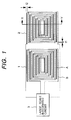
- Fig. 1 is a diagram showing the shape of coils of the invention.
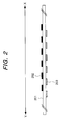
- Fig. 2 is a cross section of the coil shape of Fig. 1.
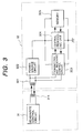
- Fig. 3 is a block diagram showing the circuit construction of the contactless IC card.
- the contactless IC card power and signals are transmitted and received between a coil 311 in a read/write control circuit 31 in a reader/writer (R/W) and a coil 321 in an IC card 32 having a communication control circuit by electromagnetic coupling.
- the IC card 32 comprises: a power source circuit 322 for generating a power voltage from an electromagnetic wave signal received by the coil 321; a transmitting and receiving control circuit 323 for controlling modulation/demodulation and transfer of the transmitted and received signals; a central processing unit (CPU) 324; and a memory 325.
- CPU central processing unit
- an RS232 transmitting data signal 610 is supplied from a CPU or the like to the read/write control circuit 31 and becomes a transmitting data signal 601.
- the transmitting data signal 601 is a serial signal and a logical signal of 0 and 1 and performs phase modulation (PSK modulation) of 180° to a carrier (4.91 MHz) signal.
- a PSK modulated data signal 602 passes through a filter circuit and the like, becomes a transmitting coil drive signal 603, and drives the transmitting coil 311.
- a received data signal 604 is obtained by the reception coil 321 electromagnetically connected to the coil on the transmitting side.
- the received data signal is converted to a binary form data signal 605 and processes such as demodulation are performed by the digital signal.
- a clock signal 606 is generated by using the binary form data signal 605 as a reference. By sampling the binary form data signal 605 at the leading edges of the clock signal 606, a demodulated signal 607 is obtained.
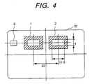
- the layout of the IC card according to the invention is as shown in Fig. 4 so as to follow ISO10536.
- the IC card 32 is constructed by an LSI 3 and coils 1 and 2.
- the LSI 3 has circuits 322 to 325 in Fig. 3.
- the coils 1 and 2 correspond to the coil 321 in Fig. 3.
- an area for transmitting and receiving signals is determined by two coils (coils 1 and 2) arranged at an interval of 22 mm (in the outer size of the coils) as shown in Fig. 4.
- the dimension of a coupling area in the coil is defined as about 11.6 mm ⁇ 4 mm from the relation with the reader/writer. Therefore, when the coils have to be formed in limited coil forming areas by printing means on a card, if the number of turns of the coil is large, it is necessary to narrow the line width of the printing pattern.
- Fig. 5 is a detailed diagram showing an example of two coils formed by silver paste printing.
- Each of the coils 1 and 2 is constructed by total 10 turns of five turns each on the surface and rear face.
- a solid line A shows the pattern on the surface and a broken line B shows the pattern on the rear face.
- the patterns on the surface and the rear face are connected via a through hole at a point C on the inner side of the coil.
- the silver paste coil has the pattern width of 150 ⁇ m, the thickness 20 of ⁇ m, and the pattern interval of 300 ⁇ m.
- the impedance (resistance) of the coil increases and the power is not easily obtained.
- a conductive paste such as silver paste
- the value of resistance in case of a coil having 20 turns and the line width of 150 ⁇ m is around 200 ⁇ and large, which is much larger than that of the etching coil.
- the internal resistance of the coil is a loss when the power is obtained.
- the power is 30 mW
- the loss by the coil is 20 mW. It is an order which cannot be ignored.
- Fig. 1 is a diagram showing a preferred embodiment of the invention.
- wiring t1 in the vertical direction of the antenna coils 1 and 2 having the coupling areas in the center has the line width of 150 ⁇ m same as that of Fig. 5 and the wiring line width t2 in the lateral direction is 300 ⁇ m which is wider than t1.
- the pattern in the vertical direction along the short side of the rectangular coupling area cannot be widened, because if it is widened, the coils 1 and 2 are short-circuited.
- the pattern in the lateral direction has dimensional room in the ISO standard and can be widened.
- the widths of the patterns in the vertical and lateral directions are varied as mentioned above, thereby enabling the impedance of the whole antenna coils to be further reduced.
- Fig. 2 is a cross sectional view taken on line X-Y of the antenna coil 2 in Fig. 1.
- Reference numeral 201 denotes a PET film having the thickness of 50 ⁇ m; 202 a silver paste printed coil on the surface; and 203 a silver paste printed coil on the rear face.
- the thickness of the film is thinner than that in case of performing an etching to a general substrate, so that a large floating capacity occurs.
- the floating capacity occurs between the wiring on the surface and that on the rear face, and the floating capacity and the coil form a resonant circuit.
- the resonant frequency is almost equal to the communication frequency, an adverse influence is exerted.
- the self resonant frequency in case of the above coil construction lies in a range from few MHz to tens MHz.
- the communication frequency of the power and signals of the contact IC card according to ISO10536 is defined as 4.91 MHz, so that the self resonant frequency is a problem.
- Fig. 2 shows the antenna coil constructed so as to reduce the influence of the floating capacity.
- the coil on the surface and the coil on the rear face are arranged to deviate from each other at a 1/2 pitch so as not to be in overlapped positions.
- the wiring pattern 203 of the coil on the rear side is arranged between the wiring of the coil pattern 202 on the surface.
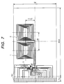
- Fig. 7 is a diagram showing the whole substrate (PET film substrate) of the IC card employing the invention.
- the dimension in the lateral direction of the antenna coils 1 and 2 is larger than that in the vertical direction.
- An integrated circuit is mounted in a position shown by 3.
- a terminal 701 is a test terminal for a circuit debug and is cut when the IC card is completed.
Landscapes
- Engineering & Computer Science (AREA)
- Computer Hardware Design (AREA)
- Microelectronics & Electronic Packaging (AREA)
- Physics & Mathematics (AREA)
- General Physics & Mathematics (AREA)
- Theoretical Computer Science (AREA)
- Computer Networks & Wireless Communication (AREA)
- Power Engineering (AREA)
- Credit Cards Or The Like (AREA)
- Near-Field Transmission Systems (AREA)
Applications Claiming Priority (3)
| Application Number | Priority Date | Filing Date | Title |
|---|---|---|---|
| JP1365097 | 1997-01-28 | ||
| JP1365097A JPH10203066A (ja) | 1997-01-28 | 1997-01-28 | 非接触icカード |
| JP13650/97 | 1997-01-28 |
Publications (2)
| Publication Number | Publication Date |
|---|---|
| EP0855674A2 true EP0855674A2 (de) | 1998-07-29 |
| EP0855674A3 EP0855674A3 (de) | 2005-08-31 |
Family
ID=11839112
Family Applications (1)
| Application Number | Title | Priority Date | Filing Date |
|---|---|---|---|
| EP98101385A Withdrawn EP0855674A3 (de) | 1997-01-28 | 1998-01-27 | Kontaktlose Chipkarte |
Country Status (4)
| Country | Link |
|---|---|
| US (2) | US5999409A (de) |
| EP (1) | EP0855674A3 (de) |
| JP (1) | JPH10203066A (de) |
| KR (1) | KR100470283B1 (de) |
Cited By (5)
| Publication number | Priority date | Publication date | Assignee | Title |
|---|---|---|---|---|
| EP1298578A4 (de) * | 2001-01-26 | 2005-05-11 | Sony Corp | Kontaktlose chipkarte |
| WO2006050363A1 (en) * | 2004-11-02 | 2006-05-11 | Precisia, L.L.C. | Variation of conductive cross section or material to enhance performance and reduce material consumption of electronic assemblies |
| EP1102256A3 (de) * | 1999-11-17 | 2006-10-04 | Sony Corporation | Aufzeichnungs- / Wiedergabegerät |
| CN101836330A (zh) * | 2007-10-24 | 2010-09-15 | 索尼化学&信息部件株式会社 | 天线电路及其电阻降低方法、以及应答器 |
| EP3879253A4 (de) * | 2018-12-17 | 2022-08-10 | Nagano Keiki Co., Ltd. | Rfid-antenne, rfid-etikett und vorrichtung zur messung der physikalischen quantität |
Families Citing this family (64)
| Publication number | Priority date | Publication date | Assignee | Title |
|---|---|---|---|---|
| DE19726335C2 (de) * | 1997-06-20 | 2000-03-02 | Angewandte Digital Elektronik | Chipkarte mit mindestens zwei Spulenanordnungen zur Übertragung von Daten und/oder Energie |
| DE19845065A1 (de) * | 1998-05-15 | 1999-11-25 | Siemens Ag | Vorrichtung zur kontaktlosen Übertragung von Daten |
| DE59913807D1 (de) * | 1998-06-23 | 2006-10-12 | Meto International Gmbh | Identifizierungselement |
| FR2784210B1 (fr) * | 1998-10-02 | 2001-09-14 | Gemplus Card Int | Carte a puce sans contact comportant des moyens d'inhibition |
| JP3643488B2 (ja) * | 1998-10-30 | 2005-04-27 | 株式会社日立製作所 | Icカード |
| US6373447B1 (en) * | 1998-12-28 | 2002-04-16 | Kawasaki Steel Corporation | On-chip antenna, and systems utilizing same |
| KR100530760B1 (ko) * | 1999-02-18 | 2005-11-23 | 삼성테크윈 주식회사 | 비접촉형 집적회로카드 및 그 제조방법 |
| US6650226B1 (en) | 1999-04-07 | 2003-11-18 | Stmicroelectronics S.A. | Detection, by an electromagnetic transponder reader, of the distance separating it from a transponder |
| FR2792135B1 (fr) | 1999-04-07 | 2001-11-02 | St Microelectronics Sa | Fonctionnement en complage tres proche d'un systeme a transpondeur electromagnetique |
| FR2792136B1 (fr) | 1999-04-07 | 2001-11-16 | St Microelectronics Sa | Transmission en duplex dans un systeme de transpondeurs electromagnetiques |
| FR2792132B1 (fr) | 1999-04-07 | 2001-11-02 | St Microelectronics Sa | Borne de lecture d'un transpondeur electromagnetique fonctionnant en couplage tres proche |
| JP3687459B2 (ja) * | 1999-06-29 | 2005-08-24 | ソニーケミカル株式会社 | Icカード |
| FR2796781A1 (fr) | 1999-07-20 | 2001-01-26 | St Microelectronics Sa | Dimensionnement d'un systeme a transpondeur electromagnetique pour un fonctionnement en hyperproximite |
| US7049935B1 (en) | 1999-07-20 | 2006-05-23 | Stmicroelectronics S.A. | Sizing of an electromagnetic transponder system for a dedicated distant coupling operation |
| JP2001084343A (ja) * | 1999-09-16 | 2001-03-30 | Toshiba Corp | 非接触icカード及びicカード通信システム |
| US6259408B1 (en) * | 1999-11-19 | 2001-07-10 | Intermec Ip Corp. | RFID transponders with paste antennas and flip-chip attachment |
| JP3822768B2 (ja) * | 1999-12-03 | 2006-09-20 | 株式会社ルネサステクノロジ | Icカードの製造方法 |
| US6396362B1 (en) * | 2000-01-10 | 2002-05-28 | International Business Machines Corporation | Compact multilayer BALUN for RF integrated circuits |
| JP3815936B2 (ja) * | 2000-01-25 | 2006-08-30 | 株式会社ルネサステクノロジ | Icカード |
| FR2804557B1 (fr) | 2000-01-31 | 2003-06-27 | St Microelectronics Sa | Adaptation de la puissance d'emission d'un lecteur de transpondeur electromagnetique |
| FR2808942B1 (fr) | 2000-05-12 | 2002-08-16 | St Microelectronics Sa | Validation de la presence d'un transpondeur electromagnetique dans le champ d'un lecteur a demodulation de phase |
| FR2808945B1 (fr) | 2000-05-12 | 2002-08-16 | St Microelectronics Sa | Evaluation du nombre de transpondeurs electromagnetiques dans le champ d'un lecteur |
| FR2808946A1 (fr) | 2000-05-12 | 2001-11-16 | St Microelectronics Sa | Validation de la presence d'un transpondeur electromagnetique dans le champ d'un lecteur |
| FR2808941B1 (fr) | 2000-05-12 | 2002-08-16 | St Microelectronics Sa | Validation de la presence d'un transpondeur electromagnetique dans le champ d'un lecteur a demodulation d'amplitude |
| FR2809235A1 (fr) | 2000-05-17 | 2001-11-23 | St Microelectronics Sa | Antenne de generation d'un champ electromagnetique pour transpondeur |
| FR2809251B1 (fr) | 2000-05-17 | 2003-08-15 | St Microelectronics Sa | Dispositif de production d'un champ electromagnetique pour transpondeur |
| US6400323B2 (en) * | 2000-06-23 | 2002-06-04 | Toyo Aluminium Kabushiki Kaisha | Antenna coil for IC card and manufacturing method thereof |
| JP2002026617A (ja) * | 2000-07-11 | 2002-01-25 | Murata Mfg Co Ltd | 伝送線路 |
| FR2812986B1 (fr) | 2000-08-09 | 2002-10-31 | St Microelectronics Sa | Detection d'une signature electrique d'un transpondeur electromagnetique |
| KR20010086181A (ko) * | 2001-07-13 | 2001-09-10 | 0 | 비접촉형 아이씨 모듈과 이를 장착한 아이씨 카드 |
| KR20030040986A (ko) * | 2001-11-19 | 2003-05-23 | (주)티오스 | 후막형 안테나를 이용한 초소형 비접촉식 전자 결제 카드 |
| JP4037703B2 (ja) * | 2002-06-28 | 2008-01-23 | 日本電気株式会社 | 内蔵アンテナ及び無線機 |
| JP4273734B2 (ja) * | 2002-09-25 | 2009-06-03 | ソニー株式会社 | アンテナ装置 |
| US6924777B2 (en) * | 2003-03-17 | 2005-08-02 | Hewlett-Packard Development Company, L.P. | Enhanced antenna using flexible circuitry |
| KR101204074B1 (ko) * | 2003-08-01 | 2012-11-27 | 삼성테크윈 주식회사 | 스마트 라벨 및, 그것의 제조 방법 |
| DE10356153B4 (de) * | 2003-12-02 | 2010-01-14 | Infineon Technologies Ag | Modul für kontaktlose Chipkarten oder Identifizierungssysteme |
| JP2005323288A (ja) * | 2004-05-11 | 2005-11-17 | Hosiden Corp | デジタルマイクロホン |
| US7604176B2 (en) * | 2004-05-20 | 2009-10-20 | American Express Travel Related Services Company, Inc. | Radio frequency fobs and methods of using the same |
| US7798415B1 (en) | 2004-05-20 | 2010-09-21 | American Express Travel Realted Services Company, Inc. | Wireless transaction fobs and methods of using the same |
| US20060000914A1 (en) * | 2004-06-30 | 2006-01-05 | Chen Chien-Yuan | Memory card capable of wireless transmission |
| KR101070908B1 (ko) * | 2004-10-25 | 2011-10-06 | 삼성테크윈 주식회사 | Rfid 태그 및 그 제조방법 |
| EP1701384A1 (de) * | 2005-03-08 | 2006-09-13 | Sun Microsystems France S.A. | Netzwerkplanung mit Halbleiterchips für Gitternetzkommunikation |
| US7688272B2 (en) * | 2005-05-30 | 2010-03-30 | Semiconductor Energy Laboratory Co., Ltd. | Semiconductor device |
| US7224278B2 (en) * | 2005-10-18 | 2007-05-29 | Avery Dennison Corporation | Label with electronic components and method of making same |
| US7881693B2 (en) | 2006-10-17 | 2011-02-01 | Semiconductor Energy Laboratory Co., Ltd. | Semiconductor device |
| US7701352B2 (en) * | 2006-11-22 | 2010-04-20 | Avery Dennison Corporation | RFID label with release liner window, and method of making |
| JP4847393B2 (ja) * | 2007-05-18 | 2011-12-28 | 株式会社東海理化電機製作所 | 無線通信機のアンテナ構造 |
| KR100826392B1 (ko) * | 2007-08-08 | 2008-05-02 | 삼성전기주식회사 | 이동 기기 및 그 제조 방법 |
| EP2188867A4 (de) * | 2007-09-13 | 2014-12-10 | Qualcomm Inc | Antennen für drahtlose energieanwendungen |
| US7926728B2 (en) * | 2007-10-31 | 2011-04-19 | Infineon Technologies Ag | Integrated circuit device including a contactless integrated circuit inlay |
| JP4314592B2 (ja) * | 2007-12-11 | 2009-08-19 | 日立化成工業株式会社 | Icカード |
| JP2008090863A (ja) * | 2007-12-11 | 2008-04-17 | Hitachi Chem Co Ltd | Icカード |
| JP4314591B2 (ja) * | 2007-12-11 | 2009-08-19 | 日立化成工業株式会社 | Icカード |
| WO2010001469A1 (ja) * | 2008-07-02 | 2010-01-07 | 三菱電機株式会社 | 無線通信装置 |
| JP4556002B2 (ja) * | 2008-10-14 | 2010-10-06 | 日立化成工業株式会社 | 非接触式icカード |
| US20110025463A1 (en) * | 2009-08-03 | 2011-02-03 | Atmel Corporation | Parallel Antennas for Contactless Device |
| EP2284985B1 (de) | 2009-08-10 | 2012-06-06 | Silicon Valley Micro M Corporation | Bürstenloser Gleichstrommotor mit RFID-Rotormagnet-Positionssensor |
| JP2010277609A (ja) * | 2010-09-01 | 2010-12-09 | Hitachi Chem Co Ltd | Icカード |
| KR20130023622A (ko) * | 2011-08-29 | 2013-03-08 | 삼성전기주식회사 | 도체 패턴 및 이를 포함하는 전자부품 |
| EP2575081B1 (de) | 2011-09-29 | 2019-04-10 | iMicrodata Corporation | Dokumentenverwaltung mithilfe eines fernen Dokumentenstandorts und Rückgewinnung |
| KR101514491B1 (ko) * | 2011-12-08 | 2015-04-23 | 삼성전기주식회사 | 코일 부품 및 그 제조방법 |
| WO2014088028A1 (ja) * | 2012-12-07 | 2014-06-12 | 株式会社村田製作所 | アンテナモジュール |
| US9214936B2 (en) * | 2013-06-18 | 2015-12-15 | Hyundai Motor Company | Non-contact sensing module and method of manufacturing the same |
| JP7112815B2 (ja) * | 2017-03-10 | 2022-08-04 | サトーホールディングス株式会社 | 容器のラベル |
Family Cites Families (19)
| Publication number | Priority date | Publication date | Assignee | Title |
|---|---|---|---|---|
| US4016519A (en) * | 1976-05-14 | 1977-04-05 | Blaupunkt-Werke Gmbh | Printed circuit coils |
| US4583099A (en) * | 1983-12-27 | 1986-04-15 | Polyonics Corporation | Resonant tag circuits useful in electronic security systems |
| US4795898A (en) * | 1986-04-28 | 1989-01-03 | American Telephone And Telegraph Company | Personal memory card having a contactless interface using differential data transfer |
| US4926292A (en) * | 1989-08-09 | 1990-05-15 | Avantek, Inc. | Broadband printed spiral |
| WO1992013372A1 (en) * | 1991-01-24 | 1992-08-06 | Rdi Electronics, Inc. | Broadband antenna |
| US5237165A (en) * | 1991-04-05 | 1993-08-17 | Tingley Iii Loyal H | Multi-turn coil structures and methods of winding same |
| JPH04325293A (ja) * | 1991-04-25 | 1992-11-13 | Mitsubishi Electric Corp | 非接触icカード |
| JPH05128324A (ja) * | 1991-11-07 | 1993-05-25 | Mitsubishi Electric Corp | 非接触カード、非接触カード用端末機及び非接触伝送システム |
| FR2691563B1 (fr) * | 1992-05-19 | 1996-05-31 | Francois Droz | Carte comprenant au moins un element electronique et procede de fabrication d'une telle carte. |
| JP2713529B2 (ja) * | 1992-08-21 | 1998-02-16 | 三菱電機株式会社 | 信号受信用コイルおよびこれを使用した非接触icカード |
| JPH07120237A (ja) * | 1993-10-22 | 1995-05-12 | Nichiden Mach Ltd | 画像認識装置 |
| FR2716281B1 (fr) * | 1994-02-14 | 1996-05-03 | Gemplus Card Int | Procédé de fabrication d'une carte sans contact. |
| FR2727225B1 (fr) * | 1994-11-22 | 1997-01-24 | Innovatron Ind Sa | Objet portatif comprenant un circuit electronique alimente par pile interne et comportant une memoire de donnees, procede et dispositif d'alimentation externe de cet objet et de transfert de donnees avec celui-ci |
| JPH08216570A (ja) * | 1995-02-09 | 1996-08-27 | Hitachi Chem Co Ltd | Icカード |
| JP2814477B2 (ja) * | 1995-04-13 | 1998-10-22 | ソニーケミカル株式会社 | 非接触式icカード及びその製造方法 |
| JP3639641B2 (ja) * | 1995-06-06 | 2005-04-20 | 大日本印刷株式会社 | 非接触icカードおよびその製造方法 |
| JPH091970A (ja) * | 1995-06-20 | 1997-01-07 | Hitachi Chem Co Ltd | Icカード及びその製造法 |
| JP3725599B2 (ja) * | 1995-09-07 | 2005-12-14 | 株式会社東芝 | 平面型磁気素子 |
| FR2743649B1 (fr) * | 1996-01-17 | 1998-04-03 | Gemplus Card Int | Module electronique sans contact, carte etiquette electronique l'incorporant, et leurs procedes de fabrication |
-
1997
- 1997-01-28 JP JP1365097A patent/JPH10203066A/ja active Pending
-
1998
- 1998-01-21 US US09/010,184 patent/US5999409A/en not_active Expired - Fee Related
- 1998-01-22 KR KR10-1998-0001848A patent/KR100470283B1/ko not_active Expired - Fee Related
- 1998-01-27 EP EP98101385A patent/EP0855674A3/de not_active Withdrawn
-
1999
- 1999-08-13 US US09/373,722 patent/US6373708B1/en not_active Expired - Fee Related
Cited By (11)
| Publication number | Priority date | Publication date | Assignee | Title |
|---|---|---|---|---|
| EP1102256A3 (de) * | 1999-11-17 | 2006-10-04 | Sony Corporation | Aufzeichnungs- / Wiedergabegerät |
| EP1298578A4 (de) * | 2001-01-26 | 2005-05-11 | Sony Corp | Kontaktlose chipkarte |
| US6950074B2 (en) | 2001-01-26 | 2005-09-27 | Sony Corporation | Noncontact type IC card |
| EP1965338A1 (de) * | 2001-01-26 | 2008-09-03 | Sony Corporation | Kontaktfreie IC-Karte |
| WO2006050363A1 (en) * | 2004-11-02 | 2006-05-11 | Precisia, L.L.C. | Variation of conductive cross section or material to enhance performance and reduce material consumption of electronic assemblies |
| GB2435183A (en) * | 2004-11-02 | 2007-08-15 | Precisia L L C | Variation of conductive cross section or material to enchance performance and reduce material comsumption of electronic assemblies |
| US7323993B2 (en) | 2004-11-02 | 2008-01-29 | Zih Corp. | Variation of conductive cross section and/or material to enhance performance and/or reduce material consumption of electronic assemblies |
| GB2435183B (en) * | 2004-11-02 | 2009-12-02 | Precisia L L C | Variation of conductive cross section or material to enchance performance and reduce material comsumption of electronic assemblies |
| CN101836330A (zh) * | 2007-10-24 | 2010-09-15 | 索尼化学&信息部件株式会社 | 天线电路及其电阻降低方法、以及应答器 |
| CN101836330B (zh) * | 2007-10-24 | 2014-05-28 | 迪睿合电子材料有限公司 | 天线电路及其电阻降低方法、以及应答器 |
| EP3879253A4 (de) * | 2018-12-17 | 2022-08-10 | Nagano Keiki Co., Ltd. | Rfid-antenne, rfid-etikett und vorrichtung zur messung der physikalischen quantität |
Also Published As
| Publication number | Publication date |
|---|---|
| KR100470283B1 (ko) | 2005-03-16 |
| US5999409A (en) | 1999-12-07 |
| JPH10203066A (ja) | 1998-08-04 |
| KR19980070698A (ko) | 1998-10-26 |
| US6373708B1 (en) | 2002-04-16 |
| EP0855674A3 (de) | 2005-08-31 |
Similar Documents
| Publication | Publication Date | Title |
|---|---|---|
| US5999409A (en) | Contactless IC card | |
| TWI474553B (zh) | 天線電路以及傳輸器 | |
| JP4641096B2 (ja) | 非接触式データキャリア装置とブースターアンテナ部用配線部材 | |
| JP3915092B2 (ja) | Icカード用のブースタアンテナ | |
| US7126482B2 (en) | RFID tag and its manufacturing method | |
| US8814056B2 (en) | Antenna device, RFID tag, and communication terminal apparatus | |
| JPH11149536A (ja) | 複合icカード | |
| JPWO2001085469A1 (ja) | 非接触式データキャリア装置 | |
| KR20060103425A (ko) | 플랫 스톡으로 만들어진 3차원 안테나 배열이 있는 보안태그 및 그 제조 방법 | |
| JP2004062854A (ja) | Icモジュール及びこれを用いた無線情報記憶媒体並びに無線情報送受信装置 | |
| JP4114446B2 (ja) | アンテナ装置及びこれを用いた読み出し書き込み装置、情報処理装置、通信方法並びにアンテナ装置の製造方法 | |
| JPH11353440A (ja) | コンデンサ及び非接触型icカード | |
| JP4562892B2 (ja) | 非接触式データキャリア装置とブースターアンテナ部用配線部材 | |
| EP3014531B1 (de) | Kartenkörper und chipkarte mit diesem körper | |
| JP2010028351A (ja) | ブースターアンテナ及び非接触情報媒体 | |
| JP2000172814A (ja) | 複合icモジュール及び複合icカード | |
| JP4643112B2 (ja) | データライブラリ認識装置及びデータライブラリ認識システム | |
| JP4641095B2 (ja) | 非接触式データキャリア装置とブースターアンテナ部用配線部材 | |
| JP2003006589A (ja) | 非接触通信記録媒体及びその製造方法 | |
| JP4724923B2 (ja) | 接触・非接触兼用型icモジュールとその製造方法 | |
| JPH04292998A (ja) | Icカード | |
| JP4684430B2 (ja) | 接触・非接触兼用型icモジュールとその製造方法 | |
| JP2001202488A (ja) | 非接触icタグ | |
| JPH11161763A (ja) | アンテナ回路を具備した非接触型カード媒体および製造方法 | |
| JP2004364143A (ja) | アンテナシート、icカード及びコンデンサの形成方法 |
Legal Events
| Date | Code | Title | Description |
|---|---|---|---|
| PUAI | Public reference made under article 153(3) epc to a published international application that has entered the european phase |
Free format text: ORIGINAL CODE: 0009012 |
|
| AK | Designated contracting states |
Kind code of ref document: A2 Designated state(s): AT BE CH DE DK ES FI FR GB GR IE IT LI LU MC NL PT SE |
|
| AX | Request for extension of the european patent |
Free format text: AL;LT;LV;MK;RO;SI |
|
| PUAL | Search report despatched |
Free format text: ORIGINAL CODE: 0009013 |
|
| AK | Designated contracting states |
Kind code of ref document: A3 Designated state(s): AT BE CH DE DK ES FI FR GB GR IE IT LI LU MC NL PT SE |
|
| AX | Request for extension of the european patent |
Extension state: AL LT LV MK RO SI |
|
| STAA | Information on the status of an ep patent application or granted ep patent |
Free format text: STATUS: THE APPLICATION HAS BEEN WITHDRAWN |
|
| 18W | Application withdrawn |
Effective date: 20051013 |