EP0862193A2 - Schichtverbundes elektronisches Bauelement und sein Herstellungsverfahren - Google Patents
Schichtverbundes elektronisches Bauelement und sein Herstellungsverfahren Download PDFInfo
- Publication number
- EP0862193A2 EP0862193A2 EP98102233A EP98102233A EP0862193A2 EP 0862193 A2 EP0862193 A2 EP 0862193A2 EP 98102233 A EP98102233 A EP 98102233A EP 98102233 A EP98102233 A EP 98102233A EP 0862193 A2 EP0862193 A2 EP 0862193A2
- Authority
- EP
- European Patent Office
- Prior art keywords
- ceramic
- ceramic layers
- layers
- thermal expansion
- magnetic
- Prior art date
- Legal status (The legal status is an assumption and is not a legal conclusion. Google has not performed a legal analysis and makes no representation as to the accuracy of the status listed.)
- Withdrawn
Links
Images
Classifications
-
- H—ELECTRICITY
- H01—ELECTRIC ELEMENTS
- H01F—MAGNETS; INDUCTANCES; TRANSFORMERS; SELECTION OF MATERIALS FOR THEIR MAGNETIC PROPERTIES
- H01F17/00—Fixed inductances of the signal type
- H01F17/0006—Printed inductances
- H01F17/0013—Printed inductances with stacked layers
-
- H—ELECTRICITY
- H01—ELECTRIC ELEMENTS
- H01F—MAGNETS; INDUCTANCES; TRANSFORMERS; SELECTION OF MATERIALS FOR THEIR MAGNETIC PROPERTIES
- H01F41/00—Apparatus or processes specially adapted for manufacturing or assembling magnets, inductances or transformers; Apparatus or processes specially adapted for manufacturing materials characterised by their magnetic properties
- H01F41/02—Apparatus or processes specially adapted for manufacturing or assembling magnets, inductances or transformers; Apparatus or processes specially adapted for manufacturing materials characterised by their magnetic properties for manufacturing cores, coils, or magnets
- H01F41/04—Apparatus or processes specially adapted for manufacturing or assembling magnets, inductances or transformers; Apparatus or processes specially adapted for manufacturing materials characterised by their magnetic properties for manufacturing cores, coils, or magnets for manufacturing coils
- H01F41/041—Printed circuit coils
- H01F41/046—Printed circuit coils structurally combined with ferromagnetic material
-
- H—ELECTRICITY
- H01—ELECTRIC ELEMENTS
- H01F—MAGNETS; INDUCTANCES; TRANSFORMERS; SELECTION OF MATERIALS FOR THEIR MAGNETIC PROPERTIES
- H01F17/00—Fixed inductances of the signal type
- H01F17/0006—Printed inductances
- H01F17/0013—Printed inductances with stacked layers
- H01F2017/0026—Multilayer LC-filter
-
- Y—GENERAL TAGGING OF NEW TECHNOLOGICAL DEVELOPMENTS; GENERAL TAGGING OF CROSS-SECTIONAL TECHNOLOGIES SPANNING OVER SEVERAL SECTIONS OF THE IPC; TECHNICAL SUBJECTS COVERED BY FORMER USPC CROSS-REFERENCE ART COLLECTIONS [XRACs] AND DIGESTS
- Y10—TECHNICAL SUBJECTS COVERED BY FORMER USPC
- Y10T—TECHNICAL SUBJECTS COVERED BY FORMER US CLASSIFICATION
- Y10T428/00—Stock material or miscellaneous articles
- Y10T428/24—Structurally defined web or sheet [e.g., overall dimension, etc.]
- Y10T428/24942—Structurally defined web or sheet [e.g., overall dimension, etc.] including components having same physical characteristic in differing degree
Definitions
- the present invention relates to a laminated composite electronic device constructed with different kinds of ceramic layers, such as magnetic ceramic and dielectric ceramic, and in particular to a laminated composite electronic device combining an inductance portion, in which an internal electrodes are formed in a spiral shape in the laminated magnetic ceramic layers, with a capacitor portion, in which a pair of internal electrodes opposing to each other are formed within the laminated dielectric ceramic layers.
- a slurry build method In manufacturing electronic devices of a laminated composite type, there are available two kinds of methods for obtaining a laminated body, one of which is so-called a slurry build method and the other of which is so-called a sheet method.
- a slurry build method of the former magnetic paste and electric conductive paste are printed over one by one with a method of such as a screen printing so as to form the magnetic material layers and an internal electrode pattern of the spiral shape therein, and a dielectric paste and the electric conductive paste are also printed over one by one to form the dielectric materiallayers and a pair of internal electrode patterns opposing to each other therein.
- the magnetic ceramic green sheets on which the internal electrode patterns are printed in the spiral shape with the electric conductive paste in advance by such the screen printing method are piled over, and the dielectric sheets on which the opposing internal electrodes are printed with the electric conductive paste in advance are also piled over.
- the internal electrode patterns formed on the magnetic ceramic green sheets are connected one by one in the spiral shape via electric conduction by means of so-called through-holes which are also provided on the magnetic ceramic green sheets in advance.
- the laminated body which is obtained by either one of the methods mentioned in the above is ultimately baked, and the electric conductive paste is also baked after being printed on both side surfaces on which the electric conductive bodies are exposed to form external electrodes thereof.
- the laminated composite electronic device can be obtained.
- the magnetic material layers and the dielectric material layers are piled up or laminated as an unit. Further, in the magnetic material layers is formed the coil-shaped internal electrode piling up spirally in a direction of lamination thereof, and a part the internal electrode is connected to the external electrode at an edge portion of laminated body mentioned above.
- At least one pair of internal electrodes are formed, opposing to each other through the same layer(s), and those internal electrodes are extended or led out to the opposing edge surfaces of the laminated body to be electrically connected to the external electrodes, respectively.
- the inductor and the capacitor are connected in a predetermined condition through the external electrodes.
- Such the laminated composite electronic device in the manufacturing process thereof, is made by baking the laminated body of the different kinds of ceramic layers at a high temperature, in the condition of joining them together and is cooled down thereafter.
- the different kinds of ceramics show the respective thermal expansion rate thereof, being different greatly to each other, in particular, such as between the magnetic ceramic layers and the dielectric ceramic layers. Then, because of the differences in the thermal expansion or shrinkage between the respective ceramic layers of the laminated body formed by baking, thermal stress occurs inside of the laminated body during a cooling process after the baking, thereby being distorted the laminated body in the shape and causing cracks inside thereof.
- An object in accordance with the present invention is, for dissolving such the problems in the conventional manufacturing process of such the laminated composite electronic devices, to provide a laminated composite electronic device and a manufacturing process thereof, with which the laminated body of the laminated composite electronic device can be baked without causing such the deformation and the cracks therein.
- a laminated composite electronic device in which laminated intermediate ceramic layers a, b, c and d, being different in thermal expansion rate gradually and in stepwise one another, are inserted between the neighboring ceramic layers of a laminated body 11 so as to reduce the difference in the thermal expansion rate between them.
- a manufacturing method of the laminated composite electronic device in which ceramic green sheets are piled up in such a manner that the laminated intermediate ceramic layers a, b, c and d, being different in the thermal expansion rate gradually and stepwise one another, are inserted between the ceramic green sheets forming the ceramic layers 1, 1' and 7, 7' of the different kinds, also being different in the thermal expansion rate thereof to each other.
- this laminated composite electronic device it is possible to prevent the laminated body 11 from the thermal stress caused by the difference in the thermal expansion rate between the ceramic layers 1, 1' and 7, 7' of the different kinds during the cooling process after the baking thereof. Thereby, it is possible to protect the laminated composite electronic device from the deformation, such as a curve, and cracks in the laminated body 11 thereof.
- the laminated composite electronic device in accordance with the present invention, can be characterized by that the intermediate ceramic layers a, b, c and d, being different in thermal expansion rate in stepwise one another, are positioned between the ceramic layers 1, 1' and 7, 7' of different kinds, so as to reduce the difference in the thermal expansion rate between the neighboring ceramic layers of the laminated body 11 in the laminated composite electronic device which has the different kinds of laminated ceramic layers 1, 1' and 7, 7' differing from in the thermal expansion rate thereof.
- the dielectric ceramic layers and the magnetic ceramic layers can be referred.
- a glass component is added thereto, as the most effective example of the components for adjusting the thermal expansion rate thereof, which has the thermal expansion rate differing from both the magnetic ceramic and the dielectric ceramic. Namely, by adjusting the thermal expansion rate with the components which is obtained by adding the glass component to that of either one of the different kinds of the ceramic layers 1, 1' or 7, 7' mentioned above, the plurality of the intermediate ceramic layers a, b, c and d which differ from in thermal expansion rate gradually and in stepwise one another can be obtained.
- the difference in the thermal expansion rate between the neighboring ceramic layers in the laminated body 11 comes to be small.
- the thermal stress in the laminated body 11 can be released, as well as the deformation such as a curvature and the cracks inside thereof and so on can be prevented from occurring in the cooling process after the baking.
- the intermediate ceramic layers a, b, c and d differ from in the thermal expansion rate gradually and in stepwise one another, the thermal expansion rates of those respective ceramic layers forming the laminated body 11 also change gradually, thereby it is possible to reduce that difference between the neighboring ceramic layers.
- the difference in the thermal expansion rate to another neighboring ceramic layers is also large, it is necessary to appropriately change the thickness of the layer(s) of the intermediate ceramic layers a, b, c and d at that portion, such as by making it thicker.
- the intermediate ceramic layers a, b, c and d mentioned above contain the same component to the principal one of the ceramic layers of either one of the different kind ceramic layers 1, 1' or 7, 7', and the thermal expansion rate can be adjusted by changing the composition rate of the components thereof.
- magnetic ceramics of ferrite group such as Fe 2 O 3 , NiO, ZnO and CuO can be referred.
- the thermal expansion rate thereof is appropriately adjusted.
- a manufacturing method of such the laminated composite electronic device has steps of piling up different kinds of ceramic green sheets to form a laminated body; and baking said laminated body, wherein the intermediate ceramic layers of the ceramic green sheet differing from in the thermal expansion rate gradually and stepwise one another are formed, so as to reduce the difference in the thermal expansion rate between the neighboring ceramic layers of the laminated body 11, and the formed intermediate ceramic layers of the ceramic green sheets are inserted between the ceramic green sheets forming the different kind ceramic layers 1, 1' and 7, 7' differing from each other in the thermal expansion rate, when the ceramic green sheets are piled up.
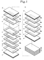
- Fig. 1 shows construction of a laminated body of a laminated composite electronic device, in particular of a LC element.
- the laminated body mentioned above is manufactured at the same time in a large number by the following manners.
- thin magnetic ceramic green sheets are formed of magnetic slurry which is obtained by dispersing powder of magnetic material, such as ferrite powder into binder, by using a method of so-called a doctor blade method or an extruder. At predetermined positions on the ceramic green sheets are punched or penetrated the through-holes in advance. After that, internal electrode patterns are printed on the ceramic green sheets, with an electric conductive paste such as the silver paste, aligning them in vertical and/or horizontal directions in circular, for a large number of sets thereof, and the conductive paste is vacuumed through and printed on inner surfaces of those through-holes as the conductor thereof.
- an electric conductive paste such as the silver paste
- dielectric ceramic green sheets containing powder of dielectric material, such as titanium oxide, etc. interior electrode patterns are printed on a part of those ceramic green sheets, with aligning them in vertical or horizontal direction, for a large number of sets thereof.
- ceramic green sheets other than those magnetic ceramic green sheets and those dielectric ceramic green sheets, are prepared so as to form ceramic layers having thermal expansion rate in the middle of those of the ceramics.
- the coefficient of linear expansion of the magnetic ceramic containing Fe 2 O 3 of 49 mol%, NiO of 42 mol%, ZnO of 4 mol% and CuO of 5 mol% is 13.0 ⁇ 10 -6 /°C
- the coefficient of linear expansion of the dielectric ceramic mainly containing TiO 2 is 8.5 ⁇ 10 -6 /°C.
- the magnetic ceramic mentioned above shows the thermal expansion rate decreasing if the composition of ZnO is increased in spite of the composition of NiO of the components mentioned above, therefore, it is also possible to obtain the ceramic showing the thermal expansion rate laying in the middle of those of the magnetic ceramic and the dielectric ceramic.
- the green sheets are prepared in advance for intermediate layers, each of which shows different coefficient of linear expansion in stepwise within a range between those of the magnetic ceramic and the dielectric ceramic.
- the thinner the thickness of the intermediate layer of the laminated body the more finely can be divided in stepwise the difference in the coefficient of linear expansion between those of the magnetic ceramic and the dielectric ceramic, therefore, a large number of the intermediate ceramic green sheets are prepared for reducing the difference, in advance.
- the thicker ceramic green sheets are prepared for forming the thicker intermediate layers.
- those ceramic green sheets are piled up.
- a few or several number of the magnetic ceramic green sheets are piled up, on the surface of which no internal electrode pattern is printed, and then a number of ceramic green sheets, on the surface of which different kinds of the internal electrode patterns are printed receptively, are piled up one by one, depending on the number of turns of a necessary coil to be formed.
- those ceramic green sheets laminated are further piled up with a few or several number of the magnetic ceramic green sheets, on the surface of which no internal electrode pattern is printed, again.
- the ceramic green sheets containing the ceramic which has the adjusted coefficient of linear expansion lying in the middle of the magnetic ceramic and the dielectric ceramic in the manner mentioned above, are piled upon them.
- the coefficient of linear expansion of the dielectric ceramic is smaller than that of the magnetic ceramic, therefore, the ceramic green sheets are piled up successively in the order from the ceramic having the larger coefficient of linear expansion to the smaller one, in this example of those ceramic green sheets.
- the sequential order of compiling the dielectric ceramic green sheets and the magnetic green sheets can be reversed upside down. Namely, it is needless to say that the dielectric ceramic green sheets can be compiled first and then the magnetic ceramic green sheets thereon afterward.
- the laminated body obtained in the above, after being pressed to be contacted or joined therein, is cut and divided into each chip, and the laminated chip is baked to be obtained as the baked laminated body 11.
- the laminated body 11 obtained in this manner has a plurality of laminated ceramic layers 1, 1..., 1', 1'... formed as an unit or a body, and the layer construction thereof is shown in Fig. 1.
- the ceramic layers 1, 1 ... made of magnetic ceramic form magnetic core of the coil obtained.
- the internal electrodes 5e and 5f which are formed on the ceramic layers 1 and 1 at the top and the bottom among the ceramic layers 1, 1 ... including the internal electrodes 5a, 5b ..., are extended and led onto a pair of opposing end surfaces of the laminated body 11.
- the intermediate ceramic layers a, b, c and d each having respective thermal expansion rate differing in stepwise one another in the range between those of the magnetic ceramic layers 1, 1' and the dielectric ceramic layers 7, 7' which are piled thereon.
- the layer d at the lowest of the intermediate layers has the thermal expansion rate which is a little bit smaller than that of the magnetic ceramic layers 1, 1', and the other intermediate layers c, b and a have the respective thermal expansion rates increasing from it sequentially in stepwise.
- the layer a at the top of the intermediate layers has the thermal expansion rate being a little bit higher than that of the dielectric ceramic layers 7, 7'.
- the dielectric ceramic layer 7' of so-called blank is piled up, and the dielectric ceramic layers 7, 7 ... having the internal electrodes 8a and 8b are piled up on it. And, further on them, there is piled with the dielectric ceramic layers 7' without the internal electrodes 8a and 8b.
- Those internal electrodes 8a and 8b provided in the dielectric ceramic layers 7, 7 ... are opposing to each other through the same ceramic layers 7, 7 ... and are alternately led to a pair of the opposing edge surfaces of the laminated body 11, on which the internal electrodes 5e and 5f are extended.
- the electric conductive paste such as the silver paste
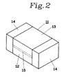
- the electric conductive paste is painted to be baked, and further are formed with external electrodes 14 and 14 provided by nickel plating or solder thereon, if necessary.
- the above-mentioned internal electrodes 5e, 5f, 8a and 8b (refer Fig. 1) which are extended onto the edge surfaces of the laminated body 11.
- the inductance formed by the internal electrodes 5a, 5b ... and the dielectric capacitance obtained by the opposing internal electrodes 8a and 8b are connected in parallel to each other through the external electrodes 14 and 14.
- a reference numeral 12 denotes a laminated layer portion of the magnetic ceramic layers having the inductance formed therein by piling up the magnetic ceramic layers 1, 1'
- a reference numeral 13 a laminated layer portion of the dielectric ceramic layers having the capacitance formed therein by piling up the dielectric ceramic layers 7, 7'
- a reference numeral 15 a laminated layer portion of intermediate ceramic layers, which have the thermal expansion rates differing from one another in stepwise between those of the magnetic ceramic layers 1, 1' and the dielectric ceramic layers 7, 7' and are formed by piling up the intermediate layers a, b, c and d.
- the laminated composite electronic device even if the laminated layer portion 12 of the magnetic ceramic layers differs from the laminated layer portion 13 of the dielectric ceramic layers in the thermal expansion rate, the heat shock occurring in the cooling process after the baking is absorbed by the laminated layer portion 15 of the intermediate ceramic layers which is formed by compiling the intermediate layers a, b, c and d differing from one another in stepwise in the thermal expansion rates thereof, thereby hardly causing the deformation such as the curving and/or the cracks in the laminated body 11.
- Raw material powders are prepared at the rate, Fe 2 O 3 of 49 mol%, NiO of 42 mol%, ZnO of 42 mol% and CuO of 5 mol%, for the magnetic powder of the ferrite group, and they are dispersed into the organic binder so as to make the magnetic slurry after they are pre-baked at the temperature of 680 °C respectively.
- the magnetic slurry is formed into the magnetic ceramic green sheet of the thickness of 30 ⁇ m by the doctor blade method.
- the coefficient of linear expansion of the magnetic ceramic, being formed by baking the magnetic ceramic green sheet as will be mentioned later, is 13.0 ⁇ 10 -6 /°C.
- the internal electrodes of the silver paste are printed aligning in vertical and/or horizontal directions in circular on the large number of sets thereof, and the silver paste is vacuumed through and printed on the inner surface of those through-holes as the conductor thereof.
- the dielectric ceramic power mainly containing TiO 2 is prepared, and the dielectric ceramic green sheets are formed in the same manner mentioned in the above.
- the silver paste are printed as the internal electrode patterns aligning in vertical and/or horizontal directions on the large number of sets thereof.
- the coefficient of the linear expansion of the dielectric ceramic, being formed by baking the dielectric ceramic green sheet as will be mentioned later, is 8.5 ⁇ 10 -6 /°C, and has a difference of 4.5 ⁇ 10 -6 /°C from that of the magnetic ceramic mentioned in the above.
- the dielectric material mainly containing the TiO 2 powder with glass powder having composition of SiO 2 of 46.1 weight%, B 2 O 3 of 1.5 weight%, Na 2 O of 19.8 weight%, K 2 O of 21.2 weight%, BaO of 9.9 weight% and ZnO of 1.5 weight%, by the amounts shown in Table 1 below with respect to the weight of the dielectric ceramic material, four (4) kinds of the dielectric-glass ceramic green sheets A, B, C and D are formed.
- the coefficient of linear expansion of the glass of the compositions mentioned above is 16 ⁇ 10 -6 /°C, being larger than that of the magnetic ceramic, as well as that of the dielectric ceramic of course.
- the coefficients of the linear expansion of the intermediate ceramic layers a, b, c and d are shown, which are formed by baking the above-mentioned dielectric-glass ceramic green sheets A, B, C and D.
- the coefficients of the linear expansion of the magnetic ceramic layer and the dielectric ceramic layer are also shown in it.
- Ceramic Material Add Amount of Glass Coefficient of Linear Expansion Dielectric Material 0 weight% 8.5 ⁇ 10 - 6/°C Dielectric-Glass A 13.3 weight% 9.6 ⁇ 10 - 6/°C Dielectric-Glass B 26.7 weight% 10.3 ⁇ 10 - 6/°C Dielectric-Glass C 40.0 weight% 11.4 ⁇ 10 - 6/°C Dielectric-Glass D 53.3 weight% 12.4 ⁇ 10 - 6/°C Magnetic Material -- 13.0 ⁇ 10 - 6/°C
- the magnetic ceramic green sheets of the blank on which no such the internal electrode pattern is printed are piled up, and then further on those are piled up the magnetic ceramic green sheets which are printed with the internal electrode patterns, one by one, in such manner that the coil is formed by those internal electrode patterns being connected in spiral with the through-holes. Further, on those magnetic ceramic green sheets, the magnetic ceramic green sheets of the blank with no such the printed internal electrode pattern are piled up again.
- dielectric-glass ceramic green sheets are piled up several pieces of the dielectric ceramic green sheets on which no infernal electrode pattern is printed.
- dielectric ceramic green sheets are piled up alternately, each of which has the internal electrode pattern shifting one another. Further on those are piled up again with dielectric ceramic green sheets on which no infernal electrode pattern is printed.
- the laminated body of those after being suppressed with a pressure 390 Kgf/cm 2 to joint them as an unit, is cut into respected chips.
- Those laminated chips which are not baked yet are treated with at a temperature of 500 °C so as to remove the binder therefrom, and thereafter they are baked at a temperature of 890 °C ,thereby obtaining a thousand of chips of the laminated body 11 as shown in Fig. 1
- the magnetic ceramic layers 1, 1 ... and the magnetic ceramic layers 1', 1' ... are formed by baking the magnetic ceramic green sheets mentioned in the above.
- the intermediate ceramic layers a, b, c and d are formed by baking the above-mentioned respective dielectric-glass ceramic green sheets A, B, C and D.
- the dielectric ceramic layers 7, 7 ... and the dielectric ceramic layers 7', 7'... are formed by baking the dielectric ceramic green sheets mentioned above.
- the thickness of the respective layers of the magnetic ceramic layers 1, 1', of the intermediate ceramic layers a, b, c and d, and of the magnetic ceramic layers 7 and 7' are shown in Table 2 below, in particular in the column for a sample No. 4 thereof.
- the laminated composite electronic device having such configure as shown in Fig. 2 is completed.
- the laminated bodies 11 shown in the Table 2 in particular in the columns for the sample Nos. 1 to 3, 5 and 6 thereof, are obtained, by piling up no dielectric-glass ceramic green sheet for forming the intermediate ceramic layers a, b, c and d, and by changing the combination of the dielectric-glass ceramic green sheets for forming the intermediate ceramic layers a, b, c and d, in the same manner as mentioned in the above, they are also checked or tested for the presence of the cracks. And, the result of the testing are shown in the Table 2, in the respective columns of the sample Nos. 1 to 3, 5 and 6 thereof.
- the number of occurrence of the cracks in the laminated body 11 is zero (0) on both the sample No. 4 in which the intermediate layers a, b, c and d differing from in four steps in the coefficients of linear expansion and having thickness of 45 ⁇ m are inserted between the magnetic ceramic layers 1, 1' and the dielectric ceramic layers 7, 7', and the sample No. 5 in which the intermediate layers a, b and c differing from in three steps in the coefficients of linear expansion and having thickness of 45 ⁇ m are inserted between the magnetic ceramic layers 1, 1' and the dielectric ceramic layers 7, 7'.
- the difference among those ceramic layers is less than 2 ⁇ 10 -6 /°C for both of them.
- no crack occurs in the laminated body 11.
- the difference among those ceramic layers is also small, being such as 2 ⁇ 10 -6 /°C.
- the cracks occur with high frequency, for example on the samples Nos. 1 and 3 in which the difference in the coefficient of linear expansion between the magnetic ceramic layers 1, 1' and the dielectric ceramic layers 7, 7' exceeds that value, i.e., 2 ⁇ 10 -6 /°C.
- the sample No. 6 in which the intermediate layers a and d of two steps are inserted between the magnetic ceramic layers 1, 1' and the dielectric ceramic layers 7, 7', since the difference in the coefficient of linear expansion between those intermediate layers a and d exceeds 2 ⁇ 10 -6 /°C, therefore, the cracks occurs with high frequency in the laminated body 11.
- the laminated body 11 can be protected from the cracks occurring therein, effectively by suppressing the differences in the coefficient of linear expansion thereof, between the magnetic ceramic layers 1, 1' and the intermediate ceramic layer a, between the dielectric ceramic layers 7, 7' and the intermediate ceramic layer d, and also among the intermediate ceramic layers a, b, c and d, being less than 2 ⁇ 10 -6 /°C.
- four (4) kinds of magnetic-glass ceramic green sheets A, B, C and D are prepared by adding glass powder of Si-B group (i.e., aluminoborosilicate glass) having the coefficient of linear expansion of 5 ⁇ 10 -6 /°C into the magnetic ceramic material, by such amount as shown in Table 3 below with respect to the weight of the magnetic ceramic material, respectively.
- Si-B group i.e., aluminoborosilicate glass
- Table 3 the coefficients of linear expansion of each of the intermediate glass ceramic layers a, b, c and d are also shown, which are manufactured in such a manner as will be mentioned later.
- the magnetic ceramic layers containing no glass component are not piled up, however, in place of those, the above-mentioned magnetic-glass ceramic green sheet B from which can be obtained the ceramic having coefficient of linear expansion of 10.4 ⁇ 10 -6 /°C, and the above-mentioned magnetic-glass ceramic green sheet C from which can be obtained the ceramic having coefficient of linear expansion of 11.3 ⁇ 10 -6 /°C, are used to form the laminated body.
- Thickness of Magnetic Layers ( ⁇ m) Thickness of Intermediate Layers ( ⁇ m) A B C D 1 600 - - - - 2 600 - 600 - - 3 600 - - 600 - 4 600 50 50 50 50 5 600 50 - 50 50 6 600 50 - - 50 Sample No. Thickness of Magnetic Layers ( ⁇ m) Number of Occur of Cracks 1 600 20 2 -- 0 3 -- 15 4 600 0 5 600 0 6 600 18
- the number of occurrence of the cracks in the laminated body 11 is zero (0) on both the sample No. 4 in which the intermediate layers a, b, c and d differing from in four steps in the coefficients of linear expansion thereof and having a thickness of 50 ⁇ m are inserted between the magnetic ceramic layers 1, 1' and the dielectric ceramic layers 7, 7', and the sample No. 5 in which the intermediate layers a, b and c differing from in three steps in the coefficients of linear expansion thereof and having a thickness of 50 ⁇ m are inserted between the magnetic ceramic layers 1, 1' and the dielectric ceramic layers 7, 7'.
- the difference among those ceramic layers is also less than 2 ⁇ 10 -6 /°C for both of them.
- the cracks occur with high frequency, for example, on the sample No. 1 in which the difference in the coefficient of linear expansion between the magnetic ceramic layers 1, 1' and the dielectric ceramic layers 7, 7' exceeds 2 ⁇ 10 -6 /°C.
- the cracks occur with high frequency on the sample No. 3 in which the same ceramic layer as the intermediate ceramic layer c of the thickness of 600 ⁇ m is piled up in place of the magnetic ceramic layers 1, 1'. Further, even with the sample No.
- various kinds of magnetic ceramic green sheets are prepared by changing the composition rate of the magnetic ceramic of ferrite group containing Fe 2 O 3 , NiO, ZnO and CuO, mainly those of ZnO and CuO, for forming the intermediate ceramic layers A through P as shown in Table 5, below.
- Table 5 there are also shown the coefficient of linear expansion of each of the intermediate glass ceramic layer which are formed by baking those magnetic ceramic green sheets A through P as will be mentioned later.
- Thickness of Dielectric Layers ( ⁇ m) Thickness of Intermediate Layers ( ⁇ m) A B C D 1 600 - - - - 2 600 - 600 - - 3 600 - - 600 - 4 600 40 40 40 40 40 5 600 40 - 40 40 6 600 40 - - 40 Sample No. Thickness of Magnetic Layers ( ⁇ m) Number of Occur of Cracks 1 600 20 2 -- 0 3 -- 17 4 600 0 5 600 0 6 600 18
- the number of occurrence of the cracks in the laminated body 11 is zero (0) on both the sample No. 5 in which the intermediate layers a, b ... differing from in five steps in the coefficient of linear expansion and having thickness of 10 ⁇ m are inserted between the magnetic ceramic layers 1, 1' and the dielectric ceramic layers 7, 7'.
- the differences among those respective ceramic layers are also less than 1 ⁇ 10 - 6/°C.
- the sample No. 4 in which the intermediate layers b and d differing from by in two steps in the coefficients of linear expansion are inserted between the magnetic ceramic layers 1, 1' and the dielectric ceramic layers 7, 7', the number of occurring the cracks in the laminated body 11 is also zero (0).
- the difference among those respective ceramic layers is greater than 1 ⁇ 10 -6 /°C the thickness thereof is 50 ⁇ m, as five (5) times larger as that of the intermediate ceramic layers mentioned above.
- the cracks occur with high frequency, for example with the sample No. 1 in which the difference in the coefficient of linear expansion between the magnetic ceramic layers 1, 1' and the dielectric ceramic layers 7, 7' is large. Further, even with the sample No. 6 in which the intermediate layers b and d of two steps are inserted between the magnetic ceramic layers 1, 1' and the dielectric ceramic layers 7, 7' and the thickness of those intermediate ceramic layers are thin, such as 30 ⁇ m each, the cracks occurs with high frequency in the laminated body 11, if the difference in the coefficient of linear expansion between those intermediate layers b and d exceeds 1 ⁇ 10 -6 /°C.
- the laminated body 11 can be protected from the cracks occurring therein, effectively, by suppressing the difference among the respective ceramic layers less than 1x10 -6 /°C, however, if the difference is more that value, it is necessary to make the thickness of the intermediate layers a, b, c, d and e laminated more than 10 ⁇ m.
- the laminated composite electronic device in accordance with the present invention, can be prevented from the thermal stress caused by the difference between the different ceramic layers 1, 1' and 7, 7'. Thereby, it is possible to prevent from the deformation, such as the curving, and the occurrence of cracks inside of the laminated body 11.
Landscapes
- Engineering & Computer Science (AREA)
- Power Engineering (AREA)
- Manufacturing & Machinery (AREA)
- Microelectronics & Electronic Packaging (AREA)
- Fixed Capacitors And Capacitor Manufacturing Machines (AREA)
- Coils Or Transformers For Communication (AREA)
- Ceramic Capacitors (AREA)
Applications Claiming Priority (3)
| Application Number | Priority Date | Filing Date | Title |
|---|---|---|---|
| JP6248197 | 1997-02-28 | ||
| JP62481/97 | 1997-02-28 | ||
| JP6248197 | 1997-02-28 |
Publications (2)
| Publication Number | Publication Date |
|---|---|
| EP0862193A2 true EP0862193A2 (de) | 1998-09-02 |
| EP0862193A3 EP0862193A3 (de) | 1999-07-14 |
Family
ID=13201428
Family Applications (1)
| Application Number | Title | Priority Date | Filing Date |
|---|---|---|---|
| EP98102233A Withdrawn EP0862193A3 (de) | 1997-02-28 | 1998-02-09 | Schichtverbundes elektronisches Bauelement und sein Herstellungsverfahren |
Country Status (5)
| Country | Link |
|---|---|
| US (2) | US6080468A (de) |
| EP (1) | EP0862193A3 (de) |
| KR (1) | KR100295588B1 (de) |
| CN (1) | CN1141724C (de) |
| TW (1) | TW407287B (de) |
Cited By (2)
| Publication number | Priority date | Publication date | Assignee | Title |
|---|---|---|---|---|
| EP1075000A1 (de) * | 1999-07-30 | 2001-02-07 | Murata Manufacturing Co., Ltd. | Monolitischer Induktor |
| WO2003043035A1 (en) * | 2001-11-13 | 2003-05-22 | Koninklijke Philips Electronics N.V. | Method of producing a multilayer microelectronic substrate |
Families Citing this family (15)
| Publication number | Priority date | Publication date | Assignee | Title |
|---|---|---|---|---|
| US6080468A (en) * | 1997-02-28 | 2000-06-27 | Taiyo Yuden Co., Ltd. | Laminated composite electronic device and a manufacturing method thereof |
| JP2000068149A (ja) * | 1998-08-25 | 2000-03-03 | Murata Mfg Co Ltd | 積層電子部品及びその製造方法 |
| JP3635631B2 (ja) * | 1999-12-20 | 2005-04-06 | 株式会社村田製作所 | 積層セラミック電子部品の製造方法 |
| JP3685720B2 (ja) * | 2001-02-16 | 2005-08-24 | 三洋電機株式会社 | 積層型複合デバイス及びその製造方法 |
| US6768409B2 (en) * | 2001-08-29 | 2004-07-27 | Matsushita Electric Industrial Co., Ltd. | Magnetic device, method for manufacturing the same, and power supply module equipped with the same |
| JP2003212668A (ja) * | 2002-01-28 | 2003-07-30 | Sanyo Electric Co Ltd | セラミック積層体およびその製造方法 |
| JP2003212666A (ja) * | 2002-01-28 | 2003-07-30 | Sanyo Electric Co Ltd | セラミック積層体の製造装置および製造方法 |
| JP4145262B2 (ja) * | 2004-03-23 | 2008-09-03 | 三洋電機株式会社 | 積層セラミック基板 |
| TWM365534U (en) * | 2009-05-08 | 2009-09-21 | Mag Layers Scient Technics Co | Improved laminated inductor sustainable to large current |
| WO2011145490A1 (ja) * | 2010-05-17 | 2011-11-24 | 太陽誘電株式会社 | 基板内蔵用電子部品および部品内蔵型基板 |
| JP5807650B2 (ja) * | 2013-03-01 | 2015-11-10 | 株式会社村田製作所 | 積層コイル及びその製造方法 |
| KR101973419B1 (ko) | 2014-09-23 | 2019-04-29 | 삼성전기주식회사 | 복합 전자 부품 및 그 실장 기판 |
| CN104733153B (zh) * | 2015-03-30 | 2017-01-18 | 昆山龙腾光电有限公司 | 叠层片式磁珠 |
| JP6231050B2 (ja) | 2015-07-21 | 2017-11-15 | Tdk株式会社 | 複合電子部品 |
| CN109714015B (zh) * | 2018-12-28 | 2021-10-26 | 电子科技大学 | 一种基于磁介复合材料的叠层低通滤波器 |
Family Cites Families (11)
| Publication number | Priority date | Publication date | Assignee | Title |
|---|---|---|---|---|
| JPS6014494A (ja) * | 1983-07-04 | 1985-01-25 | 株式会社日立製作所 | セラミツク多層配線基板およびその製造方法 |
| JPH0268992A (ja) * | 1988-09-02 | 1990-03-08 | Nec Corp | 多層配線基板 |
| US4963414A (en) * | 1989-06-12 | 1990-10-16 | General Electric Company | Low thermal expansion, heat sinking substrate for electronic surface mount applications |
| JP3048592B2 (ja) * | 1990-02-20 | 2000-06-05 | ティーディーケイ株式会社 | 積層複合部品 |
| KR970008552B1 (ko) * | 1991-12-10 | 1997-05-27 | 삼성전기 주식회사 | 복합세라믹 소자 및 그 제조방법 |
| JP3310358B2 (ja) * | 1992-11-12 | 2002-08-05 | 新光電気工業株式会社 | 固体電解質素子及びその製造方法 |
| US5523549A (en) * | 1994-05-25 | 1996-06-04 | Ceramic Powders, Inc. | Ferrite compositions for use in a microwave oven |
| JPH08139230A (ja) * | 1994-11-11 | 1996-05-31 | Sumitomo Kinzoku Ceramics:Kk | セラミック回路基板とその製造方法 |
| JPH08181443A (ja) * | 1994-12-21 | 1996-07-12 | Murata Mfg Co Ltd | セラミック多層基板およびその製造方法 |
| US5693429A (en) * | 1995-01-20 | 1997-12-02 | The United States Of America As Represented By The Secretary Of The Army | Electronically graded multilayer ferroelectric composites |
| US6080468A (en) * | 1997-02-28 | 2000-06-27 | Taiyo Yuden Co., Ltd. | Laminated composite electronic device and a manufacturing method thereof |
-
1998
- 1998-02-03 US US09/017,958 patent/US6080468A/en not_active Expired - Fee Related
- 1998-02-05 TW TW087101526A patent/TW407287B/zh active
- 1998-02-09 EP EP98102233A patent/EP0862193A3/de not_active Withdrawn
- 1998-02-25 KR KR1019980005994A patent/KR100295588B1/ko not_active Expired - Fee Related
- 1998-02-27 CN CNB981053475A patent/CN1141724C/zh not_active Expired - Fee Related
-
2000
- 2000-04-19 US US09/551,956 patent/US6264777B1/en not_active Expired - Fee Related
Cited By (2)
| Publication number | Priority date | Publication date | Assignee | Title |
|---|---|---|---|---|
| EP1075000A1 (de) * | 1999-07-30 | 2001-02-07 | Murata Manufacturing Co., Ltd. | Monolitischer Induktor |
| WO2003043035A1 (en) * | 2001-11-13 | 2003-05-22 | Koninklijke Philips Electronics N.V. | Method of producing a multilayer microelectronic substrate |
Also Published As
| Publication number | Publication date |
|---|---|
| HK1011236A1 (en) | 1999-07-09 |
| US6264777B1 (en) | 2001-07-24 |
| TW407287B (en) | 2000-10-01 |
| EP0862193A3 (de) | 1999-07-14 |
| CN1141724C (zh) | 2004-03-10 |
| US6080468A (en) | 2000-06-27 |
| KR19980071709A (ko) | 1998-10-26 |
| CN1194446A (zh) | 1998-09-30 |
| KR100295588B1 (ko) | 2001-11-30 |
Similar Documents
| Publication | Publication Date | Title |
|---|---|---|
| EP0862193A2 (de) | Schichtverbundes elektronisches Bauelement und sein Herstellungsverfahren | |
| TWI460752B (zh) | 晶片型電子零件 | |
| US6376085B1 (en) | Joining material for electronic components electronic components and a method for manufacturing the same | |
| EP0285873B1 (de) | Verfahren zur Herstellung eines keramischen Mehrschichtkondensators | |
| KR20140028392A (ko) | 적층 칩 전자부품 | |
| KR20070036681A (ko) | 적층형 필터 | |
| EP0843410B1 (de) | Zusammengesetztes Induktivität-Kapazitäts-Bauteil | |
| KR20170094487A (ko) | 적층 세라믹 콘덴서 | |
| JP2001217126A (ja) | 積層インダクタ | |
| JP3423569B2 (ja) | 積層電子部品とその特性調整方法 | |
| CN115394537B (zh) | 电子部件以及电子设备 | |
| KR20130134868A (ko) | 적층형 인덕터 | |
| KR20130140433A (ko) | 적층 칩 전자부품 | |
| KR100820025B1 (ko) | 적층 코일부품 | |
| KR100339028B1 (ko) | 페라이트 소결체 및 이를 포함한 전자 부품 | |
| CN218957480U (zh) | 层叠线圈部件 | |
| US20030201055A1 (en) | Method for manufacturing laminated LC filter | |
| JP3669404B2 (ja) | 多層セラミック基板の製造方法 | |
| JPH10303069A (ja) | 積層複合電子部品とその製造方法 | |
| JP4266380B2 (ja) | 積層型フィルタ | |
| JP3363054B2 (ja) | 積層複合電子部品 | |
| JP2005050973A (ja) | Lc複合部品 | |
| JPH10241997A (ja) | 積層複合電子部品 | |
| JPH06310352A (ja) | 積層セラミック磁性部品の製造方法 | |
| JPH06275438A (ja) | マーク付きチップコイル、及びマーク付きチップコイルの製造方法 |
Legal Events
| Date | Code | Title | Description |
|---|---|---|---|
| PUAI | Public reference made under article 153(3) epc to a published international application that has entered the european phase |
Free format text: ORIGINAL CODE: 0009012 |
|
| AK | Designated contracting states |
Kind code of ref document: A2 Designated state(s): DE FR GB |
|
| AX | Request for extension of the european patent |
Free format text: AL;LT;LV;MK;RO;SI |
|
| PUAL | Search report despatched |
Free format text: ORIGINAL CODE: 0009013 |
|
| AK | Designated contracting states |
Kind code of ref document: A3 Designated state(s): AT BE CH DE DK ES FI FR GB GR IE IT LI LU MC NL PT SE |
|
| AX | Request for extension of the european patent |
Free format text: AL;LT;LV;MK;RO;SI |
|
| RIC1 | Information provided on ipc code assigned before grant |
Free format text: 6H 03H 7/01 A, 6H 03H 1/00 B |
|
| 17P | Request for examination filed |
Effective date: 19990820 |
|
| AKX | Designation fees paid |
Free format text: DE FR GB |
|
| GRAG | Despatch of communication of intention to grant |
Free format text: ORIGINAL CODE: EPIDOS AGRA |
|
| 17Q | First examination report despatched |
Effective date: 20011001 |
|
| GRAG | Despatch of communication of intention to grant |
Free format text: ORIGINAL CODE: EPIDOS AGRA |
|
| GRAH | Despatch of communication of intention to grant a patent |
Free format text: ORIGINAL CODE: EPIDOS IGRA |
|
| STAA | Information on the status of an ep patent application or granted ep patent |
Free format text: STATUS: THE APPLICATION IS DEEMED TO BE WITHDRAWN |
|
| 18D | Application deemed to be withdrawn |
Effective date: 20020902 |