EP0862238A2 - Circuit multi-couche microélectronique - Google Patents
Circuit multi-couche microélectronique Download PDFInfo
- Publication number
- EP0862238A2 EP0862238A2 EP98103314A EP98103314A EP0862238A2 EP 0862238 A2 EP0862238 A2 EP 0862238A2 EP 98103314 A EP98103314 A EP 98103314A EP 98103314 A EP98103314 A EP 98103314A EP 0862238 A2 EP0862238 A2 EP 0862238A2
- Authority
- EP
- European Patent Office
- Prior art keywords
- signal line
- side surfaces
- line
- electrical circuit
- substrate
- Prior art date
- Legal status (The legal status is an assumption and is not a legal conclusion. Google has not performed a legal analysis and makes no representation as to the accuracy of the status listed.)
- Withdrawn
Links
Images


Classifications
-
- H—ELECTRICITY
- H01—ELECTRIC ELEMENTS
- H01P—WAVEGUIDES; RESONATORS, LINES, OR OTHER DEVICES OF THE WAVEGUIDE TYPE
- H01P7/00—Resonators of the waveguide type
- H01P7/08—Strip line resonators
- H01P7/084—Triplate line resonators
-
- H—ELECTRICITY
- H05—ELECTRIC TECHNIQUES NOT OTHERWISE PROVIDED FOR
- H05K—PRINTED CIRCUITS; CASINGS OR CONSTRUCTIONAL DETAILS OF ELECTRIC APPARATUS; MANUFACTURE OF ASSEMBLAGES OF ELECTRICAL COMPONENTS
- H05K1/00—Printed circuits
- H05K1/02—Details
- H05K1/0213—Electrical arrangements not otherwise provided for
- H05K1/0237—High frequency adaptations
- H05K1/0243—Printed circuits associated with mounted high frequency components
-
- H—ELECTRICITY
- H05—ELECTRIC TECHNIQUES NOT OTHERWISE PROVIDED FOR
- H05K—PRINTED CIRCUITS; CASINGS OR CONSTRUCTIONAL DETAILS OF ELECTRIC APPARATUS; MANUFACTURE OF ASSEMBLAGES OF ELECTRICAL COMPONENTS
- H05K2201/00—Indexing scheme relating to printed circuits covered by H05K1/00
- H05K2201/09—Shape and layout
- H05K2201/09145—Edge details
- H05K2201/09181—Notches in edge pads
-
- H—ELECTRICITY
- H05—ELECTRIC TECHNIQUES NOT OTHERWISE PROVIDED FOR
- H05K—PRINTED CIRCUITS; CASINGS OR CONSTRUCTIONAL DETAILS OF ELECTRIC APPARATUS; MANUFACTURE OF ASSEMBLAGES OF ELECTRICAL COMPONENTS
- H05K2201/00—Indexing scheme relating to printed circuits covered by H05K1/00
- H05K2201/10—Details of components or other objects attached to or integrated in a printed circuit board
- H05K2201/10007—Types of components
- H05K2201/10068—Non-printed resonator
-
- H—ELECTRICITY
- H05—ELECTRIC TECHNIQUES NOT OTHERWISE PROVIDED FOR
- H05K—PRINTED CIRCUITS; CASINGS OR CONSTRUCTIONAL DETAILS OF ELECTRIC APPARATUS; MANUFACTURE OF ASSEMBLAGES OF ELECTRICAL COMPONENTS
- H05K3/00—Apparatus or processes for manufacturing printed circuits
- H05K3/30—Assembling printed circuits with electric components, e.g. with resistors
- H05K3/32—Assembling printed circuits with electric components, e.g. with resistors electrically connecting electric components or wires to printed circuits
- H05K3/34—Assembling printed circuits with electric components, e.g. with resistors electrically connecting electric components or wires to printed circuits by soldering
- H05K3/341—Surface mounted components
- H05K3/3431—Leadless components
- H05K3/3442—Leadless components having edge contacts, e.g. leadless chip capacitors, chip carriers
Definitions
- This invention relates to improvements in a multilayer microelectronic circuit which is used to be directly mounted on the surface of a substrate, and more particularly to the technique for forming a signal line of the circuit to be in a disconnected state relative to the substrate.
- a multilayer microelectronic circuit constructed and used as a resonator or the like is produced by laminating a plurality of dielectric layers and patterned electrodes.
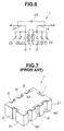
- An example of such a multilayer microelectronic circuit J is constructed in a structure shown in Figs. 7 and 8 to form an electrical circuit, in which an input line I', an output line O', grounding lines G' and signal lines NC' are formed at the side surfaces S1' of the multilayer microelectronic circuit.
- the input line I' is connected with an input section of the electrical circuit.
- the output line O' is connected with an output section of the electrical circuit.
- the grounding lines G' is connected with a grounding section of the electrical circuit.
- the signal line NC' is formed to connect various sections of the electrical circuit.
- This multilayer microelectronic circuit is directly mounted at its mounting surface (or lower surface) S2' on the surface of an electrical substrate K as shown in Fig. 8 where the upper surface S3' is observed.
- the mounting surface (or the lower surface) is shown in Fig. 7.
- the input line I' is connected with a patterned signal input contact Ib' of the substrate K.
- the output line O' is connected with a patterned signal output contact Ob' of the substrate K.
- the grounding lines G' are connected with a patterned grounding contact Gb' of the substrate K.
- Each signal line NC' is adapted to connect the various sections of the electrical circuit formed inside the multilayer microelectronic circuit and therefore is required to be disconnected from the various patterned wiring of the substrate K. Accordingly, the substrate is formed on its surface with a section a to which the signal line is electrically connected, and a generally circular insulating section ⁇ for insulating the section ⁇ from electrical contact with other sections such as the patterned grounding contact Gb'.
- Another object of the present invention is to provide an improved multilayer microelectronic circuit which is excellent in serviceableness while making it unnecessary to accomplish a process for forming an insulating section on the surface of a substrate on which the circuit is directly mounted.
- a further object of the present invention is to provide an improved multilayer microelectronic circuit which has signal lines for electrically connecting various sections of an electrical circuit, in which each line is formed in a disconnected state relative to a patterned wiring of a substrate on which the multilayer microelectronic circuit is directly mounted.
- An aspect of the present invention resides in a multilayer microelectronic circuit which is to be directly mounted on a substrate and comprises a plurality of dielectric layers and patterned electrodes which are laminated one upon another to form a laminated structure, the dielectric layers and the patterned electrodes forming an electrical circuit.
- the laminated structure has side surfaces extending along a direction in which the dielectric layers and the patterned electrodes are laminated.
- An input line is formed at one of the side surfaces and connected with an input section of the electrical circuit.
- An output line is formed at one of the side surfaces and connected with an output section of the electrical circuit.
- a grounding line formed at one of the side surfaces and connected with a grounding section of the electrical circuit Additionally, a signal line formed at one of the side surfaces, for connecting sections of the electrical circuit.
- the signal line has an end positioned adjacent a mounting surface at which the multilayer microelectronic circuit is directly mounted on the substrate, in which the end of the signal line is separate from the mounting surface so as to be insulated from electrical contact with the substrate.
- Another aspect of the present invention resides a multilayer microelectronic circuit which is to be directly mounted on a substrate and comprises a plurality of dielectric layers and patterned electrodes which are laminated one upon another to form a laminated structure.
- the dielectric layers and said patterned electrodes form an electrical circuit.
- the laminated structure has side surfaces extending along a direction in which said dielectric layers and said patterned electrodes are laminated.
- the dielectric layers includes a lower-most dielectric layer which has a mounting surface at which said multilayer microelectronic circuit is directly mounted on the substrate.
- the dielectric layers other than said lower-most dielectric layer are formed respectively with grooves which form a channel at one of the side surfaces.
- the lower-most dielectric layer is free of said groove.
- An input line is formed at one of said side surfaces and connected with an input section of said electrical circuit.
- An output line is formed at one of said side surfaces and connected with an output section of said electrical circuit.
- a grounding line is formed at one of said side surfaces and connected with a grounding section of said electrical circuit.
- a signal line is formed at the surface of said channel, for connecting sections of said electrical circuit. The signal line has an end positioned adjacent said mounting surface. The end of said signal line is separate from said mounting surface so as to be insulated from electrical contact with the substrate.
- the signal line is formed in a disconnected state at their lower end formed at the side surface of the multilayer microelectronic circuit, thereby overcoming the conventional drawbacks in which the signal line is brought into connection with a patterned wiring of the substrate even though the multilayer microelectronic circuit is directly mounted on the substrate.
- the disconnected state of the signal line is accomplished by forming no channel in the lower-most dielectric layer to be in direct contact with the substrate. Accordingly, obtaining the disconnected state of the signal line can be largely facilitated thereby lowering the production cost of the multilayer microelectronic circuit.
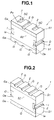
- the multilayer microelectronic circuit of this embodiment is constructed as a resonator.
- the resonator 1 comprises eight dielectric (insulating) layers Z1 to Z8 each of which is formed from a green sheet of a dielectric ceramic material as shown in Fig. 5.
- First to seventh patterned electrodes P1 to P7 are respectively formed on the upper surfaces of the second to eighth dielectric layers Z2 to Z8 other than that of the upper-most or first dielectric layer Z1, by screen-printing an electrically conductive paste.
- the dielectric layers Z1 to Z8 in the state of the green sheet are placed one upon another so that each of the patterned electrodes P1 to P7 is held between adjacent two of the dielectric layers Z1 to Z8, thus forming a green or laminated structure of the resonator 1. Then, the green structure of the resonator 1 is baked or sintered thereby forming the resonator 1 as shown in Figs. 1 to 4.
- Each of the dielectric layers Z1 to Z8 is formed at its peripheral surface with grooves (no numerals) which extend in the direction of thickness thereof, in the state of the green sheet.
- the grooves of the respective dielectric layers are connected with each other to form a channel 2 which is formed at the side surfaces S1 of the resonator 1 and extend in the direction of thickness of the resonator 1, in the state of the green structure of the resonator 1 in which the respective dielectric layers Z1 to Z8 are laminated.
- the surface of each channel 2 is metallized to form grounding lines G, an input line I, an output fine O, signal lines NC, as shown in Figs. 1 to 4.
- the lines G, I, O, NC may be formed by applying the electrically conductive paste at the surfaces of the channels of the green structure and then by baking the electrically conductive paste.
- the resonator 1 has an equivalent circuit shown in Fig. 6.
- the equivalent circuit includes two resonant inductors L, two resonant capacitors C1, two rough adjustment capacitors C2, two fine adjustment capacitors C3 two input/output capacitors C4, and a polarizing capacitor C5 through which input and output terminals are connected.
- Each of the inductors and each of the capacitors are constituted of some of the first to seventh patterned electrodes P1 to P7. More specifically, each resonant capacitor C1 is constituted of the fourth dielectric layer Z4 and the third and fourth patterned electrodes P3, P4 which are located on the upper- and lower surfaces of the fourth dielectric layer Z4.
- Each rough adjustment capacitor C2 is constituted of the third dielectric layer Z3 and the second and third patterned electrodes P2, P3 which are located at the upper and lower surfaces of the third dielectric layer Z3.
- Each fine adjustment capacitor C3 is constituted of the second dielectric layer Z2 and the first and second patterned electrodes P1, P2 located respectively at the upper- and lower surfaces of the second dielectric layer Z2.
- Each input/output capacitor C4 is constituted of the fifth dielectric layer Z5 and the fourth and fifth patterned electrodes P4, P5 located respectively at the upper and lower surfaces of the fifth dielectric layer Z5.
- each resonant inductor L is constituted of the seventh patterned electrode P7 located at the upper surface of the eighth dielectric layer Z8.
- the resonator 1 of this embodiment is adjusted in its resonant frequency by the following technique:
- the second patterned electrode P2 having a large area is subjected to trimming by using a laser cutting device (not shown) so as to roughly adjust the capacitance (for setting the resonant frequency) of the resonator 1.
- the first patterned electrode P1 having a small area is subjected to trimming by using the laser cutting device so as to finely adjust the capacitance of the resonator.
- the resonator 1 of this embodiment is used upon being directly put or mounted on a substrate 3 as shown in Fig. 4.
- the resonator 1 is provided at its lower (back-side) surface or mounting surface S2 (at which the resonator 1 is directly mounted on the substrate 3) with a patterned grounding contact Ga, a patterned input contact Ia, and a patterned output contact Oa as shown in Figs. 1 and 2.
- the patterned grounding contact Ga is connected with the patterned grounding lines G, so that the patterned grounding line G is brought into connection with a patterned grounding contact Gb formed at the surface of the substrate 3, in a state where the resonator 1 is directly mounted on the substrate 3.
- the input line I is adapted to connect one of two sections of the fifth patterned electrode P5 with the patterned input contact Ia, so that the input line I is brought into connection with the patterned input contact Ib of the substrate 3 in the state where the resonator 1 is directly mounted on the substrate as shown in Fig. 4.
- the output line O is adapted to connect the other of the two sections of the fifth patterned electrode P5 with the patterned output contact Oa, so that the output line O is brought into connection with the patterned output contact Ob of the substrate 3 in the state where the resonator I is directly mounted on the substrate as shown in Fig. 4. It will be understood that the patterned input and output contacts Ib, Ob are formed at the surface of the substrate 3.
- the signal lines NC are adapted to connect the second, fourth, and seventh patterned electrodes P2, P4, P7 with each other, so that the signal lines are separate and insulated from electrical contact with the substrate 3 in a state where the resonator 1 is directly mounted on the substrate 3 as shown in Fig. 4.
- each of the signal lines NC has a lower end separate from the lower surface or mounting surface S2 (at which the resonator 1 is directly mounted on the substrate 3) of the resonator 1.
- each signal line NC is kept in a disconnected state at its lower end. This state of each signal line NC is accomplished by avoiding formation of the groove at the peripheral surface of the eighth or lower-most dielectric layer Z8, the groove forming part of each channel 2 serving as the signal line NC.
- each signal line NC is insulated from electrical contact with the patterned grounding contact Gb of the substrate 3. It will be understood that the above-mentioned lower surface S2 of the resonator 1 is parallel with the upper surface S3 and generally perpendicular to the side surfaces S1.
- the signal lines NC of the resonator 1 are formed in the disconnected state at their lower end formed at the side surface of the resonator 1, thereby overcoming the problem of the signal lines NC being brought into connection with the patterned grounding contacts Gb even though the resonator 1 is directly mounted on the substrate 3 as shown in Fig. 4.
- the disconnected state of the signal lines NC is accomplished by forming no channel (2) at the portion Ps of the eighth dielectric layer Z8 contiguous with each signal line NC. Accordingly, obtaining the disconnected state of the signal lines NC can be largely facilitated thereby lowering the production cost of the resonator 1.
- the disconnected state of the signal lines NC has been shown and described as being accomplished by forming no channel at the portion (of the dielectric layer) contiguous with each signal line in the above embodiment, it will be understood that the disconnected state may be formed by other means, for example, first by forming each signal line NC to extend to the lower surface of the resonator (like in the conventional resonator) and then by trimming or cutting an end section of the thus formed signal line NC which end section reaches the lower surface.
Landscapes
- Engineering & Computer Science (AREA)
- Microelectronics & Electronic Packaging (AREA)
- Production Of Multi-Layered Print Wiring Board (AREA)
- Fixed Capacitors And Capacitor Manufacturing Machines (AREA)
- Structures For Mounting Electric Components On Printed Circuit Boards (AREA)
- Control Of Motors That Do Not Use Commutators (AREA)
- Filters And Equalizers (AREA)
Applications Claiming Priority (3)
| Application Number | Priority Date | Filing Date | Title |
|---|---|---|---|
| JP42750/97 | 1997-02-26 | ||
| JP4275097 | 1997-02-26 | ||
| JP9042750A JPH10241996A (ja) | 1997-02-26 | 1997-02-26 | 積層回路 |
Publications (2)
| Publication Number | Publication Date |
|---|---|
| EP0862238A2 true EP0862238A2 (fr) | 1998-09-02 |
| EP0862238A3 EP0862238A3 (fr) | 1999-06-23 |
Family
ID=12644690
Family Applications (1)
| Application Number | Title | Priority Date | Filing Date |
|---|---|---|---|
| EP98103314A Withdrawn EP0862238A3 (fr) | 1997-02-26 | 1998-02-25 | Circuit multi-couche microélectronique |
Country Status (4)
| Country | Link |
|---|---|
| US (1) | US6046409A (fr) |
| EP (1) | EP0862238A3 (fr) |
| JP (1) | JPH10241996A (fr) |
| CA (1) | CA2228316A1 (fr) |
Cited By (1)
| Publication number | Priority date | Publication date | Assignee | Title |
|---|---|---|---|---|
| EP1263038A3 (fr) * | 2001-05-31 | 2005-03-30 | Ngk Spark Plug Co., Ltd | Composant électronique et dispositif mobile de communication utilisant un tel composant électronique |
Families Citing this family (32)
| Publication number | Priority date | Publication date | Assignee | Title |
|---|---|---|---|---|
| TW535352B (en) * | 2000-05-30 | 2003-06-01 | Alps Electric Co Ltd | Surface-mounting type electronic circuit unit |
| FI20001384A7 (fi) * | 2000-06-09 | 2001-12-10 | Nokia Corp | Upotetun rakenteen virittäminen |
| JP2002141248A (ja) * | 2000-11-02 | 2002-05-17 | Murata Mfg Co Ltd | セラミック電子部品およびその製造方法 |
| JP4171218B2 (ja) * | 2002-01-23 | 2008-10-22 | 三菱電機株式会社 | 表面実装モジュール |
| US8928602B1 (en) | 2009-03-03 | 2015-01-06 | MCube Inc. | Methods and apparatus for object tracking on a hand-held device |
| US8486723B1 (en) | 2010-08-19 | 2013-07-16 | MCube Inc. | Three axis magnetic sensor device and method |
| US8797279B2 (en) | 2010-05-25 | 2014-08-05 | MCube Inc. | Analog touchscreen methods and apparatus |
| US8553389B1 (en) | 2010-08-19 | 2013-10-08 | MCube Inc. | Anchor design and method for MEMS transducer apparatuses |
| US8823007B2 (en) | 2009-10-28 | 2014-09-02 | MCube Inc. | Integrated system on chip using multiple MEMS and CMOS devices |
| US8477473B1 (en) | 2010-08-19 | 2013-07-02 | MCube Inc. | Transducer structure and method for MEMS devices |
| US8476129B1 (en) | 2010-05-24 | 2013-07-02 | MCube Inc. | Method and structure of sensors and MEMS devices using vertical mounting with interconnections |
| US8421082B1 (en) | 2010-01-19 | 2013-04-16 | Mcube, Inc. | Integrated CMOS and MEMS with air dielectric method and system |
| US8395252B1 (en) | 2009-11-13 | 2013-03-12 | MCube Inc. | Integrated MEMS and CMOS package and method |
| US8710597B1 (en) | 2010-04-21 | 2014-04-29 | MCube Inc. | Method and structure for adding mass with stress isolation to MEMS structures |
| US9709509B1 (en) | 2009-11-13 | 2017-07-18 | MCube Inc. | System configured for integrated communication, MEMS, Processor, and applications using a foundry compatible semiconductor process |
| US8637943B1 (en) | 2010-01-04 | 2014-01-28 | MCube Inc. | Multi-axis integrated MEMS devices with CMOS circuits and method therefor |
| US8936959B1 (en) | 2010-02-27 | 2015-01-20 | MCube Inc. | Integrated rf MEMS, control systems and methods |
| US8794065B1 (en) | 2010-02-27 | 2014-08-05 | MCube Inc. | Integrated inertial sensing apparatus using MEMS and quartz configured on crystallographic planes |
| US8367522B1 (en) * | 2010-04-08 | 2013-02-05 | MCube Inc. | Method and structure of integrated micro electro-mechanical systems and electronic devices using edge bond pads |
| US8928696B1 (en) | 2010-05-25 | 2015-01-06 | MCube Inc. | Methods and apparatus for operating hysteresis on a hand held device |
| US8869616B1 (en) | 2010-06-18 | 2014-10-28 | MCube Inc. | Method and structure of an inertial sensor using tilt conversion |
| US8652961B1 (en) | 2010-06-18 | 2014-02-18 | MCube Inc. | Methods and structure for adapting MEMS structures to form electrical interconnections for integrated circuits |
| US8993362B1 (en) | 2010-07-23 | 2015-03-31 | MCube Inc. | Oxide retainer method for MEMS devices |
| US8723986B1 (en) | 2010-11-04 | 2014-05-13 | MCube Inc. | Methods and apparatus for initiating image capture on a hand-held device |
| JP6006474B2 (ja) * | 2011-04-25 | 2016-10-12 | 日本特殊陶業株式会社 | 配線基板、多数個取り配線基板、およびその製造方法 |
| US8969101B1 (en) | 2011-08-17 | 2015-03-03 | MCube Inc. | Three axis magnetic sensor device and method using flex cables |
| USD680119S1 (en) * | 2011-11-15 | 2013-04-16 | Connectblue Ab | Module |
| USD689053S1 (en) * | 2011-11-15 | 2013-09-03 | Connectblue Ab | Module |
| USD692896S1 (en) * | 2011-11-15 | 2013-11-05 | Connectblue Ab | Module |
| USD668658S1 (en) * | 2011-11-15 | 2012-10-09 | Connectblue Ab | Module |
| USD680545S1 (en) * | 2011-11-15 | 2013-04-23 | Connectblue Ab | Module |
| USD668659S1 (en) * | 2011-11-15 | 2012-10-09 | Connectblue Ab | Module |
Family Cites Families (7)
| Publication number | Priority date | Publication date | Assignee | Title |
|---|---|---|---|---|
| US3349480A (en) * | 1962-11-09 | 1967-10-31 | Ibm | Method of forming through hole conductor lines |
| US4821007A (en) * | 1987-02-06 | 1989-04-11 | Tektronix, Inc. | Strip line circuit component and method of manufacture |
| JPH02306709A (ja) * | 1989-05-22 | 1990-12-20 | Murata Mfg Co Ltd | 電子部品の製造方法 |
| JP3058898B2 (ja) * | 1990-09-03 | 2000-07-04 | 三菱電機株式会社 | 半導体装置及びその評価方法 |
| US5404118A (en) * | 1992-07-27 | 1995-04-04 | Murata Manufacturing Co., Ltd. | Band pass filter with resonator having spiral electrodes formed of coil electrodes on plurality of dielectric layers |
| DE69411973T2 (de) * | 1993-03-25 | 1998-12-10 | Matsushita Electric Industrial Co., Ltd., Kadoma, Osaka | Geschichteter dielektrischer Resonator und dielektrisches Filter |
| JPH07193403A (ja) * | 1993-12-24 | 1995-07-28 | Murata Mfg Co Ltd | 共振器 |
-
1997
- 1997-02-26 JP JP9042750A patent/JPH10241996A/ja active Pending
-
1998
- 1998-02-25 EP EP98103314A patent/EP0862238A3/fr not_active Withdrawn
- 1998-02-25 CA CA002228316A patent/CA2228316A1/fr not_active Abandoned
- 1998-02-26 US US09/031,074 patent/US6046409A/en not_active Expired - Fee Related
Cited By (1)
| Publication number | Priority date | Publication date | Assignee | Title |
|---|---|---|---|---|
| EP1263038A3 (fr) * | 2001-05-31 | 2005-03-30 | Ngk Spark Plug Co., Ltd | Composant électronique et dispositif mobile de communication utilisant un tel composant électronique |
Also Published As
| Publication number | Publication date |
|---|---|
| US6046409A (en) | 2000-04-04 |
| JPH10241996A (ja) | 1998-09-11 |
| EP0862238A3 (fr) | 1999-06-23 |
| CA2228316A1 (fr) | 1998-08-26 |
Similar Documents
| Publication | Publication Date | Title |
|---|---|---|
| US6046409A (en) | Multilayer microelectronic circuit | |
| US7085124B2 (en) | Multilayer capacitor | |
| US6310525B1 (en) | Dielectric laminated device and its manufacturing method | |
| US7209362B2 (en) | Multilayer ceramic substrate with a cavity | |
| JPH07193403A (ja) | 共振器 | |
| US5239280A (en) | Dielectric filter having inductive input/output coupling | |
| JP2001230610A (ja) | 積層型誘電体共振器 | |
| EP0635897B1 (fr) | Filtre diélectrique | |
| JPH0191502A (ja) | 誘電体共振器 | |
| US6924707B2 (en) | Resonator | |
| JP3259738B2 (ja) | トランスバーサルフィルタ | |
| JP2710904B2 (ja) | 積層型誘電体フィルタ | |
| JP2661004B2 (ja) | 誘電体フィルタ | |
| JP2004296927A (ja) | 電子部品収納用配線基板 | |
| JPH05191103A (ja) | 積層型誘電体フィルタ | |
| JPH11150402A (ja) | 積層形フィルタ | |
| CA2293131A1 (fr) | Filtre planaire | |
| JP2598341Y2 (ja) | 積層型誘電体ストリップライン共振器 | |
| JP2001016009A (ja) | ストリップライン共振器 | |
| JP2002198703A (ja) | 積層型誘電体フィルタ | |
| JP2004260377A (ja) | バラントランス | |
| JP2000022480A (ja) | 積層型フィルタ | |
| JP2004187222A (ja) | 誘電体フィルタ | |
| JPH10276018A (ja) | 誘電体共振器及び誘電体フィルタの製造方法 | |
| JPH06291508A (ja) | 高周波フィルタ |
Legal Events
| Date | Code | Title | Description |
|---|---|---|---|
| PUAI | Public reference made under article 153(3) epc to a published international application that has entered the european phase |
Free format text: ORIGINAL CODE: 0009012 |
|
| AK | Designated contracting states |
Kind code of ref document: A2 Designated state(s): DE GB |
|
| AX | Request for extension of the european patent |
Free format text: AL;LT;LV;MK;RO;SI |
|
| PUAL | Search report despatched |
Free format text: ORIGINAL CODE: 0009013 |
|
| AK | Designated contracting states |
Kind code of ref document: A3 Designated state(s): AT BE CH DE DK ES FI FR GB GR IE IT LI LU MC NL PT SE |
|
| AX | Request for extension of the european patent |
Free format text: AL;LT;LV;MK;RO;SI |
|
| RIC1 | Information provided on ipc code assigned before grant |
Free format text: 6H 01P 7/08 A, 6H 01P 1/203 B |
|
| 17P | Request for examination filed |
Effective date: 19990716 |
|
| AKX | Designation fees paid |
Free format text: DE GB |
|
| 17Q | First examination report despatched |
Effective date: 20030728 |
|
| STAA | Information on the status of an ep patent application or granted ep patent |
Free format text: STATUS: THE APPLICATION IS DEEMED TO BE WITHDRAWN |
|
| 18D | Application deemed to be withdrawn |
Effective date: 20031208 |