EP0871211A2 - Procédé de traitement par plasma et procédé de fabrication d'un composant semiconducteur - Google Patents
Procédé de traitement par plasma et procédé de fabrication d'un composant semiconducteur Download PDFInfo
- Publication number
- EP0871211A2 EP0871211A2 EP98302036A EP98302036A EP0871211A2 EP 0871211 A2 EP0871211 A2 EP 0871211A2 EP 98302036 A EP98302036 A EP 98302036A EP 98302036 A EP98302036 A EP 98302036A EP 0871211 A2 EP0871211 A2 EP 0871211A2
- Authority
- EP
- European Patent Office
- Prior art keywords
- etching
- cleaning
- gas
- plasma
- dry cleaning
- Prior art date
- Legal status (The legal status is an assumption and is not a legal conclusion. Google has not performed a legal analysis and makes no representation as to the accuracy of the status listed.)
- Withdrawn
Links
Images


Classifications
-
- H—ELECTRICITY
- H01—ELECTRIC ELEMENTS
- H01J—ELECTRIC DISCHARGE TUBES OR DISCHARGE LAMPS
- H01J37/00—Discharge tubes with provision for introducing objects or material to be exposed to the discharge, e.g. for the purpose of examination or processing thereof
- H01J37/32—Gas-filled discharge tubes
- H01J37/32431—Constructional details of the reactor
- H01J37/32798—Further details of plasma apparatus not provided for in groups H01J37/3244 - H01J37/32788; special provisions for cleaning or maintenance of the apparatus
- H01J37/32853—Hygiene
- H01J37/32862—In situ cleaning of vessels and/or internal parts
-
- H—ELECTRICITY
- H10—SEMICONDUCTOR DEVICES; ELECTRIC SOLID-STATE DEVICES NOT OTHERWISE PROVIDED FOR
- H10P—GENERIC PROCESSES OR APPARATUS FOR THE MANUFACTURE OR TREATMENT OF DEVICES COVERED BY CLASS H10
- H10P70/00—Cleaning of wafers, substrates or parts of devices
- H10P70/10—Cleaning before device manufacture, i.e. Begin-Of-Line process
- H10P70/12—Cleaning before device manufacture, i.e. Begin-Of-Line process by dry cleaning only
-
- C—CHEMISTRY; METALLURGY
- C23—COATING METALLIC MATERIAL; COATING MATERIAL WITH METALLIC MATERIAL; CHEMICAL SURFACE TREATMENT; DIFFUSION TREATMENT OF METALLIC MATERIAL; COATING BY VACUUM EVAPORATION, BY SPUTTERING, BY ION IMPLANTATION OR BY CHEMICAL VAPOUR DEPOSITION, IN GENERAL; INHIBITING CORROSION OF METALLIC MATERIAL OR INCRUSTATION IN GENERAL
- C23C—COATING METALLIC MATERIAL; COATING MATERIAL WITH METALLIC MATERIAL; SURFACE TREATMENT OF METALLIC MATERIAL BY DIFFUSION INTO THE SURFACE, BY CHEMICAL CONVERSION OR SUBSTITUTION; COATING BY VACUUM EVAPORATION, BY SPUTTERING, BY ION IMPLANTATION OR BY CHEMICAL VAPOUR DEPOSITION, IN GENERAL
- C23C16/00—Chemical coating by decomposition of gaseous compounds, without leaving reaction products of surface material in the coating, i.e. chemical vapour deposition [CVD] processes
- C23C16/44—Chemical coating by decomposition of gaseous compounds, without leaving reaction products of surface material in the coating, i.e. chemical vapour deposition [CVD] processes characterised by the method of coating
- C23C16/4401—Means for minimising impurities, e.g. dust, moisture or residual gas, in the reaction chamber
- C23C16/4405—Cleaning of reactor or parts inside the reactor by using reactive gases
-
- H—ELECTRICITY
- H10—SEMICONDUCTOR DEVICES; ELECTRIC SOLID-STATE DEVICES NOT OTHERWISE PROVIDED FOR
- H10P—GENERIC PROCESSES OR APPARATUS FOR THE MANUFACTURE OR TREATMENT OF DEVICES COVERED BY CLASS H10
- H10P50/00—Etching of wafers, substrates or parts of devices
- H10P50/20—Dry etching; Plasma etching; Reactive-ion etching
- H10P50/24—Dry etching; Plasma etching; Reactive-ion etching of semiconductor materials
- H10P50/242—Dry etching; Plasma etching; Reactive-ion etching of semiconductor materials of Group IV materials
-
- H—ELECTRICITY
- H10—SEMICONDUCTOR DEVICES; ELECTRIC SOLID-STATE DEVICES NOT OTHERWISE PROVIDED FOR
- H10P—GENERIC PROCESSES OR APPARATUS FOR THE MANUFACTURE OR TREATMENT OF DEVICES COVERED BY CLASS H10
- H10P50/00—Etching of wafers, substrates or parts of devices
- H10P50/60—Wet etching
- H10P50/64—Wet etching of semiconductor materials
- H10P50/642—Chemical etching
-
- Y—GENERAL TAGGING OF NEW TECHNOLOGICAL DEVELOPMENTS; GENERAL TAGGING OF CROSS-SECTIONAL TECHNOLOGIES SPANNING OVER SEVERAL SECTIONS OF THE IPC; TECHNICAL SUBJECTS COVERED BY FORMER USPC CROSS-REFERENCE ART COLLECTIONS [XRACs] AND DIGESTS
- Y10—TECHNICAL SUBJECTS COVERED BY FORMER USPC
- Y10S—TECHNICAL SUBJECTS COVERED BY FORMER USPC CROSS-REFERENCE ART COLLECTIONS [XRACs] AND DIGESTS
- Y10S438/00—Semiconductor device manufacturing: process
- Y10S438/905—Cleaning of reaction chamber
Definitions
- the present invention relates a method for dry-cleaning the interior of semiconductor manufacturing apparatus for use in performing microfabrication or film formation on substrates during the manufacturing processes of semiconductor devices.
- the invention also relates to a method for manufacturing semiconductor devices by use of semiconductor manufacturing apparatus with its inside cleaned.
- some processes are becoming more important, including dry etching technology using plasma, chemical vapor deposition (CVD) and the like. More specifically, the processes are to perform microfabrication such as film formation, etching and the like by utilizing plasma reaction of various kinds of gases as introduced into the apparatus.
- deposition films tend to be left adhered also to the inner walls of manufacturing apparatus used, other than a target substrate being subjected to such microfabrication.
- certain deposition films can be adhered to the inner walls of the apparatus due to decomposition or combination of etching gases within a plasma and also due to generation of secondary etching products during etching.
- one typical approach to removal of such adhesion deposits is the so-called wet cleaning technology-i.e. wiping out them by using catalytic substance such as alcohol or pure water or the like while letting the apparatus be exposed to the atmosphere.
- Another prior known approach is a dry cleaning scheme using a combination of chlorine-based gas and fluorine-based gas as disclosed, for example, in Published Unexamined Japanese Patent Application (PUJPA) No. 3-62520.
- a further prior art approach is a dry cleaning technique using a plasma of a mixture of oxygen gas and chlorine gas as disclosed for example in PUJPA No. 7-508313.
- the material to be etched is an alloy containing therein Al and W, and therefore the technique disclosed therein is featured in that the cleaning steps for a plurality of etching objects are combined together in order to remove away Al's etching products as well as W's etching products.
- the third prior art approach employing the dry cleaning technique as taught by PUJPA No. 7-508313 is featured by removing what is called the reaction products as originated from chemical reaction between the to-be-etched material and an etching gas used or between a photoresist (carbon) employed as a mask layer material for etching and the etching gas or still alternatively due to polymeric bodies of the etching gas.
- etching apparatus a plasma created by the etching gas attempts to etch the substrate surface to be etched and simultaneously sputter the apparatus internal member materials also, which might result in attachment and adhesion of certain materials onto the inner walls of the apparatus, which materials may include in addition to etching reaction products either ion-sputtered matter of such apparatus internal member materials or chemical compounds of the apparatus internal member materials and of the etching gas employed.
- the prior art dry cleaning methodology is faced with a serious problem left unsolved: it is not possible to fully remove away the ion sputtered matter or products of the apparatus internal member materials or the chemical compounds of such apparatus materials and etching gas, which results in generation of contaminants due to lamination of resultant non-removed materials left on the inner walls of the apparatus.
- the invention provides a specific dry etching process which includes the steps of removing etching reaction products, and removing either ion sputtered constituents of those materials of the internal structure members of manufacturing apparatus or chemical compounds of such apparatus materials and an etching gas used.
- the invention also provides a dry cleaning process which makes use of a chosen gas that contains therein a material having its interatomic bonding energy with respect to elements constituting a gas for use during an etching and a cleaning step, which energy is greater in value than the atomic bonding energy between elements constituting a material to be etched and elements constituting a gas or gases used during the etching and cleaning processes.
- the invention further consists in employing for the dry cleaning process a specific kind of gas which contains therein a material that has its interatomic bonding energy with respect to elements constituting gases for use in the etching and cleaning steps, which energy is greater in value than the interatomic bonding energy between elements constituting the apparatus internal member materials and those elements constituting gases used in the etching and cleaning processes.
- Fig. 1 is a diagram showing semiconductor manufacturing apparatus incorporating the principles of the present invention.
- Fig. 2A and 2B are diagrams illustrating, in cross-section, two major steps in the manufacture of a semiconductor wafer in accordance with a first embodiment of the invention.
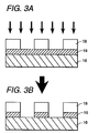
- Fig. 3A and 3B are diagrams depicting in cross-section two major steps in the manufacture of a semiconductor wafer in accordance with a second embodiment of the invention.
- Fig. 4A and 4B are diagrams showing in cross-section two major steps in the manufacture of a semiconductor wafer in accordance with a third embodiment of the invention.
- Fig. 1 illustrates a configuration of microwave etching apparatus adapted for use in performing the dry cleaning method in accordance with the present invention.
- reference numeral 1 designates a silicon wafer (substrate) to be subjected to microfabrication; numerals 3 and 4 denote a quartz bell jar and a main chamber for establishment of the vacuum environment required.
- 10 indicates an exhaust port for vacuum evacuation whereas 15 denotes a gas introduction section for introduction of a gas or gases used in etching or dry cleaning.
- 9 is a substrate stage for rigid support of a wafer under manufacture; 8 is a clamper for clamping the wafer. This clamper may typically be made of ceramics including, but not limited to, alumina ceramics.
- Electrostatic suction force may be used to rigidly support the wafer on the substrate stage 9.
- 7 designates an Earth plate; 11 denotes a high-frequency power supply for application of a radiofrequency (RF) bias voltage between the Earth plate 7 and wafer stage 9.
- RF radiofrequency
- the microwave etching apparatus shown herein is first subject to introduction of a chosen gas for use in generating a plasma after completion of high vacuum evacuation. Then, microwaves 14 are excited by a magnetron (not shown) and are then introduced via the waveguide 5 into the quartz bell jar 3 (processing room) causing a gas in the processing room to transform into a plasma by electronic cyclotron resonance (ECR) with a magnetic field as created by the solenoid 6 disposed around the processing room, which plasma is used to effectuate an intended etching treatment.
- ECR electronic cyclotron resonance
- the RF bias voltage is applied by the high-frequency power supply 11 between the Earth plate 7 and wafer stage 9 for the purpose of performing an anisotropic etching by attraction of ions thereto.
- a silicon oxide film (SiO 2 ) 17 for use as a dielectric film shown in Fig. 2 (Fig. 2A and 2B) is etched using a plasma of fluorocarbon-based gas-here, CF 4 gas-and plasma of additive gases of Ar and O 2 .
- the SiO 2 film 17 is formed on a substrate 16 by way of example, and a mask pattern 18 made of a chosen photoresist material is further formed thereon allowing the resulting structure to be subject to an etching treatment by use of the etching apparatus shown in Fig. 1.
- the etching gas attempts to dissociate in the plasma hitting the target wafer so that the etching progresses accordingly.
- any unnecessary deposits left adhered to the inner walls of the apparatus with the to-be-etched object being as the cause thereof may become oxides containing silicon and chemical compounds containing organic substance.
- a gas used for dry cleaning is aimed at creation of chemical compounds of increased vapor pressure by reaction with the deposits to be removed away, which will finally be removed through vaporization and vacuum evacuation.
- a plasma of O 2 gas is applied thereto permitting vaporization thereof to CO or CO 2 gases for removal.
- the prior art approach as taught by PUJPA No. 7-508313 indicated in the introductory part of the description is designed to employ a cleaning gas consisting of the mixture of a chlorine-based gas and oxygen-based gas. Mixing oxygen thereinto may improve the efficiency as a whole by disconnecting or separating carbon from chemical compounds containing therein metal and chlorine as well as organic substance while cleaning the metal by chlorine.
- cleaning is typically done using a mixture or combination of a fluorine-based gas and oxygen-based gas.
- the plasma originated from the etching gas attempts, in addition to etching the substrate surfaces 17, 18 to be etched, to hit also the materials of apparatus internal parts or components such as for example the clamper 8 and Earth plate 7 resulting in an increase in amount of undesired secondary etching products devotable to creation of the deposition film 13, which products may include in addition to the reaction products of the to-be-etched material either the ion sputtered products of the apparatus internal component materials or chemical compounds of such apparatus materials and of the etching gas used herein.
- alumina components are employed in plasma-applied semiconductor manufacturing apparatus including the etching apparatus.
- unnecessary deposits stacked or adhered to the apparatus inner walls may be left in the form of organic compounds of the to-be-etched SiO 2 material and of resist material which are originated from the to-be-etched object per se and also in the form of alumina as a result of ion sputtering due to the fact that the clamper 8 as one of the alumina components inside the apparatus is hit by a plasma. Part of this may be attached and adhered in the form of aluminum fluoride by reaction of fluorine during etching.
- the prior art dry cleaning architecture merely comes with a cleaning treatment with respect to limited materials such as SiO 2 and organic compounds of resist materials.
- the prior art fails to take into consideration in any way the depositability of either sputtered products of the apparatus internal component materials or chemical compounds of such apparatus materials and etching gas; obviously, the prior art does not take account of how a cleaning is to be done therefor. Accordingly, these might be finally left as the cause for generation of contaminants.
- the present invention it becomes possible, by adding to the dry etching process both the step of removing etching reaction products and the step of removing any chemical compounds of the apparatus inside component materials and etching gas(es), to successfully remove away also the deposits made of such compounds of the apparatus internal component materials which have been long ignored in the conventional dry cleaning technology, which in turn leads to capability of improving the cleaning effect while simultaneously increasing the contaminant generation suppression effect.
- the illustrative embodiment is specifically designed to add as the apparatus inside material cleaning treatment a cleaning step using a mixture gas of BCl 3 and Cl 2 .
- Aluminum attachments may be effectively removed away by production of AlCl 3 of high vapor pressure using a Cl 2 gas plasma.
- Cl 2 gas plasma
- the plasma of Cl 2 alone is incapable of producing AlCl 3 rendering it impossible to effectuate any intended removal by cleaning due to the fact that the interatomic bonding energy of Al-O and Al-F remains greater than the interatomic bonding energy of Al-C.
- a specifically arranged gas containing therein B such as a BCl 3 gas, which has its interatomic bonding energy with respect to fluorine and oxygen as greater in value than the interatomic bonding energy of Al-O and Al-F, is mixed into the Cl 2 gas thereby removing O and F out of Al-O and Al-F to thereby render effective the cleaning by Cl 2 .
- This may in turn enable achievement of successful removal of ion sputtered products of the apparatus internal component materials along with removal of inherent etching reaction products.
- sequential execution of a cleaning using O 2 and sulphur hexafluoride (SF 6 ) and cleaning using a mixture gas of BCl 3 and Cl 2 may remarkably increase the cleaning effect inside the apparatus and also the contaminant suppression effect therein.
- the cleaning effect within the apparatus may dramatically be improved by performing the dry cleaning process for removal of ion sputtered products of the apparatus internal member materials or any chemical compounds of such apparatus materials and an etching gas in addition to the dry cleaning for removal of reactive products with respect to the to-be-etched material. While in this embodiment the dry cleaning for such etching reaction products and the cleaning with respect to the apparatus internal member materials are done sequentially, the two cleaning gases may alternatively be mixed together.
- a tungsten lead wire layer 19 is formed on the substrate 16 while a mask pattern 18 made of a chosen photoresistive material is formed thereon; the resulting structure is then subject to an etching process in the etching apparatus shown in Fig. 1.
- a plasma of SF 6 gas is used to facilitate progression of an etching required.
- any unnecessary deposits can be left adhered to the apparatus inner walls in the form of chemical compounds containing therein tungsten, fluorine and organic substance, and further aluminum oxide as ion-sputtered during the clamper 8 that is one of the alumina components inside the apparatus is being hit by a plasma.
- Part of this is in the form of aluminum fluoride due to the plasma of SF 6 gas during etching.
- both the cleaning using SF 6 and the cleaning using the mixture gas of BCl 3 and Cl 2 were done in a sequential manner.
- SF 6 may exhibit some cleaning effects with respect to tungsten and organic substance also.
- the cleaning using the BCl 3 /Cl 2 mixture gas exhibits cleaning effects with respect to aluminum oxide and aluminum fluoride as has been explained in conjunction with the first embodiment. This cleaning is advantageous in extremely improving the contaminant suppression effect.
- the cleaning effect may be noticeably enhanced by performing both the dry cleaning process for removal of reaction products with respect to the etching material and also the dry cleaning with respect to the apparatus internal member materials.
- etching a lamination film structure consisting essentially of an aluminum lead-wire layer 20 and titanium-tungsten (TiW) barrier metal 21. As stated previously, etching is performed in a way such that a chosen chemical compound of high vapor pressure relative to the material to be etched is formed letting the etching progress.
- the first layer 20 made of aluminum is etched by altering to AlCl 3 of high vapor pressure using a Cl 2 gas.
- Al or AlCl x can be attached and adhered for deposition to the apparatus inner walls, including several structure components of the processing room, such as for example the quartz bell jar 3, main chamber 4, gas introduction port 15, and clamper 8.
- the second layer of TiW 2 O is processed by a SF 6 plasma; at this time, Ti or tungsten (W) might be stacked and adhered to the apparatus inner walls and/or the constituent components of the processing room thereof.
- the Cl 2 plasma may be used for removal thereof by altering them to AlCl 3 and TiCl of higher vapor pressure.
- a plasma of fluoride gas such as for example SF 6 plasma, is employable to remove the same by altering it to WF 6 of higher vapor pressure.
- any possible additive deposits are such that:
- the plasma of etching gas and that of cleaning gas will possibly hit the apparatus inside materials also, which results in attachment of ion sputtered products of such apparatus materials to inside of the apparatus. These may also become chemical compounds with the etching gas and cleaning gas. These can raise a serious bar to achievement of an intended cleaning in both performance and reliability.
- the dry cleaning process is specifically added with a cleaning step using a specific gas containing therein a chosen material having the interatomic bonding energy with the etching gas elements which energy is greater in value than the interatomic energy between the element(s) constituting the to-be-etched object and those constituting the etching gas.
- Another advantage of the invention lies in capability of removing the deposits discussed supra at Paragraph 3) because of the fact that the step of removing ion sputtered products of the apparatus internal member materials is added along with the step of removing etching reaction products. This in turn makes it possible to remove any ion sputtered products of aluminum components used as internal parts or components of the etching apparatus employed.
- the dry cleaning process is specifically arranged to include a cleaning step using a specific gas containing therein a material having the interatomic bonding energy with the gas elements of the cleaning step, which energy is greater in value than the interatomic bonding energy between inherent materials, including the to-be-etched material and apparatus component materials, and the elements constituting the cleaning gases at other steps.
- This may advantageously serve to enable successful removal of those deposits of the kinds as discussed at Paragraphs 2) and 4) to 5). In other words, it becomes possible to remove any deposits which have become aluminum fluoride due to the SF 6 plasma during the W cleaning.
- B is such that the interatomic bonding energy of B-O is greater than that of aluminum oxide Al-O which is the ion sputtered products of the apparatus internal member material(s). Accordingly, mixing a B-contained gas and BCl 3 into Cl 2 gas enables separation of O from Al-O rendering more effective the cleaning by Cl 2 . This makes it possible to remove any ion sputtered products of the apparatus internal member materials also.
- the aforesaid cleaning process for certain the films deposited by reaction with the etching and cleaning gases at the next step as required due to the multilayer lamination film structure may be performed before and/or after the cleaning process for etching reaction products alone.
Landscapes
- Chemical & Material Sciences (AREA)
- Engineering & Computer Science (AREA)
- General Chemical & Material Sciences (AREA)
- Chemical Kinetics & Catalysis (AREA)
- Materials Engineering (AREA)
- Mechanical Engineering (AREA)
- Metallurgy (AREA)
- Organic Chemistry (AREA)
- Health & Medical Sciences (AREA)
- Epidemiology (AREA)
- Public Health (AREA)
- Physics & Mathematics (AREA)
- Plasma & Fusion (AREA)
- Analytical Chemistry (AREA)
- Drying Of Semiconductors (AREA)
- Cleaning Or Drying Semiconductors (AREA)
- ing And Chemical Polishing (AREA)
Applications Claiming Priority (3)
| Application Number | Priority Date | Filing Date | Title |
|---|---|---|---|
| JP66099/97 | 1997-03-19 | ||
| JP6609997 | 1997-03-19 | ||
| JP6609997A JP3594759B2 (ja) | 1997-03-19 | 1997-03-19 | プラズマ処理方法 |
Publications (2)
| Publication Number | Publication Date |
|---|---|
| EP0871211A2 true EP0871211A2 (fr) | 1998-10-14 |
| EP0871211A3 EP0871211A3 (fr) | 1999-12-08 |
Family
ID=13306104
Family Applications (1)
| Application Number | Title | Priority Date | Filing Date |
|---|---|---|---|
| EP98302036A Withdrawn EP0871211A3 (fr) | 1997-03-19 | 1998-03-18 | Procédé de traitement par plasma et procédé de fabrication d'un composant semiconducteur |
Country Status (7)
| Country | Link |
|---|---|
| US (1) | US6186153B1 (fr) |
| EP (1) | EP0871211A3 (fr) |
| JP (1) | JP3594759B2 (fr) |
| KR (1) | KR100531337B1 (fr) |
| CN (1) | CN1193812A (fr) |
| SG (1) | SG64481A1 (fr) |
| TW (1) | TW410398B (fr) |
Cited By (3)
| Publication number | Priority date | Publication date | Assignee | Title |
|---|---|---|---|---|
| WO2002067310A1 (fr) * | 2001-02-22 | 2002-08-29 | Sanko Co., Ltd. | Procede et dispositif de nettoyage d'elements en ceramique |
| EP1536035A3 (fr) * | 2003-11-25 | 2005-07-13 | Air Products And Chemicals, Inc. | Procédé de nettoyage d'une chambre de dépôt pour matériaux à constante diélectrique élevée |
| US8486198B2 (en) | 2005-08-04 | 2013-07-16 | Aviza Technology Limited | Method of processing substrates |
Families Citing this family (25)
| Publication number | Priority date | Publication date | Assignee | Title |
|---|---|---|---|---|
| JP2000272156A (ja) * | 1999-03-26 | 2000-10-03 | Fuji Photo Film Co Ltd | カーボン膜の成膜方法 |
| JP3838614B2 (ja) | 1999-11-10 | 2006-10-25 | 松下電器産業株式会社 | 半導体装置の製造方法 |
| KR100655217B1 (ko) * | 2000-06-27 | 2006-12-08 | 삼성전자주식회사 | 고주파 플라즈마 챔버의 세정 방법 |
| JP2002129334A (ja) * | 2000-10-26 | 2002-05-09 | Applied Materials Inc | 気相堆積装置のクリーニング方法及び気相堆積装置 |
| US6770214B2 (en) * | 2001-03-30 | 2004-08-03 | Lam Research Corporation | Method of reducing aluminum fluoride deposits in plasma etch reactor |
| JP3421329B2 (ja) * | 2001-06-08 | 2003-06-30 | 東京エレクトロン株式会社 | 薄膜形成装置の洗浄方法 |
| JP2003068705A (ja) * | 2001-08-23 | 2003-03-07 | Hitachi Ltd | 半導体素子の製造方法 |
| TW508648B (en) * | 2001-12-11 | 2002-11-01 | United Microelectronics Corp | Method of reducing the chamber particle level |
| US7326673B2 (en) * | 2001-12-31 | 2008-02-05 | Advanced Technology Materials, Inc. | Treatment of semiconductor substrates using long-chain organothiols or long-chain acetates |
| US7557073B2 (en) * | 2001-12-31 | 2009-07-07 | Advanced Technology Materials, Inc. | Non-fluoride containing supercritical fluid composition for removal of ion-implant photoresist |
| US20040011380A1 (en) * | 2002-07-18 | 2004-01-22 | Bing Ji | Method for etching high dielectric constant materials and for cleaning deposition chambers for high dielectric constant materials |
| JP4196371B2 (ja) * | 2002-08-20 | 2008-12-17 | キヤノンアネルバ株式会社 | ハロゲンガスの製造方法、ハロゲンガスの製造装置及びハロゲンガスの回収・循環システム |
| US6863930B2 (en) | 2002-09-06 | 2005-03-08 | Delphi Technologies, Inc. | Refractory metal mask and methods for coating an article and forming a sensor |
| US20050072444A1 (en) * | 2003-10-03 | 2005-04-07 | Shigeru Shirayone | Method for processing plasma processing apparatus |
| CN100352013C (zh) * | 2004-07-16 | 2007-11-28 | 鸿富锦精密工业(深圳)有限公司 | 干蚀刻后处理方法 |
| GB0516054D0 (en) * | 2005-08-04 | 2005-09-14 | Trikon Technologies Ltd | A method of processing substrates |
| JP5121698B2 (ja) * | 2006-03-06 | 2013-01-16 | 東京エレクトロン株式会社 | プラズマ処理装置 |
| JP4776575B2 (ja) * | 2007-03-28 | 2011-09-21 | 株式会社東芝 | 表面処理方法、エッチング処理方法および電子デバイスの製造方法 |
| JP5110987B2 (ja) * | 2007-07-05 | 2012-12-26 | 株式会社日立ハイテクノロジーズ | プラズマ処理方法およびコンピュータ読み取り可能な記録媒体 |
| JP2008078678A (ja) * | 2007-11-02 | 2008-04-03 | Hitachi Ltd | プラズマ処理方法 |
| US20100051577A1 (en) * | 2008-09-03 | 2010-03-04 | Micron Technology, Inc. | Copper layer processing |
| JP2012109472A (ja) | 2010-11-19 | 2012-06-07 | Hitachi High-Technologies Corp | プラズマ処理方法 |
| JP5736820B2 (ja) * | 2011-02-15 | 2015-06-17 | 富士通株式会社 | 半導体製造装置の洗浄装置及びそれを用いた半導体装置の製造方法 |
| JP2013030696A (ja) * | 2011-07-29 | 2013-02-07 | Ulvac Japan Ltd | プラズマエッチング装置、及びプラズマクリーニング方法 |
| JP6854600B2 (ja) * | 2016-07-15 | 2021-04-07 | 東京エレクトロン株式会社 | プラズマエッチング方法、プラズマエッチング装置、および基板載置台 |
Family Cites Families (18)
| Publication number | Priority date | Publication date | Assignee | Title |
|---|---|---|---|---|
| JPH0362550A (ja) * | 1989-07-31 | 1991-03-18 | Hitachi Ltd | 半導体集積回路 |
| JP2892694B2 (ja) * | 1989-07-31 | 1999-05-17 | 株式会社日立製作所 | プラズマクリーニング方法 |
| JPH0383335A (ja) * | 1989-08-28 | 1991-04-09 | Hitachi Ltd | エッチング方法 |
| JPH03130368A (ja) * | 1989-09-22 | 1991-06-04 | Applied Materials Inc | 半導体ウェーハプロセス装置の洗浄方法 |
| US5085727A (en) * | 1990-05-21 | 1992-02-04 | Applied Materials, Inc. | Plasma etch apparatus with conductive coating on inner metal surfaces of chamber to provide protection from chemical corrosion |
| US5108542A (en) * | 1990-08-23 | 1992-04-28 | Hewlett Packard Company | Selective etching method for tungsten and tungsten alloys |
| US5716494A (en) * | 1992-06-22 | 1998-02-10 | Matsushita Electric Industrial Co., Ltd. | Dry etching method, chemical vapor deposition method, and apparatus for processing semiconductor substrate |
| JP3502096B2 (ja) * | 1992-06-22 | 2004-03-02 | ラム リサーチ コーポレイション | プラズマ処理装置内の残留物を除去するためのプラズマクリーニング方法 |
| JP2865517B2 (ja) * | 1993-05-06 | 1999-03-08 | シャープ株式会社 | Ti/TiN/W膜のドライエッチング方法 |
| JPH06349786A (ja) * | 1993-06-04 | 1994-12-22 | Fujitsu Ltd | 半導体装置の製造方法 |
| US5486235A (en) * | 1993-08-09 | 1996-01-23 | Applied Materials, Inc. | Plasma dry cleaning of semiconductor processing chambers |
| JPH07335626A (ja) * | 1994-06-10 | 1995-12-22 | Hitachi Ltd | プラズマ処理装置およびプラズマ処理方法 |
| JPH0888215A (ja) * | 1994-09-19 | 1996-04-02 | Hitachi Ltd | 半導体集積回路装置の製造方法 |
| JP2962181B2 (ja) * | 1995-02-01 | 1999-10-12 | ヤマハ株式会社 | ドライエッチング方法及び装置 |
| JPH08319586A (ja) * | 1995-05-24 | 1996-12-03 | Nec Yamagata Ltd | 真空処理装置のクリーニング方法 |
| JP3698218B2 (ja) * | 1995-08-31 | 2005-09-21 | ピジョン株式会社 | 搾乳器 |
| US5756400A (en) * | 1995-12-08 | 1998-05-26 | Applied Materials, Inc. | Method and apparatus for cleaning by-products from plasma chamber surfaces |
| US5843239A (en) * | 1997-03-03 | 1998-12-01 | Applied Materials, Inc. | Two-step process for cleaning a substrate processing chamber |
-
1997
- 1997-03-19 JP JP6609997A patent/JP3594759B2/ja not_active Expired - Lifetime
-
1998
- 1998-03-09 SG SG1998000516A patent/SG64481A1/en unknown
- 1998-03-09 TW TW087103410A patent/TW410398B/zh not_active IP Right Cessation
- 1998-03-18 EP EP98302036A patent/EP0871211A3/fr not_active Withdrawn
- 1998-03-18 US US09/040,423 patent/US6186153B1/en not_active Expired - Lifetime
- 1998-03-18 KR KR1019980009179A patent/KR100531337B1/ko not_active Expired - Lifetime
- 1998-03-18 CN CN98105670A patent/CN1193812A/zh active Pending
Cited By (5)
| Publication number | Priority date | Publication date | Assignee | Title |
|---|---|---|---|---|
| WO2002067310A1 (fr) * | 2001-02-22 | 2002-08-29 | Sanko Co., Ltd. | Procede et dispositif de nettoyage d'elements en ceramique |
| EP1536035A3 (fr) * | 2003-11-25 | 2005-07-13 | Air Products And Chemicals, Inc. | Procédé de nettoyage d'une chambre de dépôt pour matériaux à constante diélectrique élevée |
| US7055263B2 (en) | 2003-11-25 | 2006-06-06 | Air Products And Chemicals, Inc. | Method for cleaning deposition chambers for high dielectric constant materials |
| CN100347815C (zh) * | 2003-11-25 | 2007-11-07 | 气体产品与化学公司 | 清洗高介电常数材料沉积室的方法 |
| US8486198B2 (en) | 2005-08-04 | 2013-07-16 | Aviza Technology Limited | Method of processing substrates |
Also Published As
| Publication number | Publication date |
|---|---|
| JPH10261623A (ja) | 1998-09-29 |
| CN1193812A (zh) | 1998-09-23 |
| SG64481A1 (en) | 1999-04-27 |
| JP3594759B2 (ja) | 2004-12-02 |
| TW410398B (en) | 2000-11-01 |
| US6186153B1 (en) | 2001-02-13 |
| EP0871211A3 (fr) | 1999-12-08 |
| KR19980080398A (ko) | 1998-11-25 |
| KR100531337B1 (ko) | 2006-02-28 |
Similar Documents
| Publication | Publication Date | Title |
|---|---|---|
| EP0871211A2 (fr) | Procédé de traitement par plasma et procédé de fabrication d'un composant semiconducteur | |
| JP3259380B2 (ja) | 半導体装置の製造方法 | |
| US7662723B2 (en) | Methods and apparatus for in-situ substrate processing | |
| KR100260775B1 (ko) | 플라즈마처리장치 | |
| KR101341711B1 (ko) | 웨이퍼의 베벨 에지 및 이면상의 필름들을 제거하는 장치 및 방법들 | |
| EP1840946A1 (fr) | Methode de nettoyage d'un dispositif de fabrication de semi-conducteurs et methode de gravure d'un substrat de silicium | |
| KR20090129417A (ko) | 유전체 커버를 갖는 에지 전극 | |
| JP2008078678A (ja) | プラズマ処理方法 | |
| JPH0982687A (ja) | 半導体装置の製造方法 | |
| US6325861B1 (en) | Method for etching and cleaning a substrate | |
| WO2005017990A1 (fr) | Procede de formation de films, procede de fabrication d'un dispositif a semi-conducteurs, dispositif a semi-conducteurs et systeme de traitement de substrats | |
| CN1210773C (zh) | 除去剩余光致抗蚀剂和残留侧壁钝化物的原位后蚀刻方法 | |
| JPH06177092A (ja) | 半導体装置の製造方法 | |
| JP3318801B2 (ja) | ドライエッチング方法 | |
| JP2006156486A (ja) | 基板処理方法および半導体装置の製造方法 | |
| JPH06338479A (ja) | エッチング方法 | |
| JP3259000B2 (ja) | 高融点金属含有膜のエッチング方法及び薄膜キャパシタの製造方法 | |
| JPH1140502A (ja) | 半導体製造装置のドライクリーニング方法 | |
| KR100464579B1 (ko) | 반도체 장치 제조 방법 | |
| US6329294B1 (en) | Method for removing photoresist mask used for etching of metal layer and other etching by-products | |
| US20060281323A1 (en) | Method of cleaning substrate processing apparatus | |
| JP4755963B2 (ja) | 半導体装置の製造方法 | |
| JPH10233388A (ja) | プラズマクリーニング方法 | |
| JPH11186226A (ja) | プラズマ処理装置内のプラズマクリーニング方法 | |
| JPH06108272A (ja) | プラズマエッチング方法 |
Legal Events
| Date | Code | Title | Description |
|---|---|---|---|
| PUAI | Public reference made under article 153(3) epc to a published international application that has entered the european phase |
Free format text: ORIGINAL CODE: 0009012 |
|
| 17P | Request for examination filed |
Effective date: 19980406 |
|
| AK | Designated contracting states |
Kind code of ref document: A2 Designated state(s): DE GB IT |
|
| AX | Request for extension of the european patent |
Free format text: AL;LT;LV;MK;RO;SI |
|
| PUAL | Search report despatched |
Free format text: ORIGINAL CODE: 0009013 |
|
| AK | Designated contracting states |
Kind code of ref document: A3 Designated state(s): AT BE CH DE DK ES FI FR GB GR IE IT LI LU MC NL PT SE |
|
| AX | Request for extension of the european patent |
Free format text: AL;LT;LV;MK;RO;SI |
|
| AKX | Designation fees paid |
Free format text: DE GB IT |
|
| 18D | Application deemed to be withdrawn |
Effective date: 20000610 |
|
| STAA | Information on the status of an ep patent application or granted ep patent |
Free format text: STATUS: THE APPLICATION IS DEEMED TO BE WITHDRAWN |