EP0872790A2 - Dispositif de détection d'une tension d'alimentation - Google Patents
Dispositif de détection d'une tension d'alimentation Download PDFInfo
- Publication number
- EP0872790A2 EP0872790A2 EP98106581A EP98106581A EP0872790A2 EP 0872790 A2 EP0872790 A2 EP 0872790A2 EP 98106581 A EP98106581 A EP 98106581A EP 98106581 A EP98106581 A EP 98106581A EP 0872790 A2 EP0872790 A2 EP 0872790A2
- Authority
- EP
- European Patent Office
- Prior art keywords
- power supply
- supply voltage
- reference voltage
- upper limit
- lower limit
- Prior art date
- Legal status (The legal status is an assumption and is not a legal conclusion. Google has not performed a legal analysis and makes no representation as to the accuracy of the status listed.)
- Withdrawn
Links
Images


Classifications
-
- G—PHYSICS
- G06—COMPUTING OR CALCULATING; COUNTING
- G06F—ELECTRIC DIGITAL DATA PROCESSING
- G06F1/00—Details not covered by groups G06F3/00 - G06F13/00 and G06F21/00
- G06F1/26—Power supply means, e.g. regulation thereof
- G06F1/28—Supervision thereof, e.g. detecting power-supply failure by out of limits supervision
-
- G—PHYSICS
- G01—MEASURING; TESTING
- G01R—MEASURING ELECTRIC VARIABLES; MEASURING MAGNETIC VARIABLES
- G01R19/00—Arrangements for measuring currents or voltages or for indicating presence or sign thereof
- G01R19/165—Indicating that current or voltage is either above or below a predetermined value or within or outside a predetermined range of values
- G01R19/16528—Indicating that current or voltage is either above or below a predetermined value or within or outside a predetermined range of values using digital techniques or performing arithmetic operations
Definitions
- the present invention relates to a power supply voltage detection device for detecting abrupt variations in power supply voltage due to external noise and the like in an apparatus such as a microcomputer.
- a conventional apparatus such as a microcomputer malfunctions owing to abrupt variations in power supply voltage. For this reason, a power supply voltage detection circuit detects that the power supply voltage falls outside a rated range, and the apparatus is reset upon detection of a power supply voltage variation.
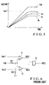
- Fig. 6 shows a conventional power supply voltage detection circuit.
- the power supply voltage detection circuit is constituted by a lower limit comparator 11 for detecting that a power supply voltage VDD becomes equal to or lower than a rated lower limit Vref1, an upper limit comparator 12 for detecting that the power supply voltage VDD becomes equal to or higher than a rated upper limit Vref2, an AND gate 13 for ANDing an output VO11 from the lower limit comparator 11 and an output VO12 from the upper limit comparator 12, and resistors R11 and R12.
- Vref1' Vref1 x R12/(R11 + R12)
- Vref2' Vref2 x R12/(R11 + R12)
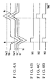
- Figs. 7A to 7D The operation of the power supply voltage detection circuit having the above arrangement will be described with reference to Figs. 7A to 7D.
- the output VO11 from the lower limit comparator 11 is set at "L" level (Low level), as shown in Fig. 7B.
- an output VO13 from the AND gate 13 is also set at "L" level.
- the output VO12 from the upper limit comparator 12 is set at "L" level, as shown in Fig. 7C.
- the output VO13 from the AND gate 13 is also set at "L" level, as shown in Fig. 7D. That the power supply voltage VDD becomes equal to or lower than the rated lower limit Vref1 or equal to or higher than the rated upper limit Vref2 can be detected in this manner.
- Some apparatus such as a microcomputer operates in a wide operating voltage range and can be used with a plurality of power supply voltage ratings (e.g., operable at power supply voltages VDD of 5 V, 3 V,). Obviously, in this case, when the power supply voltage VDD is changed, the rated lower limit Vref1 and the rated upper limit Vref2 also vary accordingly.
- the reference voltage Vref1' for detecting that the power supply voltage VDD becomes equal to or lower than the rated lower limit Vref1 must be applied, together with the reference voltage Vref2' for detecting that the power supply voltage VDD becomes equal to or higher than the rated upper limit Vref2. For this reason, when the rating of the power supply voltage VDD changes, the reference voltages Vref1' and Vref2' must be set again in accordance with the rated lower limit Vref1 and the rated upper limit Vref2.
- this circuit is designed to detect abrupt variations in power supply voltage due to external noise and the like, the circuit also detects moderate variations in power supply voltage (the output VO13 from the AND gate 13 is set at "L" level) during a power-on period (a period PON in Figs. 7A to 7D) or power-off period.
- a power supply voltage detection device comprising reference voltage generating means for generating lower and upper limit reference voltages by resistance-dividing a power supply voltage, integrator means for integrating comparative voltages extracted by resistance-dividing the power supply voltage, lower limit comparison means for comparing the lower limit reference voltage from the reference voltage generating means with an output voltage from the integrator means to detect that the power supply voltage becomes not higher than a lower limit, and upper limit comparison means for comparing the upper reference voltage from the reference voltage generating means with an output voltage from the integrator means to detect that the power supply voltage becomes not lower than an upper limit.
- Fig. 1 shows a power supply voltage detection circuit according to an embodiment of the present invention.
- the power supply voltage detection circuit is constituted by a lower limit comparator 11 for detecting that a power supply voltage VDD becomes equal to or lower than a rated lower limit Vref1, an upper limit comparator 12 for detecting that the power supply voltage VDD becomes equal to or higher than a rated upper limit Vref2, an OR gate 13 for ORing an output VO1 from the lower limit comparator 11 and an output VO2 from the upper limit comparator 12, a reference voltage generating circuit 14 for generating a lower limit reference voltage, an upper limit reference voltage, and a divided voltage by resistance-dividing the power supply voltage VDD, and an integrator circuit 15 for integrating the divided voltage output from the reference voltage generating circuit 14 and outputting the resultant voltage to the lower limit comparator 11 and the upper limit comparator 12.
- the lower and upper limit reference values output from the reference voltage generating circuit 14 are respectively output to the lower limit comparator 11 and the upper limit comparator 12.
- Each of the lower limit comparator 11 and the upper limit comparator 12 is constituted by an operational amplifier having an inverting input terminal and a non-inverting input terminal.
- the reference voltage generating circuit 14 is constituted by resistors R1 to R4 for resistance-dividing the power supply voltage VDD.
- a node A of the resistors R1 and R2 is connected, as a point at which a reference voltage VA is generated, to the inverting input terminal of the lower limit comparator 11.
- a node B of the resistors R3 and R4 is connected, as a point at which a reference voltage VB is generated, to the non-inverting input terminal of the upper limit comparator 12.
- the integrator circuit 15 is constituted by a resistor R5 and a capacitor C1.
- the integrator circuit 15 integrates the voltages at the node of the resistors R2 and R3, and supplies the integral output generated at a point C to the non-inverting input terminal of the lower limit comparator 11 and the inverting input terminal of the upper limit comparator 12.
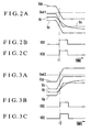
- Figs. 3A to 3C The operation to be performed when the power supply voltage VDD abruptly rises will be described next with reference to Figs. 3A to 3C.
- the reference voltages VA and VB at the points A and B and the voltage VC at the point C also rise accordingly.
- the voltage VC rises more moderately than the reference voltage VB at the point B because the capacitor C1 is charged.
- time t2 the relationship in magnitude between the reference voltage VB at the point B and the voltage VC at the point C is reversed, and the voltage VC becomes lower than the reference voltage VB.
- the output VO2 from the upper limit comparator 12 is set at "H” level, as shown in Fig. 3B, and the output VO3 from the OR gate 13 is also set at "H” level, as shown in Fig. 3C.
- the power supply voltage VDD becomes equal to or higher than the rated upper limit Vref2 can be detected from the output VO3 from the OR gate 13 which has changed to "H" level.
- the operation to be performed when external noise is applied to the power supply voltage VDD is the same as that shown in Figs. 2A to 2C and 3A to 3C. More specifically, the operation to be performed when external noise N1 in Fig. 4A is superimposed is the same as that to be performed when the power supply voltage VDD abruptly changes (drops) below the time constant, at the time of discharging, which is determined by the resistors R3 to R5 and the capacitor C1. In this case, as shown in Figs. 4B and 4D, both the output VO1 from the lower limit comparator 11 and the output VO3 from the OR gate 13 are set at "H" level.
- Fig. 5 shows the operation to be performed when the power supply voltage VDD moderately changes.
- the power supply voltage VDD moderately rises since the relationship in magnitude between the voltage VC and the reference voltage VA or VB is not reversed, both the outputs VO1 and VO2 from the upper limit comparators 11 and 12 are kept at "L" level. Consequently, the output VO3 from the OR gate 13 is also kept at "L” level.
- a similar operation is performed when the power supply voltage VDD moderately drops.
- a time constant is set in the charger/discharger circuit constituted by the resistors R1 to R5 and the capacitor C1 such that the relationship in magnitude between the voltage VC and the reference voltage VA or VB is reversed when the power supply voltage VDD abruptly changes to become equal to or lower than the rated lower limit Vref1 or become equal to or higher than the rated upper limit Vref2 owing to noise or the like.
- a time constant set such that the above relationship in magnitude between the respective voltages does not change when the power supply voltage VDD moderately changes upon power-on or power-off operation. With this setting, only abrupt variations in the power supply voltage VDD can be detected.
- the reference voltages VA and VB automatically vary in accordance with changes in power supply voltage ratings. Unlike in the conventional power supply voltage detection circuit, therefore, when the power supply voltage VDD is changed, the reference voltages need not be set again.
- the degree of change in power supply voltage is determined by the time constant circuit, only abrupt variations in power supply voltage due to external noise and the like can be detected.
- the upper and lower limit reference voltages are generated by resistance-dividing the power supply voltage, the reference voltages need not be set again in accordance with changes in power supply voltage ratings.
Landscapes
- Engineering & Computer Science (AREA)
- Theoretical Computer Science (AREA)
- Physics & Mathematics (AREA)
- General Physics & Mathematics (AREA)
- General Engineering & Computer Science (AREA)
- Measurement Of Current Or Voltage (AREA)
Applications Claiming Priority (3)
| Application Number | Priority Date | Filing Date | Title |
|---|---|---|---|
| JP99083/97 | 1997-04-16 | ||
| JP9908397 | 1997-04-16 | ||
| JP9099083A JPH10288634A (ja) | 1997-04-16 | 1997-04-16 | 電源電圧検出回路 |
Publications (2)
| Publication Number | Publication Date |
|---|---|
| EP0872790A2 true EP0872790A2 (fr) | 1998-10-21 |
| EP0872790A3 EP0872790A3 (fr) | 2003-11-19 |
Family
ID=14238024
Family Applications (1)
| Application Number | Title | Priority Date | Filing Date |
|---|---|---|---|
| EP98106581A Withdrawn EP0872790A3 (fr) | 1997-04-16 | 1998-04-09 | Dispositif de détection d'une tension d'alimentation |
Country Status (4)
| Country | Link |
|---|---|
| US (1) | US6118295A (fr) |
| EP (1) | EP0872790A3 (fr) |
| JP (1) | JPH10288634A (fr) |
| KR (1) | KR100304295B1 (fr) |
Cited By (5)
| Publication number | Priority date | Publication date | Assignee | Title |
|---|---|---|---|---|
| WO2003058417A1 (fr) * | 2001-12-28 | 2003-07-17 | Intel Corporation | Procede et appareil permettant le controle d'une tension d'alimentation a une processeur |
| US6948079B2 (en) | 2001-12-26 | 2005-09-20 | Intel Corporation | Method and apparatus for providing supply voltages for a processor |
| US8058860B2 (en) | 2008-07-02 | 2011-11-15 | Texas Instruments Incorporated | Single pin multi-VID bit interface circuit for dynamic voltage change of a DC/DC converter |
| CN102508011A (zh) * | 2011-09-28 | 2012-06-20 | 青岛海信移动通信技术股份有限公司 | 一种过压失压检测电路及测试装置 |
| CN107741779A (zh) * | 2017-10-23 | 2018-02-27 | 中国船舶重工集团公司第七六研究所 | 一种主处理器模块的atx模式开关 |
Families Citing this family (18)
| Publication number | Priority date | Publication date | Assignee | Title |
|---|---|---|---|---|
| JP2000324804A (ja) * | 1999-04-28 | 2000-11-24 | Ando Electric Co Ltd | 電源供給システムの不良電源検出方法及び装置 |
| JP3578043B2 (ja) | 2000-04-14 | 2004-10-20 | 松下電器産業株式会社 | 電源電圧検出回路 |
| US6348798B1 (en) * | 2000-12-05 | 2002-02-19 | Alpha Smart, Inc. | Analog to digital voltage measuring device |
| US6642706B2 (en) * | 2001-06-13 | 2003-11-04 | Koninklijke Philips Electronics N.V. | Detection of asymmetrical load in an AC circuit |
| US6590412B2 (en) * | 2001-06-26 | 2003-07-08 | Logicvision, Inc. | Circuit and method for detecting transient voltages on a dc power supply rail |
| US7119529B2 (en) * | 2003-06-12 | 2006-10-10 | Koninklijke Philips Electronics N.V. | Circuit arrangement with a resistor voltage divider chain |
| JP3863508B2 (ja) | 2003-07-03 | 2006-12-27 | Necエレクトロニクス株式会社 | 電源電圧検出回路及び半導体集積回路装置 |
| US20050046440A1 (en) * | 2003-08-29 | 2005-03-03 | Alcatel | Fault tolerant vital power supply system |
| US7683591B2 (en) * | 2003-12-26 | 2010-03-23 | Panasonic Corporation | Semiconductor device with voltage variation detector |
| US7358625B2 (en) | 2004-12-14 | 2008-04-15 | Woods Industries, Inc. | Power strip with 12 volt outlet |
| US7719134B2 (en) | 2007-06-12 | 2010-05-18 | Mitsubishi Electric Corporation | In-vehicle mount electronic controller |
| TWI381261B (zh) * | 2008-07-18 | 2013-01-01 | Asia Optical Co Inc | 電源管理裝置以及電源管理方法 |
| CN103033768A (zh) * | 2011-09-30 | 2013-04-10 | 鸿富锦精密工业(深圳)有限公司 | 电源测试系统 |
| CN102798824A (zh) * | 2012-08-13 | 2012-11-28 | 能极电源(深圳)有限公司 | 一种并联电源的串联监测电路及其实现方法 |
| CN104698393A (zh) * | 2013-12-05 | 2015-06-10 | 惠州市德赛西威汽车电子有限公司 | 一种具有自动静音的电源检测器及车载影音系统 |
| JP6903398B2 (ja) * | 2016-01-27 | 2021-07-14 | 三菱電機株式会社 | 駆動装置および液晶表示装置 |
| CN111751017A (zh) * | 2020-07-03 | 2020-10-09 | 格力电器(郑州)有限公司 | 空调感温包检测电路和空调感温包检测装置 |
| CN113359056A (zh) * | 2021-06-01 | 2021-09-07 | 中国航空工业集团公司沈阳飞机设计研究所 | 一种电源有效性自检测电路 |
Family Cites Families (9)
| Publication number | Priority date | Publication date | Assignee | Title |
|---|---|---|---|---|
| DE3132509C2 (de) * | 1981-08-18 | 1984-06-14 | Dynamit Nobel Ag, 5210 Troisdorf | Verfahren und Breitschlitzwerkzeug zur Herstellung einer Farbkeilfolie |
| JPS60250714A (ja) * | 1984-05-28 | 1985-12-11 | Fujitsu Ltd | パワ−・オン・リセツト回路 |
| JPS6395732A (ja) * | 1986-10-09 | 1988-04-26 | Nec Corp | パワ−オンリセツト信号発生回路 |
| JP2687159B2 (ja) * | 1989-02-14 | 1997-12-08 | 松下電器産業株式会社 | 電源投入時のリセットパルス生成回路 |
| JPH02310474A (ja) * | 1989-05-25 | 1990-12-26 | Fanuc Ltd | 電源監視回路 |
| JPH035634A (ja) * | 1989-06-02 | 1991-01-11 | Toshiba Corp | 空気調和機のフィルタ脱着治具 |
| JPH05283994A (ja) * | 1992-04-01 | 1993-10-29 | Nec Ic Microcomput Syst Ltd | リセット回路 |
| US5481194A (en) * | 1994-06-10 | 1996-01-02 | Westinghouse Electric Corp. | Fault detection circuit for sensing leakage currents between power source and chassis |
| US5805068A (en) * | 1995-08-25 | 1998-09-08 | Black & Decker Inc. | Cordless device with battery imbalance indicator |
-
1997
- 1997-04-16 JP JP9099083A patent/JPH10288634A/ja active Pending
-
1998
- 1998-04-09 EP EP98106581A patent/EP0872790A3/fr not_active Withdrawn
- 1998-04-15 KR KR1019980013448A patent/KR100304295B1/ko not_active Expired - Fee Related
- 1998-04-16 US US09/060,827 patent/US6118295A/en not_active Expired - Lifetime
Cited By (6)
| Publication number | Priority date | Publication date | Assignee | Title |
|---|---|---|---|---|
| US6948079B2 (en) | 2001-12-26 | 2005-09-20 | Intel Corporation | Method and apparatus for providing supply voltages for a processor |
| WO2003058417A1 (fr) * | 2001-12-28 | 2003-07-17 | Intel Corporation | Procede et appareil permettant le controle d'une tension d'alimentation a une processeur |
| US8058860B2 (en) | 2008-07-02 | 2011-11-15 | Texas Instruments Incorporated | Single pin multi-VID bit interface circuit for dynamic voltage change of a DC/DC converter |
| CN102508011A (zh) * | 2011-09-28 | 2012-06-20 | 青岛海信移动通信技术股份有限公司 | 一种过压失压检测电路及测试装置 |
| CN107741779A (zh) * | 2017-10-23 | 2018-02-27 | 中国船舶重工集团公司第七六研究所 | 一种主处理器模块的atx模式开关 |
| CN107741779B (zh) * | 2017-10-23 | 2020-10-02 | 中国船舶重工集团公司第七一六研究所 | 一种主处理器模块的atx模式开关 |
Also Published As
| Publication number | Publication date |
|---|---|
| US6118295A (en) | 2000-09-12 |
| JPH10288634A (ja) | 1998-10-27 |
| EP0872790A3 (fr) | 2003-11-19 |
| KR100304295B1 (ko) | 2001-11-02 |
| KR19980081431A (ko) | 1998-11-25 |
Similar Documents
| Publication | Publication Date | Title |
|---|---|---|
| EP0872790A2 (fr) | Dispositif de détection d'une tension d'alimentation | |
| US4849700A (en) | Device for detecting residual capacity of battery | |
| US7911185B2 (en) | Battery voltage detection circuit | |
| JPH10163874A (ja) | スイッチトキャパシタ | |
| JP5550816B2 (ja) | 最適化された計数能力を有する電子センサ | |
| EP1386173B1 (fr) | Circuit de mesure de la capacitance | |
| JP2004032146A (ja) | オフセット電圧キャンセル回路 | |
| JPH0712857A (ja) | モータ電流検出回路 | |
| JP4343489B2 (ja) | 過電流検出遅延回路 | |
| US5625305A (en) | Load detection apparatus | |
| JP2004304334A (ja) | 半導体装置及びリセット信号送出方法 | |
| JP3459552B2 (ja) | 熱感知器 | |
| JP2002186187A (ja) | 二次電池の保護方法およびその回路 | |
| US6184731B1 (en) | Reset signal generation circuit | |
| JP2020173098A (ja) | 周波数検知回路 | |
| JP3148443B2 (ja) | 直流安定化電源装置 | |
| JPH05206811A (ja) | リセット制御回路 | |
| JPH0794942A (ja) | 基準クロック信号生成回路 | |
| JPH0241954Y2 (fr) | ||
| JP2558332Y2 (ja) | 電圧監視回路 | |
| JP2004193803A (ja) | 光受信回路 | |
| JP2568561Y2 (ja) | 電圧検出回路 | |
| JPH0749422Y2 (ja) | 電圧監視回路 | |
| CN118897601A (zh) | 带隙基准电路及其控制方法、集成电路以及电子设备 | |
| JP2932545B2 (ja) | 基準電圧発生回路 |
Legal Events
| Date | Code | Title | Description |
|---|---|---|---|
| PUAI | Public reference made under article 153(3) epc to a published international application that has entered the european phase |
Free format text: ORIGINAL CODE: 0009012 |
|
| AK | Designated contracting states |
Kind code of ref document: A2 Designated state(s): AT BE CH CY DE DK ES FI FR GB GR IE IT LI LU MC NL PT SE |
|
| AX | Request for extension of the european patent |
Free format text: AL;LT;LV;MK;RO;SI |
|
| RAP1 | Party data changed (applicant data changed or rights of an application transferred) |
Owner name: NEC ELECTRONICS CORPORATION |
|
| PUAL | Search report despatched |
Free format text: ORIGINAL CODE: 0009013 |
|
| RIC1 | Information provided on ipc code assigned before grant |
Ipc: 7H 03K 17/22 B Ipc: 7G 06F 1/28 A |
|
| AK | Designated contracting states |
Kind code of ref document: A3 Designated state(s): AT BE CH CY DE DK ES FI FR GB GR IE IT LI LU MC NL PT SE |
|
| AX | Request for extension of the european patent |
Extension state: AL LT LV MK RO SI |
|
| 17P | Request for examination filed |
Effective date: 20031015 |
|
| AKX | Designation fees paid |
Designated state(s): DE FR GB |
|
| 17Q | First examination report despatched |
Effective date: 20050503 |
|
| STAA | Information on the status of an ep patent application or granted ep patent |
Free format text: STATUS: THE APPLICATION HAS BEEN WITHDRAWN |
|
| 18W | Application withdrawn |
Effective date: 20050714 |