EP0872880A2 - Herstellung einer Schicht aus einem Platinmetall für einen Kondensator - Google Patents
Herstellung einer Schicht aus einem Platinmetall für einen Kondensator Download PDFInfo
- Publication number
- EP0872880A2 EP0872880A2 EP97309558A EP97309558A EP0872880A2 EP 0872880 A2 EP0872880 A2 EP 0872880A2 EP 97309558 A EP97309558 A EP 97309558A EP 97309558 A EP97309558 A EP 97309558A EP 0872880 A2 EP0872880 A2 EP 0872880A2
- Authority
- EP
- European Patent Office
- Prior art keywords
- layer
- metal layer
- forming
- contact hole
- barrier layer
- Prior art date
- Legal status (The legal status is an assumption and is not a legal conclusion. Google has not performed a legal analysis and makes no representation as to the accuracy of the status listed.)
- Withdrawn
Links
Images





Classifications
-
- H—ELECTRICITY
- H10—SEMICONDUCTOR DEVICES; ELECTRIC SOLID-STATE DEVICES NOT OTHERWISE PROVIDED FOR
- H10B—ELECTRONIC MEMORY DEVICES
- H10B12/00—Dynamic random access memory [DRAM] devices
-
- H—ELECTRICITY
- H10—SEMICONDUCTOR DEVICES; ELECTRIC SOLID-STATE DEVICES NOT OTHERWISE PROVIDED FOR
- H10D—INORGANIC ELECTRIC SEMICONDUCTOR DEVICES
- H10D1/00—Resistors, capacitors or inductors
- H10D1/60—Capacitors
- H10D1/68—Capacitors having no potential barriers
- H10D1/692—Electrodes
-
- H—ELECTRICITY
- H10—SEMICONDUCTOR DEVICES; ELECTRIC SOLID-STATE DEVICES NOT OTHERWISE PROVIDED FOR
- H10W—GENERIC PACKAGES, INTERCONNECTIONS, CONNECTORS OR OTHER CONSTRUCTIONAL DETAILS OF DEVICES COVERED BY CLASS H10
- H10W20/00—Interconnections in chips, wafers or substrates
- H10W20/01—Manufacture or treatment
- H10W20/031—Manufacture or treatment of conductive parts of the interconnections
- H10W20/056—Manufacture or treatment of conductive parts of the interconnections by filling conductive material into holes, grooves or trenches
- H10W20/059—Manufacture or treatment of conductive parts of the interconnections by filling conductive material into holes, grooves or trenches by reflowing or applying pressure
Definitions
- the present invention relates to a method for fabricating a semiconductor device, and more particularly, to a method for forming a metal layer from a platinum group metal and a method for fabricating a capacitor utilizing the same.
- a barrier layer is necessary for preventing a reaction of the platinum group metal with polysilicon used for a conductive plug or with a substrate silicon, and for preventing diffusion of oxygen used as a source during deposition of a dielectric layer.
- Figures 1A and 1B are sectional views illustrating a conventional method for forming a capacitor storage electrode using platinum.
- an insulating layer 12 formed on a semiconductor substrate 10 is partially etched to form a storage contact hole 14, and then polysilicon is deposited and etched back to form a conductive plug 16 for filling the storage contact hole 14.
- a titanium nitride layer 18 as a barrier layer is formed on the resultant structure where the conductive plug 16 is formed, and platinum is deposited on the titanium nitride layer 18 to form a platinum layer 20.
- an oxide layer to be used as an etching mask is formed on the resultant structure where the platinum layer 20 is formed, and patterned to form a mask pattern 22.
- the platinum layer 20 and the titanium nitride layer 18 are sequentially etched to form a platinum layer pattern 24 and a barrier layer pattern 26.
- a dielectric layer 28 formed of BST or PZT is deposited on a substrate where the conductive plug 16 and a storage electrode 27 including the barrier layer pattern 26 and the platinum layer pattern 24 is formed, through a sputtering method or a metal organic chemical vapor deposition(MOCVD) method. Then, a plate electrode 30 is formed on the resultant structure.
- the dielectric layer 28 When the dielectric layer 28 is formed in a state where the side surfaces of the barrier layer pattern 26 are exposed, after forming the platinum layer pattern 24, oxygen is easily diffused from the side surfaces of the barrier layer pattern 26.
- the oxygen atmosphere and the high temperature in which the high dielectric layer 28 such as BST or PZT is formed accelerate the oxygen diffusion.
- the barrier layer pattern 26 Due to the oxygen diffusion, the barrier layer pattern 26 is partially oxidized, and a titanium oxide layer TiO 2 (not shown) which has an insulating characteristic is formed on an interface between the conductive plug 16 and the barrier layer pattern 26, or between the barrier layer pattern 26 and the platinum layer pattern 24.
- the titanium oxide layer causes contact failure, and deteriorates the function of the barrier layer 26 by allowing diffusion of oxygen or metal atoms therethrough, to generate leakage current between the storage electrode 27 and the semiconductor substrate 10.
- the storage electrode in particular the platinum layer pattern 24, is required to be thickly formed, it impedes patterning and generates a high step difference around the capacitor.
- the platinum layer pattern 24 of the storage electrode is thin, oxygen passes through the platinum layer pattern 24 to combine with the barrier layer pattern 26. Accordingly, the platinum layer pattern 24 is 2000 ⁇ thick or more.
- the platinum is very hard and refractory, it cannot easily react with a different chemical material and cannot be easily etched through dry etching such as reactive ion etching. Accordingly, when the platinum layer pattern is 2000 ⁇ thick or more, the patterning becomes very difficult, while the platinum layer pattern has great step difference around the capacitor.
- the etching mask requires an etch rate lower than that of the material layer to be etched.
- the platinum group metal has difficulties in etching. Therefore, it is very difficult to obtain an etching mask having an etch rate lower than that of the platinum group metal.
- a method for forming a platinum group metal layer comprising the steps of:
- the material layer is formed of an undoped silicate glass.
- the platinum group metal is one selected from the group consisting of Pt, Ru, Ir, Rh, Os, RuO 2 , and IrO 2 .
- the platinum group metal is formed having a thickness in the region of 1000 to 2000 ⁇ .
- the reflowing is performed in an N 2 atmosphere, in the region of 650 to 900°C, and for in the region of 5 minutes to 1 hour.
- a method for manufacturing a capacitor comprising the steps of:
- the method contains the step of:
- the method contains the step of:
- the method contains the step of:
- said step of forming the conductive plug comprises the sub-steps of:
- said step of forming the conductive plug comprises the sub-steps of:
- the barrier layer formed on the interlayer dielectric is removed to form the barrier layer only in the storage contact hole, and wherein only the metal layer is patterned during the step of forming the storage electrode pattern.
- the barrier layer is formed of one selected from the group consisting of TiN, CoSi, TaSiN, TiSiN, TaSi, TiSi, Ta and TaN.
- a method for manufacturing a capacitor comprising the steps of:
- the metal layer pattern is formed by chemical-mechanical polishing the reflowed metal layer until the etch stopper is exposed.
- the method further comprises the step of removing the etch stopper, to thereby form the dielectric layer on the upper and the side surfaces of the metal layer pattern, after said step i).
- the method further comprises the step of:
- the metal layer is formed by blanket etching back the reflowed metal layer and the etch stopper until the etching barrier layer is exposed.
- the etch stopper is formed of an oxide and the etching barrier layer is formed of a nitride.
- a method for manufacturing a capacitor comprising the steps of:
- the metal layer pattern is formed by chemical mechanical polishing the reflowed metal layer until the etch stopper is exposed.
- the metal layer pattern is formed by etching back the reflowed metal layer and the etch stopper until the barrier layer is exposed.
- the method comprises the step of:
- a method for manufacturing a capacitor comprising the steps of:
- the method further comprises the step of:
- the method further comprises the step of:
- the metal layer pattern is formed by chemical-mechanical polishing the reflowed metal layer until the etch stopper is exposed.
- the metal layer pattern is formed by blanket etching back the reflowed metal layer and the etch stopper until the etching barrier layer is exposed.
- the method further comprises the step of:
- the interlayer dielectric is formed of an oxide undoped with impurities.
- the metal layer is formed of one selected from the group consisting of Pt, Ru, Ir, Rh, Os, RuO 2 and IrO 2 .
- the metal layer is formed of platinum Pt.
- the dielectric layer is formed of one selected from the group consisting of Ba(Sr,Ti)O 3 , Pb(Zr,Ti)O 3 , Ta 2 O 5 , SiO 2 , SiN 3 , SrTiO 3 , PZT, SrBi 2 Ta 2 O 9 , (Pb, La)(Zr, Ti)O 3 , and Bi 4 Ti 3 O 12 .
- the metal layer is formed having a thickness in the region of 1000 to 2000 ⁇ .
- the relowing is performed by heating at more than 650°C.
- the reflowing is performed in an N 2 atmosphere, in the region of 650 to 900°C, and for in the region of 5 minutes to 1 hour.
- a platinum group metal layer is formed on a semiconductor substrate preferably having a material layer of undoped silicate glass where an opening such as a storage contact hole is formed having a thickness of the order of 1000 ⁇ 2000 ⁇ , and then the platinum group metal layer is reflowed at 650°C or more to fill the opening.
- the platinum group metal layer is reflowed to form the storage electrode of the capacitor. That is, a barrier layer and the platinum group metal layer are formed in the storage contact hole formed on a semiconductor substrate, and then the platinum group metal layer is reflowed to fill the storage contact hole. Subsequently, the platinum group metal layer and the barrier layer are patterned, to form a storage electrode including the platinum group metal layer pattern and the barrier layer pattern. Also, before forming the barrier layer, a conductive plug for filling a portion of the storage contact hole may be formed to enhance an aspect ratio of the storage contact hole.
- the platinum group metal layer becomes thicker than conventional one as much as a filling depth of the storage contact hole.
- a diffusion distance that the oxygen infiltrated through the surface of the platinum group metal layer and the side surfaces of the barrier layer contacts with the portion serving as the barrier layer becomes long. Therefore, oxidation of the barrier layer can be constrained, and the contact failure of the storage electrode can be prevented.
- the patterning is more easily performed than that of the conventional art, and a step difference from the portion around the capacitor is reduced.
- a conductive plug and a barrier layer for filling the storage contact hole passing through an interlayer dielectric are formed.
- An etch stopper having an opening portion where the storage electrode is to be formed is formed on the interlayer dielectric, and the platinum group metal layer is formed and reflowed, to fill the opening portion and the storage contact hole. Then, the platinum group metal layer on the interlayer dielectric is removed by chemical-mechanical polishing (CMP) or etchback, and the etch stopper is removed, to form a storage electrode including the platinum group metal layer pattern and the barrier layer pattern.
- CMP chemical-mechanical polishing
- the platinum group metal layer pattern can be formed through CMP or etchback without using an etching mask, a mask having a high etching selectivity with respect to the metal layer of the platinum group is not required.
- the barrier layer is formed in the storage contact hole formed on the interlayer dielectric and passing through the interlayer dielectric.
- a conductive plug for filling a portion of the storage contact hole can be formed to enhance the aspect ratio of the storage contact hole.
- an etch stopper having an opening portion where the storage electrode is to be formed is formed, and then the platinum group metal layer is formed and reflowed, to fill the opening portion and the storage contact hole.
- the platinum group metal layer on the interlayer dielectric is removed through CMP or etchback, and the etch stopper is removed to form a platinum group metal layer pattern, and the barrier layer is patterned using the platinum group metal layer pattern as a mask to form a storage electrode.
- the platinum group metal layer becomes thicker as much as a filling depth of the storage contact hole, to thereby prevent the contact failure of the storage electrode, and the platinum group metal layer pattern can be formed without an etching mask.
- FIG. 2A is a sectional view showing the step of forming a platinum layer 44.
- an insulating layer 42 is formed on a semiconductor substrate 40, and the insulating layer 42 is partially etched to form an opening 43, and then a metal of the platinum group, for example, platinum, is deposited on the entire surface of the resultant structure where the opening 43 is formed, through a sputtering method to form a platinum layer 44.
- the platinum layer 44 is formed in a predetermined thickness, for example, 1000 ⁇ 2000 ⁇ , and it is possible to use Ru, Ir, Rh, Os, RuO 2 or IrO 2 instead of the platinum.
- Figure 2B is a sectional view showing the step of forming a reflowed platinum layer 46.
- the resultant structure where the platinum layer 44 is formed is introduced into a furnace, for example, a typical quartz tube, and the platinum layer 44 is reflowed, to fill the opening 43 and obtain a platinum layer 46 having a planarized surface.
- the platinum layer 44 is reflowed in nitrogen (N2) ambient for around 5 minutes to 1 hour at around 650°C to 900 °C.
- Figure 3A is a SEM photograph showing a state in which an undoped silicate glass is deposited on a silicon substrate in a thickness of approximately 4000 ⁇ to form an insulating layer, which is patterned to have an insulating layer surface where openings having a predetermined depth are formed, and then a platinum layer is deposited on the entire surface of the resultant structure in a thickness of approximately 1000 ⁇ using a sputtering method.
- Figure 3B is a SEM photograph showing a result in which the resultant structure where the platinum layer is formed is introduced in the quartz tube, and then thermally treated for approximately 30 minutes in nitrogen ambient at 750°C.
- the platinum layer is reflowed by thermal treating, to fill the openings formed on the insulating surface and form a planarized platinum layer 46.
- the method for forming the platinum group metal layer using the reflow of the platinum group metal can be variously applied.
- a storage electrode of a capacitor is formed by the above method, it is possible to prevent contact failure of the storage electrode due to diffusion of oxygen infiltrated through the side surfaces of the barrier layer and easily form the storage electrode.
- Figure 4A is a sectional view showing a step of forming a storage contact hole 54.
- an insulating material for example, an undoped silicate glass (USG)
- USG undoped silicate glass
- Figure 4B is a sectional view showing a step of forming a barrier layer 60.
- a barrier metal for example, titanium nitride
- a barrier metal for example, titanium nitride
- the barrier layer 60 is formed on the entire inside of the storage contact hole 54 as well as on the interlayer dielectric 55.
- the barrier layer 60 is selected from the group consisting of a refractory metal including titanium nitride, for example, TiN, CiSi, TaSiN, TiSiN, TaSi, TiSi, Ta, TaN, and an oxide of the platinum group metal.
- a metal silicide layer for example, a titanium silicide layer
- a metal silicide layer is formed on a substrate surface such that ohmic contact with a silicon substrate is formed to reduce contact resistance of the storage electrode.
- the titanium silicide layer can be formed by depositing titanium and then annealing it.
- a material capable of forming a silicide with the silicon substrate i.e., tungsten nitride (WN) or tungsten (W), can be also used.
- FIG. 4C is a sectional view showing a step of forming a platinum layer 65.
- a platinum group metal to be used as a storage electrode for example, platinum, is deposited on the barrier layer 60 through a sputtering method, to form a platinum layer 65.
- the platinum layer 65 is formed in a thickness of approximately 1000 to 2000 ⁇ .
- Ru, Ir, Rh, Os, and an oxide thereof can be used.
- an oxygen diffusion barrier layer (not shown) for preventing diffusion of oxygen passing through the platinum layer can be further formed between the barrier layer 60 and the platinum layer 65, where Ir, Ru, RuO2, IrO2 or a combined layer thereof can be used for the oxygen diffusion barrier layer.
- Figure 4D is a sectional view showing a step of reflowing the platinum layer 65 of Figure 4C.
- the resultant structure where the platinum layer 65 is formed is introduced in a furnace, for example, a quartz tube, and then the platinum layer 65 is reflowed by heating, to fill the storage contact hole 54 and obtain a platinum layer 70 having a planarized surface.
- the reflowing preferably, is performed in N2 ambient at 650°C to 900°C, and for 5 minutes to 1 hour.
- Figure 4E is a sectional view showing the step of forming a storage electrode 82.
- an insulating material for example, an oxide
- an insulating material for example, an oxide
- the planarized platinum layer 70 of Figure 4D and the barrier layer 60 of Figure 4D are sequentially etched using the mask pattern, to form the storage electrode 82 comprised of the platinum layer pattern 75 and the barrier layer pattern 80.
- a distance between the barrier layer pattern 80 formed on the bottom surface of the storage contact hole 54 and the surface of the platinum layer pattern 75 can be sufficiently maintained, which is equal to a distance obtained by adding a depth of a storage contact hole, a thickness of a platinum layer pattern and a thickness of a barrier layer pattern. That is, oxygen used during the process of forming a dielectric layer does not pass through the platinum layer pattern 75 and is prevented from combining with the barrier layer pattern 80 formed on the bottom surface of the storage contact hole.
- oxygen can be prevented by the platinum layer from combining with the barrier layer, even though the platinum layer pattern 75 is not very thick or distant from the surface of the interlayer dielectric 55. Also, even though oxygen may infiltrate into the side of the barrier layer 80, the diffusion distance to the bottom surface of the storage contact 54 is relatively long, to thereby constrain formation of a titanium oxide layer due to the oxygen diffusion.
- Figure 4F is a sectional view showing a step of forming a dielectric layer 85 and a plate electrode 90.
- a dielectric material for example, BST
- BST a dielectric material
- the dielectric material instead of the BST can be formed of one selected from the group consisting of Ta 2 O 5 , SiO 2 , SiN 3 , SrTiO 3 , PZT, SrBi 2 Ta 2 O 9 , (Pb,La)(Zr,Ti)O 3 , Bi 4 Ti 3 O 12 , and a combination thereof.
- a platinum layer is reflowed to fill a storage contact hole without forming a conductive plug. Accordingly, a diffusion distance of oxygen through a platinum layer pattern 75 and through the side of a barrier layer pattern 80 becomes long, such that the oxygen rarely reaches the barrier layer formed on the bottom surface of the storage contact hole. Therefore, oxidation of the barrier layer can be constrained, to thereby prevent contact failure of the storage electrode and generation of leakage current arising from the diffusion of oxygen or metal atoms. As a result, deterioration of electrical characteristics of a semiconductor device can be prevented. Also, since the storage electrode is not thick, patterning can be easily performed and a step difference from a portion around the capacitor can be reduced.
- Figures 5A and 5B are sectional views for illustrating a second embodiment of the method for manufacturing a capacitor.
- the second embodiment is performed in the same manner as that of the first embodiment except for the step of forming a conductive plug 57 for filling a portion of the storage contact hole 54.
- Figure 5A is a sectional view showing a step of forming the conductive plug 57 and the barrier layer 60.
- the step of patterning an interlayer dielectric 55 to form the storage contact hole 54 is performed in the same manner as that of the first embodiment.
- a conductive material for example, polysilicon, is deposited on the entire surface of the resultant structure where the storage contact hole is formed, to fill the storage contact hole 54 and a conductive layer having a predetermined thickness is formed on the interlayer dielectric 55.
- the conductive layer is partially eliminated to form a conductive plug 57 for filling the storage contact hole to a portion of the total depth. Then, the barrier layer 60 is formed on the entire surface of the substrate, including where the conductive plug 57 is formed, in the same manner as the first embodiment.
- the conductive plug 57 can be formed by eliminating a conductive layer on the interlayer dielectric through an etchback process, and then overetching the conductive layer filling the storage contact hole 54.
- the conductive layer on the interlayer dielectric 55 is removed through a CMP process instead of the etchback process, and an etching selectivity of the interlayer dielectric with respect to the conductive layer is controlled by the removal rate of the CMP process to form the conductive plug 57 filling a portion of the storage contact hole 54.
- Figure 5B is a sectional view showing a step of forming a capacitor formed of a storage electrode 82, a dielectric layer 85, and a plate electrode 90.
- the storage electrode 82 formed of the platinum layer pattern 75 and the barrier layer pattern 80 in the same manner as that shown in Figures 4C through 4E, on the resultant structure having the conductive plug 57 are formed.
- the dielectric layer 85 and the plate electrode 90 are formed on the substrate having the storage electrode 82 to thereby complete a capacitor.
- a filling depth of the storage contact hole by the conductive plug 57 i.e., a thickness of the conductive plug 57, is determined by an aspect ratio of the storage contact hole.
- the aspect ratio of the storage contact hole is high, it is preferable that the conductive plug 57 is thick.
- the aspect ratio of the storage contact hole is high.
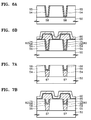
- Figures 6A and 6B are sectional views for illustrating a third embodiment of the method for manufacturing a capacitor.
- the third embodiment is performed in the same manner as that in the first embodiment except for a step of removing the barrier layer formed on a region outside the storage contact hole 54 after forming the barrier layer 60 of Figure 4B.
- Figure 6A is a sectional view showing a step of forming a barrier layer 58.
- the steps for forming the storage contact hole 54 and the barrier layer 60 are performed in the same manner as that of the first embodiment.
- the barrier layer formed on the interlayer dielectric 55 is removed through the CMP process or the etchback process, to form the barrier layer pattern 58 in the storage contact hole 54.
- Figure 6B is a sectional view showing a step of forming a storage electrode 82, a dielectric layer 85 and a plate electrode 90.
- the storage electrode 82 including a platinum layer pattern 75 and a barrier layer pattern 58 is formed on the resultant structure where the barrier layer pattern 58 is formed, through forming a platinum layer, reflowing and patterning it in the same manner as in Figures 4C through 4E.
- the dielectric layer 85 and the plate electrode 90 are formed on a substrate where the storage electrode 82 is formed, to complete a capacitor.
- the barrier layer pattern 58 is formed in the storage contact hole, so that the side of the barrier layer pattern during forming the dielectric layer 85 is not exposed. Therefore, oxidation of the barrier layer can be effectively constrained.
- Figures 7A and 7B are sectional views for illustrating a fourth embodiment of the method for manufacturing a capacitor.
- the fourth embodiment is performed as the same manner as the third embodiment except for a process of forming a conductive plug 57 for filling a portion of the storage contact hole 54.
- the conductive plug 57 for filling a portion of the storage contact hole is formed like the second embodiment (see Figure 5A), and then a barrier layer is formed on the entire surface of the substrate where the conductive plug 57 is formed.
- the barrier layer formed on the interlayer dielectric 55 is removed through a CMP process or an etchback process as shown in the third embodiment (see Figure 6A) to form a barrier layer pattern 58 in the storage contact hole 54.
- Figure 7B is a sectional view showing a step of forming a storage electrode 82, a dielectric layer 85 and a plate electrode 90.
- a capacitor including the storage electrode 82, the dielectric layer 85 and the plate electrode 90 is completed in the same manner as the third embodiment (see Figure 6B).
- the storage contact hole 54 is partially filled with the conductive plug 57, as shown in the second embodiment, it is advantageous that the aspect ratio of the storage contact hole is high. Further, since the barrier layer pattern 58 is formed only in the storage contact hole, as shown in the third embodiment, the side surfaces of the barrier layer pattern 58 during forming the dielectric layer 85 are not exposed.
- platinum is reflowed to form a platinum layer pattern for filling all or a portion of the storage contact hole, to thereby maintain a sufficient distance between the surface of platinum layer pattern and the barrier layer pattern, or between the surface of platinum layer pattern and the silicon substrate (or the conductive plug). Accordingly, even though the platinum layer is not thickly formed, oxygen is prevented from passing through the platinum layer and therefore cannot combine with the barrier layer. Also, even though oxygen is infiltrated into the side of the platinum layer, since the diffusion distance becomes long, formation of an oxide layer, i.e., a titanium oxide layer, due to oxygen diffusion, at an interface between the barrier layer pattern and the platinum layer pattern can be constrained.
- an oxide layer i.e., a titanium oxide layer
- the etching mask for forming a platinum layer pattern.
- the platinum is hard and refractory, it is difficult to obtain a mask having an etch rate lower than that of the platinum.
- the platinum layer pattern can be formed using the platinum reflow without a mask, which will be in detail described with reference to the fifth and sixth embodiments.
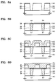
- Figures 8A through 8F are sectional views for illustrating a fifth embodiment of a method for manufacturing a capacitor .
- Figure 8A is a sectional view showing a step of forming a storage contact hole 54.
- an insulating material such as undoped silicate glass (USG) and a nitride, is sequentially deposited on a semiconductor substrate 50, to form an interlayer dielectric 55 and an etching barrier layer 56, and then patterned to form a storage contact hole 54 exposing a predetermined portion of the substrate 50.
- USG undoped silicate glass
- a nitride is sequentially deposited on a semiconductor substrate 50, to form an interlayer dielectric 55 and an etching barrier layer 56, and then patterned to form a storage contact hole 54 exposing a predetermined portion of the substrate 50.
- the etching barrier layer 56 is formed for preventing the interlayer dielectric 55 from being etched during patterning an etch stopper 63 of Figure 8C to be formed. Also, when the etch stopper is formed of a material having an etching selectivity higher than that of the interlayer dielectric 55, the etching barrier layer 56 may not be formed.
- Figure 8B is a sectional view showing a step of forming a conductive plug 57 and a barrier layer pattern 59.
- a conductive material such as polysilicon doped with impurities, is deposited on the entire surface of the substrate where the storage contact hole 54 is formed, to form a conductive layer for burying the storage contact hole 54, and then planarized through an etchback process or a CMP process, and further the conductive layer formed in the storage contact hole is partially overetched to form the conductive plug 57.
- an overetched depth is equal to a thickness of the barrier layer.
- the barrier metal such as a titanium nitride
- the barrier metal is deposited on the entire surface of the substrate where the conductive plug 57 is formed, through a CVD method, and then etched until the etching barrier 56 is exposed, to form a barrier layer pattern 59 on the conductive plug 57.
- the refractory metal as described in the first embodiment instead of titanium nitride can be used as the barrier metal, and the metal silicide layer for forming an ohmic contact layer can be formed between the barrier layer pattern 59 and the conductive plug 57.
- barrier layer pattern 59 is formed such that the upper end of the storage contact hole opened by overetching the conductive plug 57 is filled, the side thereof is not exposed.
- FIG 8C is a sectional view showing a step of forming an etch stopper 63 and a platinum layer 65.
- a material having a high wet etching selectivity to platinum i.e., an oxide
- platinum is deposited on the etching barrier layer 56 and the barrier layer pattern 59, and then patterned, to form an etch stopper 63 having an opening portion where the storage electrode is to be formed.
- a platinum group metal to be used as a storage electrode i.e., platinum
- the platinum layer 65 is formed in a thickness of 1000 ⁇ 2000 ⁇ like the first embodiment (see Figure 4C), and it can be formed through a sputtering method.
- FIG. 8D is a sectional view showing a step of reflowing the platinum layer 65.
- the platinum layer 65 is reflowed in the same manner as the first embodiment, to fill a portion opened by the etch stopper 63 and obtain a platinum layer 70 having a planarized surface.
- Figure 8E is a sectional view showing a step of forming a storage electrode 82.
- the CMP process for the planarized platinum layer 70 is performed until the etch stopper 63 is exposed, to form a platinum layer pattern 75.
- the storage electrode 82 including the platinum layer pattern 75, and a barrier layer pattern 59 is formed.
- the platinum layer pattern 75 formed through the CMP process does not require an etching mask, which is necessary for the conventional art.
- Figure 8F is a sectional view showing a step of forming a dielectric layer 85 and a plate electrode 90.
- a dielectric material such as BST or PZT, is deposited on the substrate where the storage electrode 82 is formed, through a sputtering method, to form the dielectric layer 85.
- the plate electrode 90 is formed on the dielectric layer 85 to complete a capacitor.
- the etch stopper 63 can be removed using an etchant, i.e., buffered oxide etchant (BOE) before forming the dielectric layer 85.
- a dielectric material i.e., BST or PZT, can be deposited on the entire surface of the resultant structure through a CVD method, to form the dielectric layer 85. Therefore, capacitance can be effectively increased due to increase in an effective area of the storage electrode.
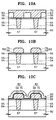
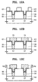
- FIGS 10A through 10C are sectional views for illustrating a sixth embodiment of a method for manufacturing a capacitor.
- the sixth embodiment is performed in the same manner as the fifth embodiment, except for etchback instead of the CMP with respect to the planarized platinum layer 70, to form a platinum layer pattern.
- FIG 10A shows a step of forming a planarized platinum layer 70.
- the planarized platinum layer 70 is obtained in the same manner as those shown in Figures 8A through 8D of the fifth embodiment.
- Figure 10B is a sectional view showing a step of forming a platinum layer pattern 76.
- the platinum layer pattern 75 of Figure 8E is formed through the CMP method, entire surfaces of the planarized platinum layer pattern 70 and an etch stopper 63 are blanket- etched back.
- the etchback is performed until the etching barrier layer 56 is exposed, to thereby form the platinum layer pattern 76 having a cut upper edge as shown in Figure 10A.
- FIG. 10C is a sectional view showing a step of forming a dielectric layer 85 and a plate electrode 90.
- the dielectric layer 85 and the plate electrode 90 are formed on the storage electrode 82 including the barrier layer pattern 59 and the platinum layer pattern 76, to complete a capacitor.
- the etch stopper 63 having an opening portion is formed and the platinum is deposited and reflowed, to fill the opening portion of the etch stopper, and further the platinum layer pattern is formed by performing the CMP or the etchback process. Accordingly, the etching mask for forming the platinum layer pattern 75 is not necessary, and further the platinum layer pattern 75 can be easily formed.
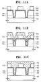
- Figures 11A through 11E are sectional views for illustrating a seventh embodiment of a method for manufacturing a capacitor.
- the seventh embodiment which can be obtained by combining the first embodiment (see Figures 4A through 4F) with the fifth embodiment (see Figures 8A through 8F)
- the barrier layer is formed in the storage contact hole (refer to the first embodiment)
- the platinum layer pattern is formed without an etching mask (refer to the fifth embodiment).
- Figure 11A is a sectional view showing a step of forming a barrier layer 60 and an etch stopper 63.
- the interlayer dielectric 55, the storage contact hole 54 and the barrier layer 60 are formed on the semiconductor substrate 50, and then as shown in Figure 8C of the fifth embodiment, the etch stopper 63 in which a portion where the storage electrode is to be formed is open, is formed.
- FIG 11B is a sectional view showing a step of forming a platinum layer 65.
- the platinum layer 65 is formed on the entire surface of the substrate where the etch stopper 63 is formed.
- FIG 11C is a sectional view showing a step of forming a planarized platinum layer 70.
- the platinum layer 65 is reflowed like the first embodiment, to bury a portion opened by the storage contact hole 54 and the etch stopper 63.
- Figure 11D is a sectional view showing a step of forming a platinum layer pattern 75.
- a planarization process for example, a CMP, is performed until the etch stopper 63 is exposed, to form the platinum layer pattern 75.
- Figure 11E is a sectional view showing a step of forming a storage electrode 82.
- the etch stopper 63 of Figure 11D is removed, and then the barrier layer 60 of Figure 11D is etched using the platinum layer pattern 75 as an etching mask to form a barrier layer pattern 80. Therefore, the storage electrode 82 including the platinum layer pattern 75 and the barrier layer pattern 80 is formed.
- a dielectric layer and a plate electrode are formed in the same manner as that of the first embodiment.
- the storage electrode in the seventh embodiment has the same structure as that of the first embodiment (see Figure 4E). Accordingly, like in the first embodiment, during forming the dielectric layer, a distance of oxygen diffused from the surface of the platinum layer pattern 75 and from the side of the barrier layer pattern 80 becomes long, and thus contact failure of the storage electrode does not occur. Also, like in the fifth embodiment, the platinum layer pattern 75 can be formed without an etching mask.
- FIGS 12A through 12C are sectional views for illustrating an eighth embodiment of a method for manufacturing a capacitor.
- the eighth embodiment which is obtained by combining the second embodiment (see Figures 5A and 5B) with the fifth embodiment (see Figures 8A through 8F), is performed in the same manner as that of the seventh embodiment, except a process of forming a conductive plug 57 for filling a portion of the storage contact hole 54.
- the conductive plug 57 for filling a portion of the storage contact hole 54 and the barrier layer 60 are formed in the same manner as that of the second embodiment, and then an etch stopper 63 is formed with having an opening portion where the storage electrode is to be formed.
- a platinum layer pattern 75 is formed as shown in Figures 12B and 12C and the etch stopper 63 is removed, and then a storage electrode 82 including the platinum layer pattern 75 and the barrier layer pattern 80 is formed.
- the storage electrode 82 of the eighth embodiment has the same structure of the storage electrode (see Figure 5B) of the second embodiment. Therefore, it is advantageous that the aspect ratio of the storage contact hole is high, like the second embodiment, and the platinum layer pattern can be formed without an etching mask to simplify a manufacturing process, compared with the second embodiment.
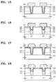
- FIGS 13A through 13C are sectional views for illustrating a ninth embodiment of a method for manufacturing a capacitor.
- the ninth embodiment which is obtained by combining the first embodiment (see Figures 4A through 4F) with the sixth embodiment (see Figures 10A through 10C), is performed in the same manner as that of the seventh embodiment except for blanket-etching back the planarized platinum layer (70 of Figures 11C and 13A) during forming a platinum layer pattern.
- the steps for forming the planarized platinum layer 70 are performed in the same manner as shown in the seventh embodiment, and then the planarized platinum layer 70 and the etch stopper 63 are blanket-etched back as in the sixth embodiment (see Figure 10B), to form a platinum layer pattern 76 having cut upper edges ( Figure 13B).
- the barrier layer 60 is etched using the platinum layer pattern 76 as a mask, to form a storage electrode 82 including the platinum layer pattern 76 and the barrier layer pattern 80.
- Figure 14 is a sectional view for illustrating a tenth embodiment of the method for manufacturing a capacitor, which is obtained by combining the second embodiment (see Figures 5A and 5B) with the sixth embodiment (see Figures 10A through 10C), and is the same as the ninth embodiment except for forming a conductive plug 57 filling a portion of the storage contact hole 54.
- Figure 15 is a sectional view for illustrating an eleventh embodiment of the method for manufacturing a capacitor which is obtained by combining the third embodiment (see Figures 6A and 6B) and the fifth embodiment (see Figures 8A through 8F), and is the same as the seventh embodiment except for forming the barrier layer pattern 58 only in the storage contact hole 54.
- the barrier layer pattern 58 in the storage contact hole is formed, and an etch stopper 63 of Figure 11D and a platinum layer pattern 75 are formed on the resultant structure where the barrier layer pattern 58 is formed and the etch stopper is removed in the same manner as that of the seventh embodiment (see Figures 11A through 11D).
- an etching barrier layer 56 for preventing the interlayer dielectric 55 from being etched is formed, however, it need not be formed in the case that the etch stopper is formed of a material having a high etching selectivity with respect to the interlayer dielectric 55.
- Figure 16 is a sectional view for illustrating a twelfth embodiment of the method for manufacturing a capacitor, which is obtained by combining the fourth embodiment (see Figures 7A and 7B) with the fifth embodiment (see Figures 8a through 8F), and is the same as the eleventh embodiment except for forming the conductive plug 57 filling a portion of the storage contact hole 54, as shown in Figure 16.
- Figure 17 is a sectional view for illustrating a thirteenth embodiment of a manufacturing method, which is obtained by combining the third embodiment (see Figures 6A and 6B) with the sixth embodiment (see FIGS 10A. through 10C), and is the same as the eleventh embodiment except for forming the platinum layer pattern 76 having slantingly cut edges through the etchback.
- Figure 18 is a sectional view for illustrating a fourteenth embodiment which is obtained by combining the fourth embodiment (see Figures 7A and 7B) with the sixth embodiment(see Figures 10A through 10C), and is the same as the thirteenth embodiment except for forming a conductive plug 57 filling a portion of the storage contact hole 54.
- the method described herein for forming the platinum group metal layer using reflow has many advantages in forming a storage electrode of a capacitor, as follows.
- deterioration can be inhibited of the electrical characteristics of a semiconductor device due to oxygen diffusion through the upper surface of the platinum layer pattern and the side of the exposed barrier layer during formation of a dielectric layer.
- the platinum layer pattern and the barrier layer pattern contact with a substrate or a conductive plug in the storage contact hole. That is, a distance between the surface of the platinum layer pattern and the barrier layer pattern is maintained such that oxygen infiltrating through the surface of the platinum layer pattern and the side of the barrier layer pattern cannot reach the barrier layer which contacts with the substrate or the conductive plug. Accordingly, since the distance of oxygen diffusion is long, an oxide layer, for example, a titanium oxide layer is rarely formed at an interface between the barrier layer pattern and the platinum layer pattern.
- the metal pattern of the platinum group can be more easily formed than in the conventional art.
Landscapes
- Semiconductor Memories (AREA)
- Semiconductor Integrated Circuits (AREA)
- Electrodes Of Semiconductors (AREA)
- Physical Vapour Deposition (AREA)
- Internal Circuitry In Semiconductor Integrated Circuit Devices (AREA)
Applications Claiming Priority (2)
| Application Number | Priority Date | Filing Date | Title |
|---|---|---|---|
| KR9714195 | 1997-04-17 | ||
| KR1019970014195A KR100230418B1 (ko) | 1997-04-17 | 1997-04-17 | 백금족 금속층 형성방법 및 이를 이용한 커패시터 제조방법 |
Publications (2)
| Publication Number | Publication Date |
|---|---|
| EP0872880A2 true EP0872880A2 (de) | 1998-10-21 |
| EP0872880A3 EP0872880A3 (de) | 1999-10-06 |
Family
ID=19503053
Family Applications (1)
| Application Number | Title | Priority Date | Filing Date |
|---|---|---|---|
| EP97309558A Withdrawn EP0872880A3 (de) | 1997-04-17 | 1997-11-27 | Herstellung einer Schicht aus einem Platinmetall für einen Kondensator |
Country Status (5)
| Country | Link |
|---|---|
| US (1) | US6001660A (de) |
| EP (1) | EP0872880A3 (de) |
| JP (1) | JP4510943B2 (de) |
| KR (1) | KR100230418B1 (de) |
| TW (1) | TW365041B (de) |
Cited By (8)
| Publication number | Priority date | Publication date | Assignee | Title |
|---|---|---|---|---|
| GB2345793A (en) * | 1999-01-13 | 2000-07-19 | Lucent Technologies Inc | Capacitor for an integrated circuit with protective electrode layer |
| GB2345794A (en) * | 1999-01-13 | 2000-07-19 | Lucent Technologies Inc | Capacitor for an integrated circuit with reduced contact between barrier layer and dielectric layer |
| WO2001001461A1 (de) * | 1999-06-25 | 2001-01-04 | Infineon Technologies Ag | Verfahren zur herstellung einer strukturierten schicht |
| EP1017096A3 (de) * | 1998-12-28 | 2001-09-19 | Sharp Kabushiki Kaisha | Verfahren zur Herstellung eines Halbleiter-Speicherbauteils |
| EP1150340A1 (de) * | 2000-04-27 | 2001-10-31 | Sharp Kabushiki Kaisha | Halbleiterbauelement-Herstellungsverfahren und Halbleiterbauelement |
| WO2001084607A1 (en) * | 2000-05-02 | 2001-11-08 | Infineon Technologies North America Corp. | Capacitor stack structure and method of fabricating |
| EP1049146A3 (de) * | 1999-04-30 | 2002-01-23 | Applied Materials, Inc. | Anordnung und Verfahren zur Herstellung eines eingelegten Kondensator in einem Halbleitersubstrat |
| DE19924651B4 (de) * | 1998-06-02 | 2007-03-01 | Samsung Electronics Co., Ltd., Suwon | Verfahren zur Herstellung eines Kontakts eines Halbleiterspeicherbauelements |
Families Citing this family (32)
| Publication number | Priority date | Publication date | Assignee | Title |
|---|---|---|---|---|
| US6933021B2 (en) * | 1995-07-06 | 2005-08-23 | Applied Materials, Inc. | Method of TiSiN deposition using a chemical vapor deposition (CVD) process |
| US6117689A (en) * | 1997-12-24 | 2000-09-12 | Texas Instruments Incorporated | Stable high-dielectric-constant material electrode and method |
| KR100506513B1 (ko) * | 1997-12-27 | 2007-11-02 | 주식회사 하이닉스반도체 | 강유전체 캐패시터 형성 방법 |
| JPH11220095A (ja) * | 1998-01-30 | 1999-08-10 | Sony Corp | 誘電体キャパシタの製造方法 |
| TW383494B (en) * | 1998-04-21 | 2000-03-01 | United Microelectronics Corp | Structure and manufacturing method for capacitors |
| US6541812B2 (en) * | 1998-06-19 | 2003-04-01 | Micron Technology, Inc. | Capacitor and method for forming the same |
| KR100285700B1 (ko) * | 1998-07-10 | 2001-04-02 | 윤종용 | 반도체장치의콘택형성방법및그구조 |
| KR100403435B1 (ko) * | 1998-10-14 | 2003-10-30 | 가부시끼가이샤 히다치 세이사꾸쇼 | 반도체장치 및 그 제조방법 |
| KR100272172B1 (ko) * | 1998-10-16 | 2000-11-15 | 윤종용 | 반도체장치의 커패시터 및 그 제조방법 |
| JP3660511B2 (ja) | 1998-12-03 | 2005-06-15 | 株式会社東芝 | 研磨方法及び半導体装置の製造方法 |
| US6358790B1 (en) | 1999-01-13 | 2002-03-19 | Agere Systems Guardian Corp. | Method of making a capacitor |
| US6268260B1 (en) * | 1999-03-31 | 2001-07-31 | Lam Research Corporation | Methods of forming memory cell capacitor plates in memory cell capacitor structures |
| JP3250664B2 (ja) * | 1999-05-25 | 2002-01-28 | 日本電気株式会社 | 半導体記憶素子の製造方法 |
| DE19950540B4 (de) * | 1999-10-20 | 2005-07-21 | Infineon Technologies Ag | Verfahren zur Herstellung einer Kondensator-Elektrode mit Barrierestruktur |
| US6635528B2 (en) * | 1999-12-22 | 2003-10-21 | Texas Instruments Incorporated | Method of planarizing a conductive plug situated under a ferroelectric capacitor |
| KR100363556B1 (ko) * | 2000-04-24 | 2002-12-05 | 삼성전자 주식회사 | 콘택 플러그와 상부 배선을 갖는 반도체 장치의 배선 구조체 및 그 제조방법 |
| US6475911B1 (en) | 2000-08-16 | 2002-11-05 | Micron Technology, Inc. | Method of forming noble metal pattern |
| US7153592B2 (en) * | 2000-08-31 | 2006-12-26 | Fujitsu Limited | Organic EL element and method of manufacturing the same, organic EL display device using the element, organic EL material, and surface emission device and liquid crystal display device using the material |
| US6518198B1 (en) | 2000-08-31 | 2003-02-11 | Micron Technology, Inc. | Electroless deposition of doped noble metals and noble metal alloys |
| JP4651169B2 (ja) * | 2000-08-31 | 2011-03-16 | 富士通株式会社 | 半導体装置及びその製造方法 |
| DE10103529B4 (de) * | 2001-01-26 | 2004-01-15 | Siemens Ag | Ferroelektrischer Kondensator, Verfahren zur Herstellung und Verwendung des Kondensators |
| JP2002327266A (ja) * | 2001-04-27 | 2002-11-15 | Furuya Kinzoku:Kk | 薄膜形成用イリジウム合金ターゲット材 |
| KR100416602B1 (ko) * | 2001-08-08 | 2004-02-05 | 삼성전자주식회사 | 스택형 캐패시터의 제조 방법 |
| KR100561839B1 (ko) * | 2001-11-10 | 2006-03-16 | 삼성전자주식회사 | 강유전체 커패시터 및 그 제조방법 |
| FR2845201B1 (fr) * | 2002-09-27 | 2005-08-05 | St Microelectronics Sa | Procede de formation de portions d'un materiau compose a l'interieur d'une cavite et circuit electrique incorporant des portions de materiau compose ainsi obtenues |
| JP2004281965A (ja) * | 2003-03-19 | 2004-10-07 | Matsushita Electric Ind Co Ltd | 半導体装置及びその製造方法 |
| US7262135B2 (en) * | 2005-09-01 | 2007-08-28 | Micron Technology, Inc. | Methods of forming layers |
| WO2011024455A1 (ja) | 2009-08-28 | 2011-03-03 | パナソニック株式会社 | 半導体記憶装置及びその製造方法 |
| US9224643B2 (en) * | 2011-09-19 | 2015-12-29 | Taiwan Semiconductor Manufacturing Company, Ltd. | Structure and method for tunable interconnect scheme |
| CN107836034B (zh) * | 2015-06-05 | 2022-07-19 | 东京毅力科创株式会社 | 用于互连的钌金属特征部填充 |
| US11133462B2 (en) | 2019-06-10 | 2021-09-28 | International Business Machines Corporation | Bottom electrode structure and method of forming the same |
| KR102783332B1 (ko) * | 2019-12-24 | 2025-03-20 | 삼성전자주식회사 | 반도체 소자 및 그의 제조 방법 |
Citations (1)
| Publication number | Priority date | Publication date | Assignee | Title |
|---|---|---|---|---|
| US5409862A (en) | 1992-03-24 | 1995-04-25 | Kabushiki Kaisha Toshiba | Method for making aluminum single crystal interconnections on insulators |
Family Cites Families (31)
| Publication number | Priority date | Publication date | Assignee | Title |
|---|---|---|---|---|
| US536920A (en) * | 1895-04-02 | Frank r | ||
| US4348263A (en) * | 1980-09-12 | 1982-09-07 | Western Electric Company, Inc. | Surface melting of a substrate prior to plating |
| US4466177A (en) * | 1983-06-30 | 1984-08-21 | International Business Machines Corporation | Storage capacitor optimization for one device FET dynamic RAM cell |
| US5019535A (en) * | 1989-03-28 | 1991-05-28 | General Electric Company | Die attachment method using nonconductive adhesive for use in high density interconnected assemblies |
| US5106786A (en) * | 1989-10-23 | 1992-04-21 | At&T Bell Laboratories | Thin coatings for use in semiconductor integrated circuits and processes as antireflection coatings consisting of tungsten silicide |
| US5074969A (en) * | 1990-02-09 | 1991-12-24 | Ibm Corporation | Composition and coating to prevent current induced electrochemical dendrite formation between conductors on dielectric substrate |
| NL9000602A (nl) * | 1990-03-16 | 1991-10-16 | Philips Nv | Werkwijze voor het vervaardigen van een halfgeleiderinrichting met geheugenelementen vormende condensatoren met een ferroelectrisch dielectricum. |
| JPH0629483A (ja) * | 1991-04-29 | 1994-02-04 | Micron Technol Inc | スタック型iセルキャパシタおよびその製造方法 |
| US5173170A (en) * | 1991-06-03 | 1992-12-22 | Eco-Tec Limited | Process for electroplating metals |
| US5335138A (en) * | 1993-02-12 | 1994-08-02 | Micron Semiconductor, Inc. | High dielectric constant capacitor and method of manufacture |
| US5372974A (en) * | 1993-03-19 | 1994-12-13 | Micron Semiconductor, Inc. | Approach to avoid buckling in BPSG by using an intermediate barrier layer |
| US5478772A (en) * | 1993-04-02 | 1995-12-26 | Micron Technology, Inc. | Method for forming a storage cell capacitor compatible with high dielectric constant materials |
| US5392189A (en) * | 1993-04-02 | 1995-02-21 | Micron Semiconductor, Inc. | Capacitor compatible with high dielectric constant materials having two independent insulative layers and the method for forming same |
| JP3277098B2 (ja) * | 1994-07-26 | 2002-04-22 | 株式会社東芝 | 半導体装置の製造方法 |
| US5622893A (en) * | 1994-08-01 | 1997-04-22 | Texas Instruments Incorporated | Method of forming conductive noble-metal-insulator-alloy barrier layer for high-dielectric-constant material electrodes |
| US5504041A (en) * | 1994-08-01 | 1996-04-02 | Texas Instruments Incorporated | Conductive exotic-nitride barrier layer for high-dielectric-constant materials |
| US5489548A (en) * | 1994-08-01 | 1996-02-06 | Texas Instruments Incorporated | Method of forming high-dielectric-constant material electrodes comprising sidewall spacers |
| KR960009189A (ko) * | 1994-08-17 | 1996-03-22 | 김광호 | 강유전체 커패시터 제조방법 |
| JPH0888329A (ja) * | 1994-09-19 | 1996-04-02 | Toshiba Corp | 半導体装置の製造方法 |
| US5464786A (en) * | 1994-10-24 | 1995-11-07 | Micron Technology, Inc. | Method for forming a capacitor having recessed lateral reaction barrier layer edges |
| JP2985692B2 (ja) * | 1994-11-16 | 1999-12-06 | 日本電気株式会社 | 半導体装置の配線構造及びその製造方法 |
| US5563762A (en) * | 1994-11-28 | 1996-10-08 | Northern Telecom Limited | Capacitor for an integrated circuit and method of formation thereof, and a method of adding on-chip capacitors to an integrated circuit |
| WO1996017381A1 (en) * | 1994-11-28 | 1996-06-06 | Hitachi, Ltd. | Semiconductor device and production method thereof |
| JPH08162619A (ja) * | 1994-12-09 | 1996-06-21 | Hitachi Ltd | 半導体装置及びその製造方法 |
| KR0168346B1 (ko) * | 1994-12-29 | 1998-12-15 | 김광호 | 고유전율 재료를 이용한 커패시터 및 그 제조방법 |
| JPH08204004A (ja) * | 1995-01-25 | 1996-08-09 | Hiroshima Nippon Denki Kk | 半導体装置の製造方法 |
| JPH08222564A (ja) * | 1995-02-15 | 1996-08-30 | Yamaha Corp | 半導体装置の製造方法および半導体製造装置 |
| JP2956582B2 (ja) * | 1995-04-19 | 1999-10-04 | 日本電気株式会社 | 薄膜キャパシタ及びその製造方法 |
| KR0147640B1 (ko) * | 1995-05-30 | 1998-08-01 | 김광호 | 반도체 장치의 커패시터 및 그 제조방법 |
| JPH08330424A (ja) * | 1995-06-02 | 1996-12-13 | Hitachi Ltd | 半導体集積回路装置およびその製造方法ならびにそれに用いる製造装置 |
| KR100227843B1 (ko) * | 1997-01-22 | 1999-11-01 | 윤종용 | 반도체 소자의 콘택 배선 방법 및 이를 이용한 커패시터 제조방법 |
-
1997
- 1997-04-17 KR KR1019970014195A patent/KR100230418B1/ko not_active Expired - Fee Related
- 1997-09-22 TW TW086113747A patent/TW365041B/zh not_active IP Right Cessation
- 1997-11-13 US US08/969,672 patent/US6001660A/en not_active Expired - Lifetime
- 1997-11-27 EP EP97309558A patent/EP0872880A3/de not_active Withdrawn
-
1998
- 1998-03-05 JP JP05376498A patent/JP4510943B2/ja not_active Expired - Lifetime
Patent Citations (1)
| Publication number | Priority date | Publication date | Assignee | Title |
|---|---|---|---|---|
| US5409862A (en) | 1992-03-24 | 1995-04-25 | Kabushiki Kaisha Toshiba | Method for making aluminum single crystal interconnections on insulators |
Cited By (14)
| Publication number | Priority date | Publication date | Assignee | Title |
|---|---|---|---|---|
| DE19924651B4 (de) * | 1998-06-02 | 2007-03-01 | Samsung Electronics Co., Ltd., Suwon | Verfahren zur Herstellung eines Kontakts eines Halbleiterspeicherbauelements |
| EP1017096A3 (de) * | 1998-12-28 | 2001-09-19 | Sharp Kabushiki Kaisha | Verfahren zur Herstellung eines Halbleiter-Speicherbauteils |
| US6323537B1 (en) | 1999-01-13 | 2001-11-27 | Agere Systems Guardian Corp. | Capacitor for an integrated circuit |
| GB2345794A (en) * | 1999-01-13 | 2000-07-19 | Lucent Technologies Inc | Capacitor for an integrated circuit with reduced contact between barrier layer and dielectric layer |
| GB2345793B (en) * | 1999-01-13 | 2001-03-21 | Lucent Technologies Inc | A capacitor for an integrated circuit |
| GB2345794B (en) * | 1999-01-13 | 2001-04-04 | Lucent Technologies Inc | Method of making a capacitor for an integrated circuit |
| US6720604B1 (en) | 1999-01-13 | 2004-04-13 | Agere Systems Inc. | Capacitor for an integrated circuit |
| GB2345793A (en) * | 1999-01-13 | 2000-07-19 | Lucent Technologies Inc | Capacitor for an integrated circuit with protective electrode layer |
| EP1049146A3 (de) * | 1999-04-30 | 2002-01-23 | Applied Materials, Inc. | Anordnung und Verfahren zur Herstellung eines eingelegten Kondensator in einem Halbleitersubstrat |
| US6495415B2 (en) | 1999-06-25 | 2002-12-17 | Infineon Technologies Ag | Method for fabricating a patterned layer |
| WO2001001461A1 (de) * | 1999-06-25 | 2001-01-04 | Infineon Technologies Ag | Verfahren zur herstellung einer strukturierten schicht |
| EP1150340A1 (de) * | 2000-04-27 | 2001-10-31 | Sharp Kabushiki Kaisha | Halbleiterbauelement-Herstellungsverfahren und Halbleiterbauelement |
| US6881643B2 (en) | 2000-04-27 | 2005-04-19 | Sharp Kabushiki Kaisha | Semiconductor device producing method and semiconductor device |
| WO2001084607A1 (en) * | 2000-05-02 | 2001-11-08 | Infineon Technologies North America Corp. | Capacitor stack structure and method of fabricating |
Also Published As
| Publication number | Publication date |
|---|---|
| TW365041B (en) | 1999-07-21 |
| KR19980077179A (ko) | 1998-11-16 |
| EP0872880A3 (de) | 1999-10-06 |
| US6001660A (en) | 1999-12-14 |
| JPH10303397A (ja) | 1998-11-13 |
| JP4510943B2 (ja) | 2010-07-28 |
| KR100230418B1 (ko) | 1999-11-15 |
Similar Documents
| Publication | Publication Date | Title |
|---|---|---|
| KR100230418B1 (ko) | 백금족 금속층 형성방법 및 이를 이용한 커패시터 제조방법 | |
| KR100449949B1 (ko) | 강유전체 메모리 소자의 캐패시터 제조방법 | |
| US6599806B2 (en) | Method for manufacturing a capacitor of a semiconductor device | |
| US5581436A (en) | High-dielectric-constant material electrodes comprising thin platinum layers | |
| JP3452800B2 (ja) | 高集積記憶素子およびその製造方法 | |
| EP0814514B1 (de) | Halbleiterspeicherbauteil mit Kondensator | |
| JP3495955B2 (ja) | 半導体メモリ装置及びその製造方法 | |
| US6162671A (en) | Method of forming capacitors having high dielectric constant material | |
| US20010026987A1 (en) | Method for forming a capacitor compatible with high dielectric constant materials having two independent insulative layers | |
| JP4467229B2 (ja) | 半導体素子の製造方法 | |
| JPH10303398A (ja) | 半導体装置を形成する方法 | |
| JPH1117124A (ja) | 半導体装置およびその製造方法 | |
| JP2003100996A (ja) | スタックキャパシタ及びその製造方法 | |
| EP0924752A2 (de) | Herstellungsverfahren von Kondensatoren mit hoher Dielektrizitätkonstant | |
| US7518173B2 (en) | Semiconductor device having ferroelectric capacitor and its manufacture method | |
| JPH1187633A (ja) | 半導体装置の製造方法 | |
| US6180970B1 (en) | Microelectronic devices including ferroelectric capacitors with lower electrodes extending into contact holes | |
| KR100414872B1 (ko) | 반도체소자 및 그 제조 방법 | |
| KR20010039520A (ko) | 전기 도금 방법을 이용한 반도체 메모리 소자의 캐패시터제조방법 | |
| EP0926741A2 (de) | Gate-Struktur und Verfahren zur Herstellung | |
| US6762482B2 (en) | Memory device with composite contact plug and method for manufacturing the same | |
| US20030058678A1 (en) | Ferroelectric memory device and method of fabricating the same | |
| US6306666B1 (en) | Method for fabricating ferroelectric memory device | |
| JP2001053246A (ja) | 半導体装置及びその製造方法 | |
| JP2001345432A (ja) | 誘電体キャパシタを備えた固体電子装置 |
Legal Events
| Date | Code | Title | Description |
|---|---|---|---|
| PUAI | Public reference made under article 153(3) epc to a published international application that has entered the european phase |
Free format text: ORIGINAL CODE: 0009012 |
|
| 17P | Request for examination filed |
Effective date: 19971222 |
|
| AK | Designated contracting states |
Kind code of ref document: A2 Designated state(s): DE FR GB |
|
| AX | Request for extension of the european patent |
Free format text: AL;LT;LV;MK;RO;SI |
|
| PUAL | Search report despatched |
Free format text: ORIGINAL CODE: 0009013 |
|
| AK | Designated contracting states |
Kind code of ref document: A3 Designated state(s): AT BE CH DE DK ES FI FR GB GR IE IT LI LU MC NL PT SE |
|
| AX | Request for extension of the european patent |
Free format text: AL;LT;LV;MK;RO;SI |
|
| AKX | Designation fees paid |
Free format text: DE FR GB |
|
| 17Q | First examination report despatched |
Effective date: 20071128 |
|
| STAA | Information on the status of an ep patent application or granted ep patent |
Free format text: STATUS: THE APPLICATION IS DEEMED TO BE WITHDRAWN |
|
| 18D | Application deemed to be withdrawn |
Effective date: 20090925 |