EP0876004A2 - Dispositif de commande de gain pour un émettteur - Google Patents
Dispositif de commande de gain pour un émettteur Download PDFInfo
- Publication number
- EP0876004A2 EP0876004A2 EP98106934A EP98106934A EP0876004A2 EP 0876004 A2 EP0876004 A2 EP 0876004A2 EP 98106934 A EP98106934 A EP 98106934A EP 98106934 A EP98106934 A EP 98106934A EP 0876004 A2 EP0876004 A2 EP 0876004A2
- Authority
- EP
- European Patent Office
- Prior art keywords
- gain
- control means
- gain control
- amplifier
- output
- Prior art date
- Legal status (The legal status is an assumption and is not a legal conclusion. Google has not performed a legal analysis and makes no representation as to the accuracy of the status listed.)
- Granted
Links
- 230000005540 biological transmission Effects 0.000 abstract description 5
- 230000001413 cellular effect Effects 0.000 abstract description 2
- 230000001276 controlling effect Effects 0.000 description 5
- 238000005516 engineering process Methods 0.000 description 5
- 238000010586 diagram Methods 0.000 description 3
- 230000002349 favourable effect Effects 0.000 description 3
- 230000002411 adverse Effects 0.000 description 1
- 238000010276 construction Methods 0.000 description 1
- 230000000694 effects Effects 0.000 description 1
- 230000001105 regulatory effect Effects 0.000 description 1
Images


Classifications
-
- H—ELECTRICITY
- H03—ELECTRONIC CIRCUITRY
- H03G—CONTROL OF AMPLIFICATION
- H03G1/00—Details of arrangements for controlling amplification
- H03G1/0005—Circuits characterised by the type of controlling devices operated by a controlling current or voltage signal
- H03G1/0088—Circuits characterised by the type of controlling devices operated by a controlling current or voltage signal using discontinuously variable devices, e.g. switch-operated
-
- H—ELECTRICITY
- H03—ELECTRONIC CIRCUITRY
- H03F—AMPLIFIERS
- H03F1/00—Details of amplifiers with only discharge tubes, only semiconductor devices or only unspecified devices as amplifying elements
- H03F1/02—Modifications of amplifiers to raise the efficiency, e.g. gliding Class A stages, use of an auxiliary oscillation
-
- H—ELECTRICITY
- H03—ELECTRONIC CIRCUITRY
- H03F—AMPLIFIERS
- H03F3/00—Amplifiers with only discharge tubes or only semiconductor devices as amplifying elements
- H03F3/20—Power amplifiers, e.g. Class B amplifiers, Class C amplifiers
- H03F3/24—Power amplifiers, e.g. Class B amplifiers, Class C amplifiers of transmitter output stages
-
- H—ELECTRICITY
- H04—ELECTRIC COMMUNICATION TECHNIQUE
- H04B—TRANSMISSION
- H04B1/00—Details of transmission systems, not covered by a single one of groups H04B3/00 - H04B13/00; Details of transmission systems not characterised by the medium used for transmission
- H04B1/02—Transmitters
- H04B1/04—Circuits
- H04B2001/0408—Circuits with power amplifiers
- H04B2001/0416—Circuits with power amplifiers having gain or transmission power control
-
- H—ELECTRICITY
- H04—ELECTRIC COMMUNICATION TECHNIQUE
- H04B—TRANSMISSION
- H04B1/00—Details of transmission systems, not covered by a single one of groups H04B3/00 - H04B13/00; Details of transmission systems not characterised by the medium used for transmission
- H04B1/02—Transmitters
- H04B1/04—Circuits
- H04B2001/0408—Circuits with power amplifiers
- H04B2001/045—Circuits with power amplifiers with means for improving efficiency
Definitions
- the present invention relates to a gain controller for controlling a gain of an input signal thereto, and in particular, to a gain controller suitably used for portable apparatuses in a digital system.
- a gain controller comprising distributing means for distributing an input signal to a first path and a second path, first gain control means for controlling a gain of an output from the distributing means arranged on the first path, linear power amplifier means for linearly amplifying an output from the first gain control means, second gain control means for controlling a gain of an output from the distributing means arranged on the second path switching means for turning a power source of the linear power amplifier means, control means for separately controlling gains respectively of the first and second gain control means and controlling the switching means, and mixer means for mixing an output from the linear power amplifier means with an output from the gain control means and outputting therefrom an output resultant from the mixing operation.
- control means sets, when a high-power output is desired to be obtained from the mixer means, the gain of the first gain control means to a high value and that of the second gain control means to a low value and sets, when a low-power output is desired to be obtained from the mixer means, the gains respectively of the first and second gain control means in a reverse manner.
- control means may also achieve, when the gain of the first gain control means is equal to or less than a predetermined value, a control operation to turn the switching means off.
- the switching means turns also a power source of the first gain control means on and off.
- the gain controller may further includes a driver amplifier in a stage prior to the linear power amplifier means such that the switching means turns also a power source of the driver amplifier on and off.
- the gain controller further includes an isolator at least between the linear power amplifier means and the mixer means or between the second gain control means and the mixer means.
- the gain controller may further include an amplifier in a stage after the second gain control means.
- the second gain controller further includes a filter in a stage after the second gain control means.
- the linear power amplifier means favorably includes the first gain control means.
- the distributing means distributes the input signal at least one other path having a configuration substantially similar to a configuration of the second path.
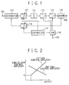
- Fig. 1 shows the configuration of a first embodiment of the gain controller in accordance with the present invention.
- the construction of Fig. 1 includes a distributor 110 which receives an input signal via an input terminal 101 to distribute the signal via two paths to first and second gain control amplifiers 111 and 116.
- the first amplifier 111 produces an output signal to feed the signal via a filter 112 and a driver amplifier 113 to a linear power amplifier 114.
- the signal is amplified by the amplifier 114 to be delivered to a mixer 115.
- the second gain control amplifier 116 creates an output signal to be supplied to the mixer 115. Resultantly, the signal is mixed with the output signal from the linear power amplifier 114 such that a signal resultant from the mixing operation is delivered from an output terminal 102.
- the embodiment includes a power supply 103 producing a voltage signal to be applied via a switching circuit 118 to the linear power amplifier 114, the driver amplifier 113, and the first gain control amplifier 111. Also included in the system is a control circuit 117 which supervises operations of the first and second gain control amplifiers 111 and 116 and the switching circuit 118.
- Fig. 2 shows characteristics of respective amplifiers producing desired outputs when the first and second gain control amplifiers are appropriately controlled.
- the gains respectively of the first and second gain control amplifiers 111 and 116 are set to large and small gain values, respectively. In this situation, primary signals are transmitted via the first path related to the first gain control amplifier 111.
- the relationship above is reversed.
- the switching circuit 118 is activated to conduct a change-over operation so as to turn power of the first amplifier 11, the drive amplifier 113, and the linear power amplifier 114 off. This advantageously reduces current consumption of these circuits substantially to zero.
- the predetermined gain is set to a value sufficiently lower than a level of the distribution path (second path) related to the second gain control amplifier 116, it is possible to minimize influence such as a glitch associated with a power-off operation.
- Fig. 3 shows a second embodiment of the gain controller in accordance with the present invention.
- the same components as those of Fig. 1 are assigned with the same reference numerals and will not be described in this specification.
- the configuration of this embodiment includes a filter 130, an amplifier 131, and an isolator 132 in the distribution path related to the second gain control amplifier 116. Moreover, inserted in the primary path is an isolator 133. There does not occur any trouble even when filter and amplifier functions are added to the distribution path. Depending on an input impedance of the mixer 115, the isolators 132 and 133 may be installed therein to guarantee precision of the output level.
- Fig. 4 shows in a graph an example of relationships of efficiency of the linear power amplifier 114 and the amplifier 131 and input levels respectively thereof.
- the linear power amplifier 114 operates with a high efficiency. Namely, it is possible on this occasion to lower current consumption of the system.
- the relationship above is inverted. That is, current consumption of the system can be minimized by mainly operating the amplifier 131.
- the configuration may includes a plurality of distribution paths.
- the advantageous effect can be similarly obtained through substantially the same control operation of the system.
- there may be arranged an amplifier having optimal efficiency in each distribution path such that efficiency can be controlled more precisely by selectively using the amplifiers.
- the output level for the optimal efficiency varies between these paths. This makes it possible to select one of the paths for the optimal efficiency depending on a desired output value.
- the output level precision can be guaranteed in association with the input impedance of the mixer.
- the control operation can be achieved with a higher precision by increasing the number of paths.
Landscapes
- Engineering & Computer Science (AREA)
- Power Engineering (AREA)
- Amplifiers (AREA)
- Transmitters (AREA)
- Control Of Amplification And Gain Control (AREA)
Applications Claiming Priority (3)
| Application Number | Priority Date | Filing Date | Title |
|---|---|---|---|
| JP103625/97 | 1997-04-21 | ||
| JP10362597A JP3180711B2 (ja) | 1997-04-21 | 1997-04-21 | ゲイン制御装置 |
| JP10362597 | 1997-04-21 |
Publications (3)
| Publication Number | Publication Date |
|---|---|
| EP0876004A2 true EP0876004A2 (fr) | 1998-11-04 |
| EP0876004A3 EP0876004A3 (fr) | 2003-08-20 |
| EP0876004B1 EP0876004B1 (fr) | 2006-01-11 |
Family
ID=14358959
Family Applications (1)
| Application Number | Title | Priority Date | Filing Date |
|---|---|---|---|
| EP98106934A Expired - Lifetime EP0876004B1 (fr) | 1997-04-21 | 1998-04-16 | Dispositif de commande de gain pour un émettteur |
Country Status (5)
| Country | Link |
|---|---|
| US (1) | US6081701A (fr) |
| EP (1) | EP0876004B1 (fr) |
| JP (1) | JP3180711B2 (fr) |
| AU (1) | AU737859B2 (fr) |
| DE (1) | DE69833143T2 (fr) |
Cited By (1)
| Publication number | Priority date | Publication date | Assignee | Title |
|---|---|---|---|---|
| EP1001529A1 (fr) * | 1998-11-10 | 2000-05-17 | Nokia Mobile Phones Ltd. | Montage amplificateur à puissance linéaire et procédé pour sa mise en oeuvre |
Families Citing this family (12)
| Publication number | Priority date | Publication date | Assignee | Title |
|---|---|---|---|---|
| JP3587346B2 (ja) * | 1998-08-07 | 2004-11-10 | 松下電器産業株式会社 | 無線通信装置および無線通信装置における送信電力制御方法 |
| JP3463656B2 (ja) | 2000-07-12 | 2003-11-05 | 日本電気株式会社 | 送信電力増幅装置及びその方法 |
| US7039377B2 (en) * | 2002-06-14 | 2006-05-02 | Skyworks Solutions, Inc. | Switchable gain amplifier |
| WO2004019511A1 (fr) * | 2002-08-21 | 2004-03-04 | Mitsubishi Denki Kabushiki Kaisha | Émetteur radio |
| US7006824B1 (en) | 2002-09-10 | 2006-02-28 | Marvell International Ltd. | Frame/packet-based calibration for wireless transceivers |
| US7215933B1 (en) | 2002-09-24 | 2007-05-08 | Marvell International Ltd. | Local transmitter output power control system for wireless applications |
| US6983135B1 (en) | 2002-11-11 | 2006-01-03 | Marvell International, Ltd. | Mixer gain calibration method and apparatus |
| JP4029086B2 (ja) * | 2004-09-16 | 2008-01-09 | 松下電器産業株式会社 | 送信装置および携帯通信端末装置 |
| KR100716540B1 (ko) | 2005-12-07 | 2007-05-09 | 한국전자통신연구원 | 디지털 자동이득제어 장치 |
| CN101917757B (zh) * | 2010-07-13 | 2013-08-07 | 京信通信系统(中国)有限公司 | 功放管的效率控制方法及其系统和数字射频拉远系统 |
| CN102769463B (zh) * | 2012-08-02 | 2014-08-20 | 中国航天科工集团第二研究院二〇三所 | 一种铯原子频标铯束管微电流信号放大器 |
| JP6078909B2 (ja) * | 2013-03-19 | 2017-02-15 | ジェフコム株式会社 | 切断工具 |
Family Cites Families (20)
| Publication number | Priority date | Publication date | Assignee | Title |
|---|---|---|---|---|
| US3848194A (en) * | 1973-07-16 | 1974-11-12 | Matsushita Electric Co Ltd | Automatic gain control circuit |
| DE3802903A1 (de) * | 1988-02-01 | 1989-08-10 | Siemens Ag | Einrichtung zur uebertragung von sprache |
| JPH01264405A (ja) * | 1988-04-15 | 1989-10-20 | Toshiba Corp | 切換回路 |
| JPH01305610A (ja) * | 1988-06-03 | 1989-12-08 | Hitachi Ltd | 可変利得増幅器 |
| JP2859880B2 (ja) * | 1988-10-07 | 1999-02-24 | 株式会社日立製作所 | 可変利得増幅回路 |
| EP0401771B1 (fr) * | 1989-06-09 | 1995-09-20 | TEMIC TELEFUNKEN microelectronic GmbH | Montage de circuit pour conversion en fréquence |
| JPH04152719A (ja) * | 1990-10-16 | 1992-05-26 | Fujitsu Ltd | 音声検出回路 |
| JP2778260B2 (ja) * | 1991-02-13 | 1998-07-23 | 日本電気株式会社 | 利得制御装置 |
| JP3010404B2 (ja) * | 1993-07-08 | 2000-02-21 | アンリツ株式会社 | 線型回路の利得検出装置および自動利得制御装置 |
| US5432473A (en) * | 1993-07-14 | 1995-07-11 | Nokia Mobile Phones, Limited | Dual mode amplifier with bias control |
| US5561395A (en) * | 1995-01-27 | 1996-10-01 | Motorola, Inc. | Method and apparatus for self-adjusting a multistage radio frequency power amplifier |
| US5514703A (en) * | 1995-03-13 | 1996-05-07 | Eli Lilly And Company | Benzothiophene compounds useful for inhibiting lipoxygenase |
| US5523875A (en) * | 1995-04-24 | 1996-06-04 | Scientific-Atlanta, Inc. | Automatic gain control circuit |
| US5862461A (en) * | 1995-08-31 | 1999-01-19 | Sony Corporation | Transmitting apparatus and method of adjusting gain of signal to be transmitted, and receiving apparatus and method of adjusting gain of received signal |
| JP3772431B2 (ja) * | 1997-01-22 | 2006-05-10 | ソニー株式会社 | 信号処理回路 |
| JP3093638B2 (ja) * | 1996-06-18 | 2000-10-03 | 埼玉日本電気株式会社 | 出力レベル制御回路 |
| FI106413B (fi) * | 1996-07-11 | 2001-01-31 | Nokia Mobile Phones Ltd | Lineaarisen tehovahvistimen tehonsäätöpiiri |
| JPH1032441A (ja) * | 1996-07-15 | 1998-02-03 | Hitachi Denshi Ltd | 電力増幅器 |
| US5862460A (en) * | 1996-09-13 | 1999-01-19 | Motorola, Inc. | Power control circuit for a radio frequency transmitter |
| US5867063A (en) * | 1996-12-05 | 1999-02-02 | Motorola, Inc. | Gain distribution circuit |
-
1997
- 1997-04-21 JP JP10362597A patent/JP3180711B2/ja not_active Expired - Fee Related
-
1998
- 1998-04-15 US US09/060,632 patent/US6081701A/en not_active Expired - Fee Related
- 1998-04-16 EP EP98106934A patent/EP0876004B1/fr not_active Expired - Lifetime
- 1998-04-16 DE DE69833143T patent/DE69833143T2/de not_active Expired - Lifetime
- 1998-04-20 AU AU62821/98A patent/AU737859B2/en not_active Ceased
Cited By (2)
| Publication number | Priority date | Publication date | Assignee | Title |
|---|---|---|---|---|
| EP1001529A1 (fr) * | 1998-11-10 | 2000-05-17 | Nokia Mobile Phones Ltd. | Montage amplificateur à puissance linéaire et procédé pour sa mise en oeuvre |
| US6288606B1 (en) | 1998-11-10 | 2001-09-11 | Nokia Mobile Phones Ltd. | Linear power amplifier arrangement and method for its operation |
Also Published As
| Publication number | Publication date |
|---|---|
| JPH10294626A (ja) | 1998-11-04 |
| JP3180711B2 (ja) | 2001-06-25 |
| US6081701A (en) | 2000-06-27 |
| EP0876004A3 (fr) | 2003-08-20 |
| EP0876004B1 (fr) | 2006-01-11 |
| AU737859B2 (en) | 2001-08-30 |
| AU6282198A (en) | 1998-10-22 |
| DE69833143T2 (de) | 2006-07-06 |
| DE69833143D1 (de) | 2006-04-06 |
Similar Documents
| Publication | Publication Date | Title |
|---|---|---|
| US6081701A (en) | Gain controller | |
| US6782244B2 (en) | Segmented power amplifier and method of control | |
| US6369649B2 (en) | Transmission power amplification method and apparatus | |
| EP0847135A2 (fr) | Dispositif amplificateur haute fréquence à gain variable | |
| US7439809B2 (en) | Radio frequency power amplifier | |
| KR20030013238A (ko) | 피드 포워드 방식 왜곡 보상 증폭 장치 및 어댑티브프리디스토션 방식 왜곡 보상 증폭 장치 | |
| US7190299B2 (en) | Current control method and application thereof | |
| JP3916006B2 (ja) | 無線フロント・エンド回路 | |
| US6057736A (en) | Gain controlled amplifier | |
| US5216378A (en) | Switch adaptable radio frequency amplifier | |
| KR100927650B1 (ko) | 이동통신 단말기용 송신기 및 그것의 송신 방법 | |
| US4631490A (en) | Audio output amplifying device | |
| JP2001274633A (ja) | 電力増幅装置 | |
| JPH09116359A (ja) | 電力増幅回路 | |
| KR100244974B1 (ko) | 스위칭 방식을 적용한 이동 통신 기지국용 저잡음 증폭기 | |
| KR200278532Y1 (ko) | 기준신호를이용한피드포워드증폭기 | |
| US20060068727A1 (en) | Method and system for dynamic range power control | |
| JP3335940B2 (ja) | 送信電力増幅装置 | |
| JPH09266427A (ja) | 多段増幅器 | |
| KR100337528B1 (ko) | 이동통신 단말기의 전력 제어회로 | |
| JPH05335975A (ja) | 無線送信装置 | |
| KR100227782B1 (ko) | 전력증폭기에서 입력 전력에 따른 게이트 전압 제어 회로 | |
| JPS63219215A (ja) | 電力制御装置 | |
| JP4030319B2 (ja) | フィードフォワード非線形歪補償増幅器 | |
| KR100724903B1 (ko) | 부호분할 다중접속 단말기의 이득 조절 장치 |
Legal Events
| Date | Code | Title | Description |
|---|---|---|---|
| PUAI | Public reference made under article 153(3) epc to a published international application that has entered the european phase |
Free format text: ORIGINAL CODE: 0009012 |
|
| AK | Designated contracting states |
Kind code of ref document: A2 Designated state(s): AT BE CH CY DE DK ES FI FR GB GR IE IT LI LU MC NL PT SE |
|
| AX | Request for extension of the european patent |
Free format text: AL;LT;LV;MK;RO;SI |
|
| PUAL | Search report despatched |
Free format text: ORIGINAL CODE: 0009013 |
|
| AK | Designated contracting states |
Designated state(s): AT BE CH CY DE DK ES FI FR GB GR IE IT LI LU MC NL PT SE |
|
| AX | Request for extension of the european patent |
Extension state: AL LT LV MK RO SI |
|
| RIC1 | Information provided on ipc code assigned before grant |
Ipc: 7H 03G 1/00 B Ipc: 7H 03G 3/20 B Ipc: 7H 03F 1/32 B Ipc: 7H 03G 3/32 B Ipc: 7H 04B 1/04 B Ipc: 7H 04B 7/00 A |
|
| 17P | Request for examination filed |
Effective date: 20030714 |
|
| 17Q | First examination report despatched |
Effective date: 20031104 |
|
| AKX | Designation fees paid |
Designated state(s): DE FR GB IT |
|
| GRAP | Despatch of communication of intention to grant a patent |
Free format text: ORIGINAL CODE: EPIDOSNIGR1 |
|
| GRAS | Grant fee paid |
Free format text: ORIGINAL CODE: EPIDOSNIGR3 |
|
| GRAA | (expected) grant |
Free format text: ORIGINAL CODE: 0009210 |
|
| AK | Designated contracting states |
Kind code of ref document: B1 Designated state(s): DE FR GB IT |
|
| REF | Corresponds to: |
Ref document number: 69833143 Country of ref document: DE Date of ref document: 20060406 Kind code of ref document: P |
|
| ET | Fr: translation filed | ||
| PLBE | No opposition filed within time limit |
Free format text: ORIGINAL CODE: 0009261 |
|
| STAA | Information on the status of an ep patent application or granted ep patent |
Free format text: STATUS: NO OPPOSITION FILED WITHIN TIME LIMIT |
|
| 26N | No opposition filed |
Effective date: 20061012 |
|
| PGFP | Annual fee paid to national office [announced via postgrant information from national office to epo] |
Ref country code: GB Payment date: 20100325 Year of fee payment: 13 |
|
| PGFP | Annual fee paid to national office [announced via postgrant information from national office to epo] |
Ref country code: FR Payment date: 20100521 Year of fee payment: 13 |
|
| PGFP | Annual fee paid to national office [announced via postgrant information from national office to epo] |
Ref country code: IT Payment date: 20100419 Year of fee payment: 13 Ref country code: DE Payment date: 20100430 Year of fee payment: 13 |
|
| REG | Reference to a national code |
Ref country code: DE Ref legal event code: R119 Ref document number: 69833143 Country of ref document: DE |
|
| REG | Reference to a national code |
Ref country code: DE Ref legal event code: R119 Ref document number: 69833143 Country of ref document: DE |
|
| GBPC | Gb: european patent ceased through non-payment of renewal fee |
Effective date: 20110416 |
|
| REG | Reference to a national code |
Ref country code: FR Ref legal event code: ST Effective date: 20111230 |
|
| PG25 | Lapsed in a contracting state [announced via postgrant information from national office to epo] |
Ref country code: FR Free format text: LAPSE BECAUSE OF NON-PAYMENT OF DUE FEES Effective date: 20110502 |
|
| PG25 | Lapsed in a contracting state [announced via postgrant information from national office to epo] |
Ref country code: IT Free format text: LAPSE BECAUSE OF NON-PAYMENT OF DUE FEES Effective date: 20110416 Ref country code: GB Free format text: LAPSE BECAUSE OF NON-PAYMENT OF DUE FEES Effective date: 20110416 |
|
| PG25 | Lapsed in a contracting state [announced via postgrant information from national office to epo] |
Ref country code: DE Free format text: LAPSE BECAUSE OF NON-PAYMENT OF DUE FEES Effective date: 20111031 |