EP0880183A2 - LDMOS-Leistungsanordnung - Google Patents
LDMOS-Leistungsanordnung Download PDFInfo
- Publication number
- EP0880183A2 EP0880183A2 EP98201648A EP98201648A EP0880183A2 EP 0880183 A2 EP0880183 A2 EP 0880183A2 EP 98201648 A EP98201648 A EP 98201648A EP 98201648 A EP98201648 A EP 98201648A EP 0880183 A2 EP0880183 A2 EP 0880183A2
- Authority
- EP
- European Patent Office
- Prior art keywords
- region
- rsd
- conductivity type
- transistor
- gate
- Prior art date
- Legal status (The legal status is an assumption and is not a legal conclusion. Google has not performed a legal analysis and makes no representation as to the accuracy of the status listed.)
- Withdrawn
Links
Images

Classifications
-
- H—ELECTRICITY
- H10—SEMICONDUCTOR DEVICES; ELECTRIC SOLID-STATE DEVICES NOT OTHERWISE PROVIDED FOR
- H10D—INORGANIC ELECTRIC SEMICONDUCTOR DEVICES
- H10D30/00—Field-effect transistors [FET]
- H10D30/60—Insulated-gate field-effect transistors [IGFET]
- H10D30/64—Double-diffused metal-oxide semiconductor [DMOS] FETs
- H10D30/65—Lateral DMOS [LDMOS] FETs
-
- H—ELECTRICITY
- H10—SEMICONDUCTOR DEVICES; ELECTRIC SOLID-STATE DEVICES NOT OTHERWISE PROVIDED FOR
- H10D—INORGANIC ELECTRIC SEMICONDUCTOR DEVICES
- H10D30/00—Field-effect transistors [FET]
- H10D30/01—Manufacture or treatment
- H10D30/021—Manufacture or treatment of FETs having insulated gates [IGFET]
- H10D30/028—Manufacture or treatment of FETs having insulated gates [IGFET] of double-diffused metal oxide semiconductor [DMOS] FETs
-
- H—ELECTRICITY
- H10—SEMICONDUCTOR DEVICES; ELECTRIC SOLID-STATE DEVICES NOT OTHERWISE PROVIDED FOR
- H10D—INORGANIC ELECTRIC SEMICONDUCTOR DEVICES
- H10D62/00—Semiconductor bodies, or regions thereof, of devices having potential barriers
- H10D62/10—Shapes, relative sizes or dispositions of the regions of the semiconductor bodies; Shapes of the semiconductor bodies
- H10D62/13—Semiconductor regions connected to electrodes carrying current to be rectified, amplified or switched, e.g. source or drain regions
- H10D62/149—Source or drain regions of field-effect devices
- H10D62/151—Source or drain regions of field-effect devices of IGFETs
- H10D62/156—Drain regions of DMOS transistors
- H10D62/157—Impurity concentrations or distributions
Definitions
- This invention relates to semiconductor devices, and more particularly, to an LDMOS (lateral double-diffused metal oxide semiconductor) device.
- LDMOS lateral double-diffused metal oxide semiconductor
- Battery-operated electronic systems such as notebook personal computers, personal digital assistants, and wireless communication devices often use power MOS (metal oxide semiconductor) devices as low on-resistance electronic switches for distributing battery power.
- MOS metal oxide semiconductor
- low on-resistance can be particularly important to ensure as little power consumption to the battery as possible. This ensures long battery life.
- DMOS devices are "double diffused" MOS devices.
- An DMOS device has a source region and a back gate region, which are diffused at the same time.
- the back gate region is sometimes referred to as a Dwell (double diffused well) region.
- the channel is formed by the difference in the two diffusions, rather than by separate implantation.
- DMOS devices have the advantage of decreasing the length of the channels, thus providing low-power dissipation and high-speed capability.
- DMOS devices may have either lateral or vertical configurations.
- a DMOS device having a lateral configuration (referred to herein as an LDMOS), has its source and drain at the surface of the semiconductor wafer. Thus, the current is lateral. Desired characteristics of an LDMOS are a high breakdown voltage, BV, and a low specific on-resistance.
- One aspect of the invention is an LDMOS transistor having a reduced surface drain (RSD) region.
- the transistor is fabricated on a semiconductor wafer with a first region of a first conductivity type, for example an p type.
- a second region of a second conductivity type, for example an n type, is formed as a well in the first semiconductor region.
- a third region of the first conductivity type is formed as a well in the second region.
- a source region of the second conductivity type is then formed in the third region, drain region of the second conductivity type is formed in the second region and is spaced apart from the source region.
- An RSD region of the second conductivity type is formed in the second region between the source region and the drain region and adjacent to the drain region. This RSD region has a dopant concentration less than that of the drain region. Also, the RSD region is spaced apart from the source region, such that the third region forms a channel between the RSD region and the source region.
- a gate extends over this channel and over at least part of the source region, and at least part of the RSD region.
- a backgate region of the first conductivity type is formed in the third region adjacent to the source region, such that the source region separates the backgate region and the channel.
- the RDS LDMOS transistor of the present invention is well suited for hard disk drive and RF applications. It provides good breakdown voltage characteristics. The process complexity is reduced and thermal stability is good, compared to other LDMOS devices that have attempted to improve breakdown voltage, such as resurface drain extended (RSRF) LDMOS devices.
- RSRF resurface drain extended
- RDS LDMOS devices As compared to shallow Nwell (LV Nwell) LDMOS devices, which are another LDMOS variation, RDS LDMOS devices enable a smaller pitch, using a solid well rather than a donut-shaped well. Its lightly doped drain region is self aligned to the gate polysilicon layer, which ensures process stability. The RSD region allows smaller layer geometry, and offers good conductance at the surface.
- the RSD LDMOS device of the present invention is desirable because of its adherence to the conventional device structure and process. At the same time, it offers good Rsp versus BV performance characteristics.
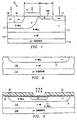
- FIGURE 1 is a cross-sectional elevational view of an reduced surface drain (RSD) LDMOS transistor 10 in accordance with the invention.
- Transistor 10 has a reduced surface drain (RSD) region 15, but is otherwise similar to a planar type LDMOS device.
- a thin oxide layer under gate 14 does not have thick field oxide regions between source regions 16 and drain regions 17 as do non-planer LDMOS devices.
- the RSD region 15 is self aligned to the polysilicon used for gate 14.
- Transistor 10 is formed with an optimized double diffusion for low voltage and is self-isolated by a high-voltage Nwell 12 and the RSD region 15. Additionally, the drain region 17 is spaced back from gate 14. The result is enhanced breakdown voltage, in the range of 15 - 35 volts.
- the RSD region 15 enhances specific ON-resistance (Rsp) as compared to other planar type LDMOS devices.
- the RSD region 15 has good conductance at the surface of transistor 10, providing a lightly doped drain for current flow at the on-state.
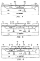
- FIGUREs 2 - 7 are cross-sectional elevational views illustrating successive stages of fabrication of a semiconductor wafer, resulting in a die having numerous transistors 10.
- the fabrication process employs various known semiconductor fabrication techniques, such as photoresist patterning, and the deposition, implantation, and diffusion of various materials.
- the fabrication process is compatible with linear BiCMOS technology such as that developed by Texas Instruments Incorporated.
- photoresist patterning such as the deposition of oxide, nitride, and photoresist layers and their etching and removal, are not completely illustrated. Rather, it is assumed to be understood that these steps are used to provide exposed and masked areas on the surface of the wafer for the purpose of implanting or depositing material in the exposed areas.
- each transistor 10 is built inside a high voltage Nwell.
- the gate oxide (moat) is defined all across the structure. No thick field oxide layers are used inside the device.
- fabrication of a die having transistors 10 begins with the formation of an p-epitaxial layer 11b on a p+ substrate 11a.
- the p+ substrate 11a is typically a heavily doped p+ type silicon that is doped with material of a first conductivity type, such as boron.
- the p-epitaxial layer 11b is typically a lightly doped p-type silicon that is grown by vapor phase epitaxy, liquid metal epitaxy, or other suitable means.
- Oxide and nitride layers are then formed and patterned for implantation of an n-type material, such as phosphorus, antimony, or arsenic. This implant forms Nwell 12.
- the Nwell 12 is then diffused and the oxide and nitride are removed.
- the Nwell 12 is a high voltage, low concentration (n-), deep diffusion well.
- the Nwells 12 provide self-isolation for each transistor 10.
- FIGURE 3 illustrates the formation of Dwells 13.
- a pad oxide layer 31 formed and a photoresist layer 32 is patterned and etched on the surface of the wafer. The pattern is used to expose areas at the surface, which are implanted with p and n type dopants and double-diffused to form low concentration (p-) Dwells 13. Oxide layer 31 and photoresist layer 32 are then removed.
- a threshold adjust layer (p- type) is implanted, resulting in the surface of the Nwell 12 being resistive and resulting in low ON-resistance for transistor 10.
- the Dwell 13 of FIGURE 3 is a "solid" type Dwell. In other embodiments, Dwells 13 could have a “donut” (toroidal) configuration.
- FIGURE 4 illustrates the formation of the gate oxide layer 41 and gates 14.
- An oxide layer 41 is formed and patterned nitride is used to expose areas in which thick field oxide regions and a nitride layer 41a are grown.
- a gate oxide is grown and a polysilicon layer is deposited and etched using patterned photoresist (not shown) to expose certain regions that will become gates 14. The photoresist is then removed, leaving gates 14.
- FIGURE 5 illustrates the formation of the RSD regions 15.
- Appropriate patterning of a photoresist layer 51 is used to mask and expose desired areas on the surface of the wafer.
- the exposed areas are implanted with a shallow co-implant of materials having n type conductivity, specifically, arsenic and phosphorus.
- the "co-implant" is through the same mask, although not necessarily at the same time.
- a typical depth of RSD regions 18 is 0.3 micrometers. No thermal cycle is performed with respect to RSD regions 15.
- the RSD regions 15 provide reduced surface penetration, a reduced surface field adjacent to the gates 14, and reduced surface resistance in the drain region 17.
- FIGURE 6 illustrates sidewalls 14a on gates 14 and the n+ implantation for source regions 16 and drain regions 17. Sidewalls 14a may be formed using conventional sidewall techniques.
- a photoresist layer 61 is patterned and etched, exposing source regions 16 and drain regions 17. These regions are implanted with an n type dopant and diffused, with RSD regions 15 being diffused at the same time.
- the implantation for source regions 16 and drain regions 17 is of higher concentration (n+) than that of RSD regions 15.
- p+ backgate regions 18 are implanted and diffused. These p+ regions 18 are highly concentrated (p+) regions having a depth approximately the same as that of the n+ source regions 16 and drain regions 17. Alternatively, p+ regions 18 may be deeper than the n+ source regions 16 and n+ drain regions 17.
- the RSD layer in the source regions 16 would be performed with a blanket implant of both RSD regions, but would not alter the configuration of FIGURE 1 due to subsequent implantation of the source region 16 and backgate region 18.
- the advantage of this approach is the elimination of a masking step.
- the RSD LDMOS transistor 10 of FIGURE 1 is a portion of the circuitry formed by the process of FIGUREs 2 - 7. Appropriate metallization steps are performed to provide connections and contacts.
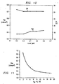
- FIGURE 8 is a graph illustrating Rsp as a function of the length of the resistive path, which is the sum of the distances L (channel length) and Ld (drift length). These distances are illustrated in FIGURE 1.
- Ld is varied, resulting in varying values of Rsp.
- the channel length, L is 1.5 ⁇ m.
- FIGURE 10 is a graph illustrating Rsp and BV as a function of Ld + L, where L is varied.
- the drift length, Ld is 0.8 ⁇ m.
- Vg 10 volts.
- RSD LDMOS transistor 10 favors more L and less Ld because reverse bias depletion extends more into the channel region.
- An optimized performance transistor 10 might have the following operating characteristics:
Landscapes
- Insulated Gate Type Field-Effect Transistor (AREA)
Applications Claiming Priority (2)
| Application Number | Priority Date | Filing Date | Title |
|---|---|---|---|
| US4747497P | 1997-05-23 | 1997-05-23 | |
| US47474P | 1997-05-23 |
Publications (2)
| Publication Number | Publication Date |
|---|---|
| EP0880183A2 true EP0880183A2 (de) | 1998-11-25 |
| EP0880183A3 EP0880183A3 (de) | 1999-07-28 |
Family
ID=21949199
Family Applications (1)
| Application Number | Title | Priority Date | Filing Date |
|---|---|---|---|
| EP98201648A Withdrawn EP0880183A3 (de) | 1997-05-23 | 1998-05-14 | LDMOS-Leistungsanordnung |
Country Status (2)
| Country | Link |
|---|---|
| EP (1) | EP0880183A3 (de) |
| JP (1) | JPH10335663A (de) |
Cited By (7)
| Publication number | Priority date | Publication date | Assignee | Title |
|---|---|---|---|---|
| US6051456A (en) * | 1998-12-21 | 2000-04-18 | Motorola, Inc. | Semiconductor component and method of manufacture |
| US6465839B2 (en) | 2000-04-07 | 2002-10-15 | Denso Corporation | Semiconductor device having lateral MOSFET (LDMOS) |
| US6780697B2 (en) * | 2001-08-21 | 2004-08-24 | Oki Electric Industry Co., Ltd. | Method of manufacturing lateral double-diffused metal oxide semiconductor device |
| EP1779416A4 (de) * | 2004-07-15 | 2009-03-04 | Fairchild Semiconductor | Asymmetrischer hetero-dotierter hochspannungs-mosfet (ah2mos) |
| US8102709B2 (en) | 2009-06-02 | 2012-01-24 | Micron Technology, Inc. | Transistor having peripheral channel |
| US8324042B2 (en) | 2004-07-15 | 2012-12-04 | Fairchild Semiconductor Corporation | Integrated complementary low voltage RF-LDMOS |
| CN106847894A (zh) * | 2015-12-02 | 2017-06-13 | 德克萨斯仪器股份有限公司 | 具有与栅极自对准的体扩散的ldmos器件 |
Families Citing this family (9)
| Publication number | Priority date | Publication date | Assignee | Title |
|---|---|---|---|---|
| KR100341213B1 (ko) * | 1999-12-23 | 2002-06-20 | 오길록 | 트렌치 드레인 구조를 갖는 전력소자 |
| JP3723410B2 (ja) * | 2000-04-13 | 2005-12-07 | 三洋電機株式会社 | 半導体装置とその製造方法 |
| US6787872B2 (en) * | 2001-06-26 | 2004-09-07 | International Rectifier Corporation | Lateral conduction superjunction semiconductor device |
| US6911694B2 (en) | 2001-06-27 | 2005-06-28 | Ricoh Company, Ltd. | Semiconductor device and method for fabricating such device |
| JP4514369B2 (ja) * | 2001-07-19 | 2010-07-28 | 株式会社リコー | 半導体装置及びその製造方法 |
| JP2003115585A (ja) | 2001-10-03 | 2003-04-18 | Oki Electric Ind Co Ltd | 半導体装置の製造方法 |
| US6870218B2 (en) * | 2002-12-10 | 2005-03-22 | Fairchild Semiconductor Corporation | Integrated circuit structure with improved LDMOS design |
| JP4545548B2 (ja) * | 2004-10-21 | 2010-09-15 | ルネサスエレクトロニクス株式会社 | 半導体集積回路及び半導体装置 |
| JP2006245482A (ja) | 2005-03-07 | 2006-09-14 | Ricoh Co Ltd | 半導体装置及びその製造方法、並びにその応用装置 |
Family Cites Families (5)
| Publication number | Priority date | Publication date | Assignee | Title |
|---|---|---|---|---|
| JPS5889866A (ja) * | 1981-11-24 | 1983-05-28 | Hitachi Ltd | 絶縁ゲ−ト半導体装置 |
| JP2545762B2 (ja) * | 1990-04-13 | 1996-10-23 | 日本電装株式会社 | 高耐圧misトランジスタおよびこのトランジスタを有する相補型トランジスタの製造方法 |
| JP3186421B2 (ja) * | 1994-05-13 | 2001-07-11 | 富士電機株式会社 | 半導体装置の製造方法 |
| US5517046A (en) * | 1993-11-19 | 1996-05-14 | Micrel, Incorporated | High voltage lateral DMOS device with enhanced drift region |
| US5719423A (en) * | 1995-08-31 | 1998-02-17 | Texas Instruments Incorporated | Isolated power transistor |
-
1998
- 1998-05-14 EP EP98201648A patent/EP0880183A3/de not_active Withdrawn
- 1998-05-22 JP JP10140692A patent/JPH10335663A/ja active Pending
Cited By (11)
| Publication number | Priority date | Publication date | Assignee | Title |
|---|---|---|---|---|
| US6051456A (en) * | 1998-12-21 | 2000-04-18 | Motorola, Inc. | Semiconductor component and method of manufacture |
| US6153905A (en) * | 1998-12-21 | 2000-11-28 | Motorola, Inc. | Semiconductor component including MOSFET with asymmetric gate electrode where the drain electrode over portions of the lightly doped diffusion region without a gate dielectric |
| US6465839B2 (en) | 2000-04-07 | 2002-10-15 | Denso Corporation | Semiconductor device having lateral MOSFET (LDMOS) |
| US6573144B2 (en) | 2000-04-07 | 2003-06-03 | Shigeki Takahashi | Method for manufacturing a semiconductor device having lateral MOSFET (LDMOS) |
| US6780697B2 (en) * | 2001-08-21 | 2004-08-24 | Oki Electric Industry Co., Ltd. | Method of manufacturing lateral double-diffused metal oxide semiconductor device |
| EP1779416A4 (de) * | 2004-07-15 | 2009-03-04 | Fairchild Semiconductor | Asymmetrischer hetero-dotierter hochspannungs-mosfet (ah2mos) |
| US7649225B2 (en) | 2004-07-15 | 2010-01-19 | Fairchild Semiconductor Corporation | Asymmetric hetero-doped high-voltage MOSFET (AH2MOS) |
| US8324042B2 (en) | 2004-07-15 | 2012-12-04 | Fairchild Semiconductor Corporation | Integrated complementary low voltage RF-LDMOS |
| US8102709B2 (en) | 2009-06-02 | 2012-01-24 | Micron Technology, Inc. | Transistor having peripheral channel |
| CN106847894A (zh) * | 2015-12-02 | 2017-06-13 | 德克萨斯仪器股份有限公司 | 具有与栅极自对准的体扩散的ldmos器件 |
| CN106847894B (zh) * | 2015-12-02 | 2021-07-09 | 德克萨斯仪器股份有限公司 | 具有与栅极自对准的体扩散的ldmos器件 |
Also Published As
| Publication number | Publication date |
|---|---|
| EP0880183A3 (de) | 1999-07-28 |
| JPH10335663A (ja) | 1998-12-18 |
Similar Documents
| Publication | Publication Date | Title |
|---|---|---|
| US7608512B2 (en) | Integrated circuit structure with improved LDMOS design | |
| US6518138B2 (en) | Method of forming Self-aligned lateral DMOS with spacer drift region | |
| KR100468342B1 (ko) | 자기-정렬resurf영역을가진ldmos장치및그제조방법 | |
| KR0167273B1 (ko) | 고전압 모스전계효과트렌지스터의 구조 및 그 제조방법 | |
| US5406110A (en) | Resurf lateral double diffused insulated gate field effect transistor | |
| US6531355B2 (en) | LDMOS device with self-aligned RESURF region and method of fabrication | |
| US5346835A (en) | Triple diffused lateral resurf insulated gate field effect transistor compatible with process and method | |
| US6084268A (en) | Power MOSFET device having low on-resistance and method | |
| US6551870B1 (en) | Method of fabricating ultra shallow junction CMOS transistors with nitride disposable spacer | |
| US6555872B1 (en) | Trench gate fermi-threshold field effect transistors | |
| US8916929B2 (en) | MOSFET having a JFET embedded as a body diode | |
| US5736766A (en) | Medium voltage LDMOS device and method of fabrication | |
| US6614075B2 (en) | Semiconductor device and method of manufacturing the same | |
| EP0718892B1 (de) | Halbleiterbauelement mit Bipolartransistor mit isolierter Gateelektrode und dessen Herstellungsverfahren | |
| EP0880183A2 (de) | LDMOS-Leistungsanordnung | |
| JP2008514007A (ja) | スタック状ヘテロドーピング周縁部及び徐々に変化するドリフト領域を備えた促進された表面電界低減化高耐圧p型mosデバイス | |
| KR100611111B1 (ko) | 고주파용 모오스 트랜지스터, 이의 형성 방법 및 반도체장치의 제조 방법 | |
| US6194760B1 (en) | Double-diffused MOS transistor and method of fabricating the same | |
| CN100459073C (zh) | 横向双扩散金属氧化物半导体元件及其制造方法 | |
| KR100281397B1 (ko) | 초박형 soi 정전기방전 보호 소자의 형성 방법 | |
| US6882013B2 (en) | Transistor with reduced short channel effects and method | |
| JPH08236757A (ja) | Ldmos装置 | |
| US7335549B2 (en) | Semiconductor device and method for fabricating the same | |
| KR100521994B1 (ko) | 트렌치게이트형모스트랜지스터및그제조방법 | |
| KR0165347B1 (ko) | 고내압 트랜지스터 및 그 제조방법 |
Legal Events
| Date | Code | Title | Description |
|---|---|---|---|
| PUAI | Public reference made under article 153(3) epc to a published international application that has entered the european phase |
Free format text: ORIGINAL CODE: 0009012 |
|
| AK | Designated contracting states |
Kind code of ref document: A2 Designated state(s): DE FR GB IT NL |
|
| AX | Request for extension of the european patent |
Free format text: AL;LT;LV;MK;RO;SI |
|
| PUAL | Search report despatched |
Free format text: ORIGINAL CODE: 0009013 |
|
| AK | Designated contracting states |
Kind code of ref document: A3 Designated state(s): AT BE CH CY DE DK ES FI FR GB GR IE IT LI LU MC NL PT SE |
|
| AX | Request for extension of the european patent |
Free format text: AL;LT;LV;MK;RO;SI |
|
| 17P | Request for examination filed |
Effective date: 20000128 |
|
| AKX | Designation fees paid |
Free format text: DE FR GB IT NL |
|
| 17Q | First examination report despatched |
Effective date: 20070911 |
|
| STAA | Information on the status of an ep patent application or granted ep patent |
Free format text: STATUS: THE APPLICATION IS DEEMED TO BE WITHDRAWN |
|
| 18D | Application deemed to be withdrawn |
Effective date: 20080326 |