EP0882818B1 - Verfahren zur Herstellung Siliziumkristallen - Google Patents
Verfahren zur Herstellung Siliziumkristallen Download PDFInfo
- Publication number
- EP0882818B1 EP0882818B1 EP98110324A EP98110324A EP0882818B1 EP 0882818 B1 EP0882818 B1 EP 0882818B1 EP 98110324 A EP98110324 A EP 98110324A EP 98110324 A EP98110324 A EP 98110324A EP 0882818 B1 EP0882818 B1 EP 0882818B1
- Authority
- EP
- European Patent Office
- Prior art keywords
- silicon
- germanium
- melt
- crystal
- melt layer
- Prior art date
- Legal status (The legal status is an assumption and is not a legal conclusion. Google has not performed a legal analysis and makes no representation as to the accuracy of the status listed.)
- Expired - Lifetime
Links
Images

Classifications
-
- C—CHEMISTRY; METALLURGY
- C30—CRYSTAL GROWTH
- C30B—SINGLE-CRYSTAL GROWTH; UNIDIRECTIONAL SOLIDIFICATION OF EUTECTIC MATERIAL OR UNIDIRECTIONAL DEMIXING OF EUTECTOID MATERIAL; REFINING BY ZONE-MELTING OF MATERIAL; PRODUCTION OF A HOMOGENEOUS POLYCRYSTALLINE MATERIAL WITH DEFINED STRUCTURE; SINGLE CRYSTALS OR HOMOGENEOUS POLYCRYSTALLINE MATERIAL WITH DEFINED STRUCTURE; AFTER-TREATMENT OF SINGLE CRYSTALS OR A HOMOGENEOUS POLYCRYSTALLINE MATERIAL WITH DEFINED STRUCTURE; APPARATUS THEREFOR
- C30B29/00—Single crystals or homogeneous polycrystalline material with defined structure characterised by the material or by their shape
- C30B29/02—Elements
- C30B29/06—Silicon
-
- C—CHEMISTRY; METALLURGY
- C30—CRYSTAL GROWTH
- C30B—SINGLE-CRYSTAL GROWTH; UNIDIRECTIONAL SOLIDIFICATION OF EUTECTIC MATERIAL OR UNIDIRECTIONAL DEMIXING OF EUTECTOID MATERIAL; REFINING BY ZONE-MELTING OF MATERIAL; PRODUCTION OF A HOMOGENEOUS POLYCRYSTALLINE MATERIAL WITH DEFINED STRUCTURE; SINGLE CRYSTALS OR HOMOGENEOUS POLYCRYSTALLINE MATERIAL WITH DEFINED STRUCTURE; AFTER-TREATMENT OF SINGLE CRYSTALS OR A HOMOGENEOUS POLYCRYSTALLINE MATERIAL WITH DEFINED STRUCTURE; APPARATUS THEREFOR
- C30B11/00—Single-crystal growth by normal freezing or freezing under temperature gradient, e.g. Bridgman-Stockbarger method
-
- C—CHEMISTRY; METALLURGY
- C30—CRYSTAL GROWTH
- C30B—SINGLE-CRYSTAL GROWTH; UNIDIRECTIONAL SOLIDIFICATION OF EUTECTIC MATERIAL OR UNIDIRECTIONAL DEMIXING OF EUTECTOID MATERIAL; REFINING BY ZONE-MELTING OF MATERIAL; PRODUCTION OF A HOMOGENEOUS POLYCRYSTALLINE MATERIAL WITH DEFINED STRUCTURE; SINGLE CRYSTALS OR HOMOGENEOUS POLYCRYSTALLINE MATERIAL WITH DEFINED STRUCTURE; AFTER-TREATMENT OF SINGLE CRYSTALS OR A HOMOGENEOUS POLYCRYSTALLINE MATERIAL WITH DEFINED STRUCTURE; APPARATUS THEREFOR
- C30B15/00—Single-crystal growth by pulling from a melt, e.g. Czochralski method
Definitions
- the present invention relates to a method for manufacturing silicon crystal.
- Silicon crystals include single crystalline silicon and polycrystalline silicon.
- the single crystalline silicon is used as a starting material for manufacturing a semiconductor device such as LSI.
- LSI semiconductor device
- the single crystalline silicon is generally manufactured by use of a CZ type crystal growing device (e.g. EP-A-0 499 471) or FZ type crystal growing device.
- the CZ type crystal growing device is a device most frequently used for the manufacture of single crystalline silicon. This device generally has a structure in which starting polycrystalline silicon is put into a quartz glass crucible followed by melting, and the resulting single crystalline silicon is lifted up from the melt surface.
- a carbon heating element is used, and the silicon is melted by indirect heating from the circumference of the crucible.
- a carbon-made holder is arranged on the outside of the quartz glass crucible in order to keep the shape.
- the quartz crucible is heated to a temperature equal to or higher than the melting point (1413 °C) of silicon. Therefore, silicon dioxide of which the quartz glass crucible is composed is eluted into the silicon melt, resulting in the incorporation of oxygen into the single crystalline silicon to be lifted up.
- the oxygen contained in the single crystalline silicon often effectively acts in the manufacturing process of a device to achieve intrinsic gettering function or the like, but disadvantageously increases crystal defects in a silicon wafer when a large quantity is contained.
- the general FZ type crystal growing device adapts a method of passing a polycrystalline silicon preliminarily formed in bar into a high frequency coil having an inside diameter of several centimeters from above, and locally heating and melting it to grow the single crystalline silicon downward.
- the melt part does not directly make contact with the quartz glass member, the oxygen incorporated into the crystal can be extremely minimized.
- the oxygen concentration in the single crystalline silicon could not be sufficiently reduced in the CZ type crystal growing device.
- the heating temperature had to be raised since the quartz crucible is enlarged. Therefore, the deformation of the -crucible and the elution of silicon dioxide from the crucible wall were increased, and a large quantity of oxygen was incorporated into the crystal, which had a significant influence on the quality of the single crystalline silicon.
- the FZ type crystal growing device can control the oxygen concentration to a low level.
- the diameter of the to be single crystalline silicon grown was limited in the FZ type crystal growing device, and a single crystalline silicon with large diameter could not be manufactured.
- the present invention has an object to provide a method for manufacturing silicon crystal in which the oxygen concentration in the crystal can be reduced, and the diameter can be also enlarged.
- a germanium melt layer is interposed between solid silicon raw material and silicon crystal to be grown. Further, a silicon melt layer may be formed between the germanium melt layer and the silicon crystal.
- the silicon melt can be kept in the melt state at a temperature lower than the melting point of silicon to manufacture the silicon crystal from this melt.
- the silicon crystal can be manufactured by melting solid silicon by heating in a temperature range of 1000-1400°C which is lower than 1413 °C of the melting point of silicon. Therefore, the eluting quantity of a quartz member for holding the melt can be decreased to reduce the oxygen concentration incorporated into the silicon crystal. Further, the damage of a member for supporting the melt can be also reduced.
- At least the germanium melt layer is heated to a temperature of 1000-1400°C.
- heating is performed with a temperature gradient between the upper and lower part of the germanium melt layer.
- the thickness of the germanium melt layer is set to 5 mm-100 mm.
- the single crystalline silicon can be lifted up from the silicon melt layer by use of a seed crystal.
- the silicon melt is passed through the germanium melt layer to recrystallize silicon (18), whereby oxygen concentration is reduced.
- the oxygen concentration in the single crystalline silicon and silicon polycrystal manufactured by the present invention can be reduced to 1 ⁇ 10 16 atoms/cm 3 or more and less than 1 ⁇ 10 18 atoms/cm 3 .
- the germanium content in the silicon crystal can be similarly reduced to 0.5-1 atoms %.
- a device for manufacturing silicon crystal comprises a holding means for holding a germanium melt layer on the upper part of solid silicon raw material and a heater for heating it provided on the outside of the holding means, so that the silicon is recrystallized through the germanium melt layer to grow the silicon crystal.
- the heater can be constituted so as-to heat with a temperature gradient in the axial direction of the holding means.
- the solid silicon raw material can be continuously supplied from the bottom part of the holding means.
- the holding means can be constituted so as to hold the recrystallized silicon polycrystal.
- a lifting means can be provided above the holding means.
- a seed crystal formed of single crystalline silicon is provided on the end part of the lifting means, and this is brought into contact with the silicon melt layer to continuously recrystallize the silicon melt, whereby the single crystalline silicon can be manufactured.
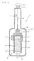
- Fig. 1 is a sectional view showing a first embodiment of the present invention.
- Fig. 2 is a sectional view showing a second embodiment of the present invention.
- Fig. 3 is a partially perspective view showing a third embodiment of the present invention.
- Fig. 4 is a view illustrating a manufacturing process in the manufacturing device of Fig. 3.
- Fig. 5 is a sectional view showing an application of the present invention.
- the most important technical item in the method for manufacturing silicon crystal of the present invention is to bring germanium melt into contact with a solid silicon raw material.
- the melting point of germanium is 936 °C.
- the melting point of silicon is 1413°C as is known (it varies with literature, and is generally described as 1410-1414 °C).
- the above-mentioned phenomenon occurs when the temperature of the germanium melt, more specifically, the temperature of the contact critical surface between the germanium and the solid silicon is equal to or higher than 1000°C and lower than 1413°C.
- the solid silicon can not be melted into germanium.
- the silicon starts to melt when the temperature exceeds 1000 °C the silicon does not come to float on the germanium mel t, since it is dissolved into germanium in the initial stage of melting as described below.
- the practically usable temperature range is 1150 °C or higher and lower than 1350°C.
- the solid silicon raw material melts into the ger manium melt at a sufficient speed, quickly reaches the above saturated state, and then forms a silicon melt layer on the upper part of the germanium melt layer.
- a temperature equal to or higher than 1350 °C which is close to the melting point of sili con.
- various effects of the formation of the silicon melt layer at a temperature lower than the melting point of silicon according to the present invention are reduced.
- the solid silicon raw material may be in any crystalline state, or may be amorphous.
- the floated silicon melt keeps the melt state in spite of the temperature lower than the melting point of silicon.
- the thickness of the silicon melt layer capable of keeping the melt state varies depending on the thermal environment around it, it is on the order of several mm when the temperature in and around the germanium melt is kept in soaking state at 1200°C.
- the silicon melt is continuously floated through the germanium melt, the quantity of the silicon present on the germa nium melt is increased to thicken the melt layer. At a result, recrystallization is started in the part distant from the germanium melt.
- the germanium melt of a prescribed temperature When the germanium melt of a prescribed temperature is continuously brought into contact with the solid silicon, thus, the silicon crystal recrystallized on the germanium melt layer can be continuously formed.
- the cooling speed of the silicon melt is regulated at that time, whereby a polycrystalline silicon formed of dendrite type crystal grain having a grain size of 300 ⁇ m-15 mm can be manufactured.
- the single crystalline silicon can be lifted up from the silicon melt layer by use of a seed crystal in the same manner as the known CZ method.
- the dissolving of silicon into germanium melt is about 40 atoms % at 1200°C.
- the silicon from the solid silicon raw material is dissolved into the germanium melt until it reaches this composition, so that it does not come to float onto the upper part of the germanium melt to form the silicon melt layer. After it reaches this composition, excessive silicon is floated on the germanium melt to form the silicon melt layer.
- germanium is slightly contained in this silicon melt layer, the solid solubility with germanium of the silicon is extremely small, and the quantity of germanium incorporated into the recrystallized silicon crystal is about 0.5-1 atoms %.
- the thickness of the germanium melt layer can be set to 5-100 mm.
- the more preferable thickness is 5-30 mm.
- the germanium melt With a thickness less than 5 mm, the germanium melt might be coagulated in droplet, because of its large surface tension, so that no "layer" can be formed.
- the convention in the germanium melt might be increased to make it difficult to form a stable silicon melt layer.
- the silicon dissolved into the germanium melt is considered to be mutually collected to form an assembly while it is perfectly dissolved and floated by the density difference.
- This assembly is coalesced with the silicon melt layer when it reaches the surface layer of the germanium melt.
- the germanium melt layer is preferably thinned so that no assembly is formed, or the assembly is not enlarged in order to minimize the influence in the coalescence of the assembly with the silicon melt layer.
- the temperature gradient of germanium melt layer-silicon melt layer-recrystallized silicon polycrystal determines the size of the dendrite type silicon crystal grain in the polycrystal to be grown.
- the size of the crystal grain is increased.
- the temperature of the germanium melt is high. the quantity of the silicon to be floated is increased to thicken the melt layer, and the distant part is forcedly crystallized (because the temperature of the whole melt is lower than the melting point). Therefore, the crystallizing speed is raised, and the size of the crystal grain is apt to be small. Accordingly, the size of crystal grain can be controlled by controlling the germanium melt temperature and the temperature gradient.
- the silicon dissolved in the bottom part is solidified in the course of floating in the germanium melt layer, and floated as a solid dendrite type silicon crystal grain onto the germanium melt layer surface.
- the thickness of the germanium melt layer and the temperature gradient are controlled, whereby a silicon crystal having a size of about 300 ⁇ m-15 mm can be provided. Since it becomes difficult to give a desired temperature gradient when a conv ection is generated within the germanium melt layer, a control such as addition of a magnetic field to suppress the convection is required.
- the silicon melt can be formed at a low temperature lower than the melting point of silicon to recrystallize silicon.
- the viscosity of the crucible can be kept high because of the low temperature even if a quartz glass-made material is used as the holding member of germanium and silicon melts, the silicon dioxide melted into the melt is minimized, and the oxygen concentration in the silicon crystal can be consequently reduced to about 1/100-1/1000 in the general CZ method.
- a silicon crystal having an oxygen concentration of 1 ⁇ 10 16 atoms/cm 3 or more and less than 1 ⁇ 10 18 atoms/cm 3 can be manufactured.
- a silicon crystal having a germanium content of 0.5-1 atoms % can be manufactured.
- the electron and Hall mobilities can be significantly increased, compared with a conventional one.
- the germanium melt layer and the upper and lower areas thereof can be heated.
- the solid silicon raw material can be heated only in the adjacent part with the germanium melt layer.
- Fig. 1 is a sectional view showing a first embodiment of a device for manufacturing silicon crystal according to the present invention.
- a single crystalline silicon manufacturing device 1 has a water-cooled chamber 11, and a single crystalline silicon lifting means 12 is arranged on the upper part thereon.
- the single crystalline silicon lifting means 12 is constituted so as to lift up a silicon crystal with rotation by a wire 13 having a seed crystal attached on the end thereof (referred to arrows (b) and (c)).
- a holding means 10 for holding a mass of starting polycrystalline silicon 18 and germanium melt 19 is arranged within the water-cooled chamber 11.
- the holding means 10 is formed of a tubular high purity quartz glass member 14, a high purity carbon-made holding member 15 forming an outer tube, and a bottom member 16 forming a bottom wall.
- the bottom member 16 is supported by a shaft integrally fixed thereto in such a manner as to be vertically movable.
- a carbon felt or the like can be interposed between the starting polycrystalline silicon 18 and the quartz glass tube 14. Since the germanium is not wetted by carbon at all, the germanium melt is never penetrated into the carbon felt. Thus. the starting silicon 18 can be pressed up by the bottom member 16. The above structure is preferred for the continuous supply of the silicon raw material.
- the thicknesses of the quartz glass member 14 and the carbon member 15 supporting it can be reduced, compared with the thicknesses of a quartz glass crucible and carbon-made holding member (carbon crucible) used in the conventional CZ method.
- the reason for this is that the heating temperature in the execution of the present invention can be set to not a temperature equal to or higher than 1413°C of the melting point of silicon which is adapted in the conventional CZ method, but about 1000-1400°C close to the melting point of germanium, preferably 1150-1350°C.
- a heating high frequency coil 17 is arranged on the circumference of the tubular support means 10 so as to heat a relatively narrow axial range.
- the high frequency coil 17 is vertically movable as shown by an arrow (a).
- the high frequency coil 17 is moved so as to heat, centered with respect to the germanium melt layer 19, the upper layer part of the starting polycrystalline silicon 18 on the lower side and a silicon melt 21 on the upper side as shown in the drawing.
- the high frequency coil 17 can not be moved.
- the high frequency coil 17 can be constituted so as to heat with a temperature gradient. It may have a structure separated into several heat zones.
- the starting polycrystalline silicon 18 is put into the cylindrical support means 10, and germanium is arranged thereon.
- the chamber is kept in vacuum inert gas atmosphere.
- a power is applied to the high frequency coil 17 to make the carbon member 15 generate a heat, and the germanium and the periphery thereof are heated to about 1000-1350 °C to melt the germanium, whereby a germanium melt layer 19 is formed.
- the starting polycrystalline silicon 18 in the boundary area is melted into the germanium melt layer 19 regardless of the temperature lower than the melting point of silicon, and floated on the germanium melt layer 19 by the density difference with germanium to form a silicon layer 21.
- the single crystalline silicon 20 is lifted up from the silicon layer 21 in the same manner as the general CZ method by the single crystalline silicon lifting means 12.
- the quantity of the germanium incorporated into the grown silicon crystal is about 0.5-1 atoms %.
- the silicon layer formed on the germanium melt layer 19 is kept at a temperature lower than the general melting point. Since only the narrow range of the germanium melt layer 19 and the periphery thereof is heated, the power consumption can be significantly reduced, compared with a conventional CZ furnace. The damage to the quartz glass member 15 contact with the melt is also minimized because of the low temperature. Further, the oxygen quantity incorporated into the single crystalline silicon can be also significantly reduced since the quantity of the silicon dioxide eluted to the melt is remarkably reduced.
- a quartz glass tube with an inside diameter of 200 mm and a length of 400 mm was used as the quartz glass-made tubular member, and a high purity carbon member was used as the outer tube.
- a cylindrical starting polycrystalline silicon (about 22 Kg) having a diameter of 200 mm and a height of 300 mm was put into the quartz glass tube, 1 Kg of germanium was arranged thereon, and the starting material upper part and germanium were heated. When it was successively heated to 1200°C, germanium was perfectly melted to form a layer in a thickness of about 6 mm on the upper part of the silicon starting material, and a silicon melt layer was formed on the upper part thereof.
- a seed crystal was brought into contact with the silicon melt layer to lift up a single crystalline silicon about 70 mm in diameter. The furnace temperature in silicon melting start, the crystal growing melt holding surface temperature, and the oxygen quantity in the resulting single crystalline silicon were measured. The results are shown in the column of Example (silicon + germanium) of Table 1.
- the single crystalline silicon could be manufactured at a temperature lower than the melting point according to the conventional CZ method by about 200 °C in the Example (silicon + germanium) of the present invention.
- the ox ygen quantity incorporated into the single crystalline silicon could be also reduced to 1/100-1/1000 in the conventional CZ method.
- a single crystalline silicon manufacturing device 3 has a water-cooled chamber 31.
- a holding means 30 for holding a mass of starting polycrystalline silicon 18 and germanium melt 19 is arranged within the water-cooled chamber 31.
- the holding means 30 is formed of a tubular high purity quartz glass member 34, a high purity carbon-made holding member 35 forming an outer tube, and a bottom member 36 forming a bottom wall.
- the bottom member 36 is supported by a shaft integrally fixed thereto in such a manner as to be vertically movable.
- the thickness of the quartz glass member 34 and the carbon member 35 for supporting it can be reduced, compared with the thickness of the quartz glass crucible and carbon-made holding member (carbon crucible) used in conventional CZ method.
- the reason for this is that the heating temperature in the execution of the present invention can be set to not a temperature equal to or high than 1413°C of the melting point of silicon which is adapted in the conventional CZ method, but a temperature of about 1000-1400 °C which is close to the melting point of germanium, preferably 1150-1350 °C.
- a heating high frequency coil 37 is arranged on the circumference of the tubular support means 30 so as to heat a relatively narrow axial range.
- the high frequency coil 37 is vertically movable as shown by an arrow (a).
- the high frequency coil 37 is moved so as to heat, centered with respect to the germanium melt layer 19, the upper part of the starting polycrystalline silicon 18 and the silicon melt 21 on the upper side thereof, as shown in the drawing.
- the high frequency coil 37 can not be moved.
- the high frequency coil 37 can be constituted so as to heat with a temperature gradient. It may have a structure separated into several heat zones.
- the starting polycrystalline silicon 18 is put in the cylindrical support means 30, and germanium is arranged thereon.
- the chamber is kept under vacuum inert gas atmosphere.
- a power is applied to the high frequency coil 37 to make the carbon member 35 generate a heat, and the germanium and the periphery thereof are heated to about 1000-1350 °C to melt the germanium, whereby a germanium melt layer 19 is formed.
- the starting polycrystalline silicon 18 in the boundary area is dissolved into the germanium melt layer 19 regardless of the temperature lower than the melting point of silicon, and floated on the upper part of the germanium melt layer 19 by the density difference with germanium to form the silicon layer 21.
- the quantity of the germanium incorporated into the grown silicon crystal is about 0.5-1 atoms %.
- the silicon layer formed on the germanium melt layer 19 is kept at a temperature lower than the general melting point. Since only the narrow range of the germanium melt layer 19 and the periphery thereof is heated, the power consumption can be significantly reduced, compared with a conventional CZ furnace. The damage to the quartz glass member 15 contact with the melt is also minimized because of the low temperature. Further, the oxygen quantity incorporated into the silicon crystal can be also significantly reduced since the quantity of the silicon dioxide eluted into the melt is remarkably reduced.
- a quartz glass tube having an inside diameter of 200 mm and a length of 600 mm was used as the quartz glass-made tubular member, and a high purity carbon member was used as the outer tube.
- a cylindrical starting polycrystalline silicon (about 33 Kg) having a diameter of 200 mm and a height of 450 mm was put into the quartz glass tube, 2 Kg of germanium was arranged thereon, and the starting material upper part and the germanium were heated. When they were heated to 1200 °C, it was confirmed that the germanium was perfectly melted to form a layer in a thickness of about 12 mm on the upper part of the silicon starting material, and a silicon melt layer was formed on the upper part thereof.
- This polycrystal had a general dendrite type crystalline structure.
- the high frequency coil 37 was moved so as to situate the germanium layer in the center during the manufacture.
- the size of one dendrite type crystal unit constituting the polycrystalline silicon 22 is 3-5 mm under the environment where the silicon crystal is gradually cooled at a speed of 50-200 °C /hour.
- the outside of the recrystallized polycrystalline silicon 22 is supported by the holding means 30 so as to be cylindrically grown.
- a large polycrystalline silicon of dendrite type crystal is useful for the application to a solar battery or the like.
- Fig. 3 shows a polycrystalline silicon manufacturing device 4 which is a third embodiment for conducting the present invention.
- a support means 41 is set within a chamber not shown, and kept in argon atmosphere.
- the support means 41 has a rectangular shallow box shape so as to manufacture a polycrystalline silicon sheet.
- Fig. 4 shows a process of manufacturing a polycrystalline silicon sheet, wherein (A) shows the state before heating, and (B) shows the state after heating.
- a heating is performed by use of a heater not shown so as to impart a temperature gradient (the temperature is high in the lower part and low in the upper part) shown by an arrow (d) in Fig. 4(B), whereby a polycrystalline silicon sheet 23 is grown on the upper surface of a germanium melt 19.
- the temperature gradient is set to, for example, about 0.2-1.00 °C /mm.
- a thin plate-like silicon polycrystal can be directly provided, and the process of slicing can be omitted in the application to solar battery or the like.
- the germanium melt is interposed between the solid silicon starting material and the silicon melt according to the present invention, the silicon crystal can be developed at a temperature greatly lower than the melting point of silicon.
- the base liquid temperature for growing the silicon crystal can be lowered, the oxygen incorporated into the melt from the support member (crucible or the like) contact with the silicon fused solution, and, in its turn, into the silicon crystal can be significantly reduced, and the durable life of the support member can be remarkably improved. Further, the energy required for the manufacture of silicon crystal can be also significantly reduced.
- the present invention is never limited by the embodiments described above.
- a polycrystalline silicon according to this shape can be grown.
- a heater other than high frequency heater for example, a carbon-made resistant heating heater or the like can be used.
Landscapes
- Chemical & Material Sciences (AREA)
- Engineering & Computer Science (AREA)
- Crystallography & Structural Chemistry (AREA)
- Materials Engineering (AREA)
- Metallurgy (AREA)
- Organic Chemistry (AREA)
- Crystals, And After-Treatments Of Crystals (AREA)
- Liquid Deposition Of Substances Of Which Semiconductor Devices Are Composed (AREA)
Claims (7)
- Verfahren zum Herstellen von Siliziumkristall, gekennzeichnet durch den Schritt, eine Germaniumschmelzschicht (19) zwischen festem Siliziumausgangsmaterial (18) und zu wachsendem Siliziumkristall (20, 22, 23) anzuordnen.
- Verfahren nach Anspruch 1, dadurch gekennzeichnet, daß eine Siliziumschmelzschicht (21) zwischen der Germaniumschmelzschicht (19) und dem Siliziumkristall (20) ausgebildet wird.
- Verfahren nach Anspruch 2, dadurch gekennzeichnet, daß die Temperatur der Siliziumschmelzschicht (21) niedriger ist als der Schmelzpunkt von Silizium.
- Verfahren nach einem der Ansprüche 1 bis 3, dadurch gekennzeichnet, daß wenigstens die Germaniumschmelzschicht (19) auf eine Temperatur von 1000 bis 1400°C erwärmt wird.
- Verfahren nach einem der Ansprüche 1 bis 4, dadurch gekennzeichnet, daß die Dicke der Germaniumschmelzschicht (19) eingestellt wird auf 5 bis 100 mm.
- Verfahren nach einem der Ansprüche 1 bis 5, dadurch gekennzeichnet, daß eine Erwärmung durchgeführt wird, um zwischen dem oberen und dem unteren Teil der Germaniumschmelzschicht (19) einen Temperaturgradienten zu erzeugen.
- Verfahren nach einem der Ansprüche 2 bis 6, dadurch gekennzeichnet, daß ein Einkristallsilizium (20) aus der Siliziumschmelzschicht durch Verwendung eines Keimkristalls nach oben gezogen wird.
Applications Claiming Priority (3)
| Application Number | Priority Date | Filing Date | Title |
|---|---|---|---|
| JP16356297 | 1997-06-06 | ||
| JP163562/97 | 1997-06-06 | ||
| JP16356297 | 1997-06-06 |
Publications (2)
| Publication Number | Publication Date |
|---|---|
| EP0882818A1 EP0882818A1 (de) | 1998-12-09 |
| EP0882818B1 true EP0882818B1 (de) | 2000-12-06 |
Family
ID=15776270
Family Applications (1)
| Application Number | Title | Priority Date | Filing Date |
|---|---|---|---|
| EP98110324A Expired - Lifetime EP0882818B1 (de) | 1997-06-06 | 1998-06-05 | Verfahren zur Herstellung Siliziumkristallen |
Country Status (4)
| Country | Link |
|---|---|
| US (1) | US6096128A (de) |
| EP (1) | EP0882818B1 (de) |
| KR (1) | KR100304291B1 (de) |
| DE (1) | DE69800420T2 (de) |
Families Citing this family (2)
| Publication number | Priority date | Publication date | Assignee | Title |
|---|---|---|---|---|
| US6632280B2 (en) * | 2000-01-31 | 2003-10-14 | Shin-Etsu Handotai Co., Ltd. | Apparatus for growing single crystal, method for producing single crystal utilizing the apparatus and single crystal |
| KR100967523B1 (ko) * | 2008-01-25 | 2010-07-07 | 주식회사 실트론 | 고강도,고저항 특성을 갖는 실리콘 단결정과 그 제조방법및 웨이퍼 |
Family Cites Families (5)
| Publication number | Priority date | Publication date | Assignee | Title |
|---|---|---|---|---|
| DE3019635A1 (de) * | 1980-05-22 | 1981-11-26 | SIEMENS AG AAAAA, 1000 Berlin und 8000 München | Verbesserung eines verfahrens zur herstellung von platten-, band- oder folienfoermigen siliziumkristallkoerpern fuer solarzellen |
| US4415545A (en) * | 1980-12-15 | 1983-11-15 | Monkowski Joseph R | Solid film growth via preferential etching of liquid solutions |
| US4631234A (en) * | 1985-09-13 | 1986-12-23 | Texas Instruments Incorporated | Germanium hardened silicon substrate |
| JPH0772116B2 (ja) * | 1991-02-15 | 1995-08-02 | 信越半導体株式会社 | 単結晶引上装置 |
| DE4309769A1 (de) * | 1993-03-25 | 1994-09-29 | Wacker Chemitronic | Verfahren und Vorrichtung zur Verringerung des Sauerstoffeinbaus in einen Einkristall aus Silicium |
-
1998
- 1998-06-05 US US09/090,875 patent/US6096128A/en not_active Expired - Fee Related
- 1998-06-05 DE DE69800420T patent/DE69800420T2/de not_active Expired - Fee Related
- 1998-06-05 KR KR1019980020938A patent/KR100304291B1/ko not_active Expired - Fee Related
- 1998-06-05 EP EP98110324A patent/EP0882818B1/de not_active Expired - Lifetime
Also Published As
| Publication number | Publication date |
|---|---|
| KR100304291B1 (ko) | 2001-12-28 |
| EP0882818A1 (de) | 1998-12-09 |
| US6096128A (en) | 2000-08-01 |
| DE69800420T2 (de) | 2001-07-26 |
| DE69800420D1 (de) | 2001-01-11 |
| KR19990006721A (ko) | 1999-01-25 |
Similar Documents
| Publication | Publication Date | Title |
|---|---|---|
| US7179330B2 (en) | Method of manufacturing silicon single crystal, silicon single crystal and silicon wafer | |
| JPH03261693A (ja) | 単結晶製造方法 | |
| US5392729A (en) | Method of producing silicon single crystal | |
| JP2833478B2 (ja) | シリコン単結晶成長方法 | |
| EP0882818B1 (de) | Verfahren zur Herstellung Siliziumkristallen | |
| JP7826309B2 (ja) | 坩堝の腐食を低減させた単結晶シリコンインゴットを形成する方法 | |
| US5089082A (en) | Process and apparatus for producing silicon ingots having high oxygen content by crucible-free zone pulling, silicon ingots obtainable thereby and silicon wafers produced therefrom | |
| US4824520A (en) | Liquid encapsulated crystal growth | |
| JP2640315B2 (ja) | シリコン単結晶の製造方法 | |
| JPH0543382A (ja) | 単結晶シリコンの製造方法 | |
| KR100714215B1 (ko) | 고품질 실리콘 단결정 잉곳 및 그로부터 제조된 고 품질 실리콘 웨이퍼 | |
| JPH1149598A (ja) | シリコン結晶、その製造装置及び製造方法 | |
| JPH08290995A (ja) | シリコン単結晶及びその製造方法 | |
| JPH07277875A (ja) | 結晶成長方法 | |
| CA1237641A (en) | Method of controlled, uniform doping of floating zone silicon | |
| JPH09255475A (ja) | 単結晶成長装置 | |
| JP3498330B2 (ja) | 単結晶成長装置 | |
| JPH0834696A (ja) | 結晶成長装置 | |
| JPH05294784A (ja) | 単結晶成長装置 | |
| US6251181B1 (en) | Method for forming a solid solution alloy crystal | |
| JPH0442890A (ja) | 結晶成長装置 | |
| JPH08333189A (ja) | 結晶引き上げ装置 | |
| JPH0366279B2 (de) | ||
| JPH09255472A (ja) | 単結晶成長装置 | |
| KR20070009838A (ko) | 실리콘 단결정 성장장치 |
Legal Events
| Date | Code | Title | Description |
|---|---|---|---|
| PUAI | Public reference made under article 153(3) epc to a published international application that has entered the european phase |
Free format text: ORIGINAL CODE: 0009012 |
|
| AK | Designated contracting states |
Kind code of ref document: A1 Designated state(s): DE GB |
|
| AX | Request for extension of the european patent |
Free format text: AL;LT;LV;MK;RO;SI |
|
| 17P | Request for examination filed |
Effective date: 19990227 |
|
| RIN1 | Information on inventor provided before grant (corrected) |
Inventor name: TERASHIMA, KAZUTAKA Inventor name: ABE, KEISEI Inventor name: MAEDA, SUSUMU Inventor name: NAKANISHI, HIDEO |
|
| 17Q | First examination report despatched |
Effective date: 19990609 |
|
| AKX | Designation fees paid |
Free format text: DE GB |
|
| GRAG | Despatch of communication of intention to grant |
Free format text: ORIGINAL CODE: EPIDOS AGRA |
|
| RTI1 | Title (correction) |
Free format text: METHOD FOR MANUFACTURING SILICON CRYSTALS |
|
| RTI1 | Title (correction) |
Free format text: METHOD FOR MANUFACTURING SILICON CRYSTALS |
|
| GRAG | Despatch of communication of intention to grant |
Free format text: ORIGINAL CODE: EPIDOS AGRA |
|
| GRAH | Despatch of communication of intention to grant a patent |
Free format text: ORIGINAL CODE: EPIDOS IGRA |
|
| RAP1 | Party data changed (applicant data changed or rights of an application transferred) |
Owner name: MITSUBISHI MATERIALS SILICON CORPORATION Owner name: JAPAN SCIENCE AND TECHNOLOGY CORPORATION Owner name: TOSHIBA CERAMICS CO., LTD. |
|
| GRAH | Despatch of communication of intention to grant a patent |
Free format text: ORIGINAL CODE: EPIDOS IGRA |
|
| GRAA | (expected) grant |
Free format text: ORIGINAL CODE: 0009210 |
|
| AK | Designated contracting states |
Kind code of ref document: B1 Designated state(s): DE GB |
|
| REF | Corresponds to: |
Ref document number: 69800420 Country of ref document: DE Date of ref document: 20010111 |
|
| EN | Fr: translation not filed | ||
| PLBE | No opposition filed within time limit |
Free format text: ORIGINAL CODE: 0009261 |
|
| STAA | Information on the status of an ep patent application or granted ep patent |
Free format text: STATUS: NO OPPOSITION FILED WITHIN TIME LIMIT |
|
| 26N | No opposition filed | ||
| REG | Reference to a national code |
Ref country code: GB Ref legal event code: IF02 |
|
| PGFP | Annual fee paid to national office [announced via postgrant information from national office to epo] |
Ref country code: GB Payment date: 20060615 Year of fee payment: 9 |
|
| PGFP | Annual fee paid to national office [announced via postgrant information from national office to epo] |
Ref country code: DE Payment date: 20060729 Year of fee payment: 9 |
|
| GBPC | Gb: european patent ceased through non-payment of renewal fee |
Effective date: 20070605 |
|
| PG25 | Lapsed in a contracting state [announced via postgrant information from national office to epo] |
Ref country code: DE Free format text: LAPSE BECAUSE OF NON-PAYMENT OF DUE FEES Effective date: 20080101 |
|
| PG25 | Lapsed in a contracting state [announced via postgrant information from national office to epo] |
Ref country code: GB Free format text: LAPSE BECAUSE OF NON-PAYMENT OF DUE FEES Effective date: 20070605 |