EP0883262A2 - Circuit de détection de signal de synchronisation, procédé et support de stockage d'information - Google Patents
Circuit de détection de signal de synchronisation, procédé et support de stockage d'information Download PDFInfo
- Publication number
- EP0883262A2 EP0883262A2 EP98110164A EP98110164A EP0883262A2 EP 0883262 A2 EP0883262 A2 EP 0883262A2 EP 98110164 A EP98110164 A EP 98110164A EP 98110164 A EP98110164 A EP 98110164A EP 0883262 A2 EP0883262 A2 EP 0883262A2
- Authority
- EP
- European Patent Office
- Prior art keywords
- bit stream
- signal
- count value
- circuit
- bits
- Prior art date
- Legal status (The legal status is an assumption and is not a legal conclusion. Google has not performed a legal analysis and makes no representation as to the accuracy of the status listed.)
- Withdrawn
Links
Images


Classifications
-
- H—ELECTRICITY
- H04—ELECTRIC COMMUNICATION TECHNIQUE
- H04L—TRANSMISSION OF DIGITAL INFORMATION, e.g. TELEGRAPHIC COMMUNICATION
- H04L7/00—Arrangements for synchronising receiver with transmitter
- H04L7/04—Speed or phase control by synchronisation signals
- H04L7/08—Speed or phase control by synchronisation signals the synchronisation signals recurring cyclically
Definitions
- the present invention relates to a synchronization signal detecting circuit and a method employed by the circuit. More particularly, the invention relates to a circuit and method for detecting a sync pattern in a bit stream such as a Moving Picture Coding Experts Group ("MPEG") audio bit stream. Also, the present invention relates to a program which causes a processor to execute the method for detecting the sync pattern and relates to an information storage medium for storing the program.
- MPEG Moving Picture Coding Experts Group
- the systems receive and process data contained in a bit stream.
- the systems In order to synchronize the operations of the systems with the data in the bit stream, the systems must detect a sync pattern contained in the bit stream to determine the beginning of a particular segment (i.e. frame) contained in the bit stream.
- Fig. 3 illustrates an example of a bit stream of a digital signal such as MPEG audio bit stream.
- the bit stream is divided into a plurality of sequential frames, and each of the frames contains a header portion, an audio data portion, and an ancillary data portion. Also, each of the frames in the MPEG audio bit stream has the same length.
- the header portion comprises a sync pattern followed by coded data.
- the sync pattern is defined by a series of 12 bits having a logic value equal to "1" (i.e. "111111111111").
- the coded data following the sync pattern comprises 20 bits of data which indicate characteristics of the bit stream or frame. For example, the coded data may indicate the length of the frames in the bit stream or the particular format of the data in the bit stream.
- the audio data portion contains audio data (e.g. data needed to reproducing a song) transmitted in the bit stream.
- the ancillary data portion contains ancillary data that may be generated at the transmission source of the bit stream.
- the ancillary data may indicate the titles of the songs contained in the audio data portion and/or the names of the singers which sing the songs.
- An apparatus which processes the data contained in an MPEG audio bit stream to reproduce an audio signal corresponding to the audio data contains a synchronization detecting circuit for detecting the sync pattern. After the timing of the sync pattern is determined, the apparatus can accurately locate and process the coded data and audio data to reproduce the audio signal.
- the synchronization detection circuit determines if another data pattern "111111111111” is separated from the particular data pattern "111111111111” by the period of one frame of the bit stream.
- the detection circuit assumes that two data patterns "111111111111" separated by the period of a frame are sync patterns.
- Fig. 4 illustrates a bit stream in which a data pattern "111111111111” is repeatedly contained in the ancillary data portion of sequential frames.
- the bit stream contains a three sequential frames 70, 80, and 90, which respectively have sync patterns 100, 102, and 104.
- the ancillary data portions of the frames 70, 80, and 90 contain the data patterns "111111111111” 200, 202, and 204.
- the data patterns "111111111111” 200, 202, and 204 are located at the same bit position in each of the ancillary data portions, and thus, they are separated by a period of one frame.
- the data patterns "111111111111” will likely be erroneously detected as a sync pattern.
- data patterns "111111111111” may be separated by a period of one frame but may not be sync patterns.
- a synchronization detection circuit may erroneously recognize such data patterns "111111111111” as sync patterns.
- the apparatus is not capable of properly reproducing the audio data contained in the audio data portion of the frame, and noise is produced.
- An object of the present invention is to provide a data processing apparatus and method which are capable of correctly detecting a sync pattern in a bit stream even if a data pattern that is identical to the sync pattern is recorded in an ancillary data portion in a frame of a bit stream.
- an apparatus for detecting data in a bit stream contains a sequence of frames, and each frame has a predetermined number of bits and comprises a sync pattern and a data portion.
- the apparatus comprises: a detecting circuit which detects a first data pattern in said bit stream that equals said sync pattern and detects a second data pattern in said bit stream that equals said sync pattern; a counting circuit operably coupled to said detecting circuit, wherein said counting circuit begins counting bits in said bit stream to generate a count value when said first data pattern is detected by said detection circuit; and a synchronization signal generating circuit operably connected to said counting circuit, wherein said synchronization signal generating circuit receives said count value from said counting circuit and compares said count value with a predetermined value when said second data pattern is detected by said detecting circuit, wherein said synchronization signal generating circuit outputs a synchronization signal when said count value and said predetermined value have a predetermined relationship.
- a method for detecting data in a bit stream contains a sequence of frames, and each frame has a predetermined number of bits and comprises a sync pattern and a data portion.
- the method comprises the steps of: (a) inputting said bit stream; (b) detecting a first data pattern in said bit stream that equals said sync pattern; (c) detecting a second data pattern in said bit stream that equals said sync pattern; (d) generating a count value by beginning to count bits in said bit stream when said first data pattern is detected; and (e) comparing said count value with a predetermined value when said second data pattern is detected and outputting a synchronization signal when said count value and said predetermined value have a predetermined relationship.
- an information storage medium in which a software program has been stored instructs a processor to perform the steps of: (a) inputting a bit stream, wherein said bit stream contains a sequence of frames and wherein each frame has a predetermined number of bits and comprises a sync pattern and a data portion; (b) detecting a first data pattern in said bit stream that equals said sync pattern; (c) detecting a second data pattern in said bit stream that equals said sync pattern; (d) generating a count value by beginning to count bits in said bit stream when said first data pattern is detected; and (e) comparing said count value with a predetermined value when said second data pattern is detected and outputting a synchronization signal when said count value and said predetermined value have a predetermined relationship.
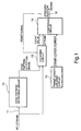
- Fig. 1 is a circuit diagram of a synchronization detecting circuit of a data processing apparatus according to an embodiment of the present invention.
- the detecting circuit comprises a sync pattern detecting circuit 12, a counting circuit 13, a comparing circuit 14, and a frame length holding circuit 15.
- the detecting circuit 12 inputs a bit stream of data via a data input terminal 11 and detects a predetermined data pattern in the bit stream.
- the bit stream contains a plurality of frames which each have the same length and which each contain a sync pattern corresponding to the predetermined data pattern.
- the detecting circuit 12 may be initially set with the predetermined data pattern. Then, as the incoming data in the bit stream is input, the circuit 12 compares the incoming data with the predetermined data pattern. When the incoming data matches the predetermined data pattern, the circuit 12 determines that the predetermined data pattern has been detected in the bit stream.
- the sync pattern detecting circuit 12 would determine that a sync pattern is contained in the bit stream when the incoming data equals "111111111111". When the detecting circuit 12 detects the predetermined data pattern in the bit stream, it outputs a sync pattern detection signal.
- the counting circuit 13 inputs the bit stream of data via the input terminal 11 and inputs the sync pattern detection signal from the detecting circuit 12. Upon receiving a first sync pattern detection signal from the detecting circuit 12, the counting circuit 13 begins counting the bits of data in the bit stream and outputs a corresponding count value. When a subsequent sync pattern detection signal is received from the detecting circuit 12, the counting circuit 13 stops counting the bits contained in the bit stream and outputs a strobe signal indicating that the second sync pattern detection signal has been detected. Afterwards, any additional sync pattern detection signals input by the counting circuit 13 alternatively cause the circuit 13 to begin counting the bits in the bit stream and to stop counting the bits in the bit stream.
- the counting circuit 13 comprises an RS flip-flop 300, first and second AND gates 302 and 304, and a counter 306.
- the flip-flop 300 inputs a sync pattern detection signal from the detecting circuit 12 via its set input and inputs a reset signal (described below) via its reset input.
- the first AND gate 302 inputs the sync pattern detection signal and an inverted output from the flip-flop 300, performs an AND operation on such signals, and outputs a start signal 402.
- the second AND gate 304 inputs the sync pattern detection signal and a non-inverted output from the flip-flop 300, performs an AND operation on such signals, and outputs a stop signal 406.
- the counter 306 inputs the bit stream from the input terminal 11, the start signal 402, and the stop signal 406, begins counting the number of bits of data in the bit stream after the start signal 402 is received, and outputs a corresponding count value.
- the counter 306 also stops counting the number of bits in the bit stream when the stop signal 406 is received.
- the reset signal is input to the counter 306 and resets the count value of the counter 306 to an initial value.
- the counting circuit 14 outputs the stop signal 406 as the strobe signal 408.
- the frame length holding circuit 15 comprises a memory (e.g. a read only memory (“ROM”), random access memory (“RAM”), etc) and stores a frame length number which corresponds to the number of bits contained in one frame of the bit stream. For example, if the bit stream is an MPEG audio bit stream, the bit rate is 192 kbps, and the sampling frequency is 48 kHz, the circuit 15 would store the number "4608" because such number corresponds to the number of bits in a frame of the MPEG audio bit stream.
- ROM read only memory
- RAM random access memory
- the comparing circuit 14 inputs the count value from the counting circuit 13 and inputs the frame length number stored in the frame length holding circuit 15. Then, the circuit 14 determines if the count value equals the frame length number. If the two numbers are equal, the comparing circuit 14 outputs a synchronization signal via an output terminal 16 to indicate that a sync pattern has been detected. On the other hand, if the count value does not equal the frame length number, the comparing circuit 14 outputs a reset signal via an output terminal 17. The reset signal is output to the counting circuit 13 and resets the count value of the counting circuit 13.
- Fig. 6 is a diagram of an example of an illustrative embodiment of the comparing circuit 14 shown in Fig. 1.
- the comparing circuit 14 comprises a data comparator 500 and an AND gate 502.
- the comparator 500 inputs the count value from the counter 306 and the frame length number from the holding circuit 15, compares the two numbers, and outputs a match signal which equals a logic "1" when the two numbers are equal.
- the AND gate 502 inputs the match signal from the comparator 500 and the strobe signal from the AND gate 304 and outputs a corresponding reset signal.
- Fig. 7 is a timing diagram which illustrates the operation of the counting circuit 13 and the comparing circuit 14.
- the flip-flop 300 Before a first sync pattern detection signal 400 is output from the detection circuit 12, the flip-flop 300 outputs a logic "0" as its non-inverted output, and thus, the inverted output equals a logic "1". Therefore, immediately when the signal 400 is output, the AND gate 302 inputs the detection signal 400 (i.e. a logic "1") and the inverted output (i.e. a logic "1") and outputs the start signal 402. As a result, the counter 306 begins counting the number of data bits in the bit stream and outputs the corresponding count value.
- the detection signal 400 is also input via the set input of the flip-flop 300 and causes the flip-flop to output a logic "1" as its non-inverted output. As a result, the inverted output equals a logic "0", and the AND gate 302 outputs a logic "0" as the start signal 402.
- the AND gate 304 inputs the signal 404 (i.e. a logic "1") and the non-inverted output of the flip-flop 300 (i.e. a logic "1") and outputs the stop signal 406.
- the counter 306 stops counting the number of data bits in the bit stream and outputs the corresponding count value.
- the strobe signal 408 is output when the stop signal 406 is generated.
- the AND gate 502 of the comparing circuit 14 outputs the match signal as the reset signal when the strobe signal is output.
- the match signal is output as the reset signal when the second sync pattern detection signal 404 is detected.
- the match signal is also output from the comparing circuit 14 as the synchronization signal.
- the comparing circuit 14 shown in Fig. 8 is similar to the circuit 14 shown in Fig. 6 except that the circuit further comprises a flip-flop 504.
- the flip-flop 504 inputs the output of the AND gate 502 and outputs such signal as the reset signal in synchronicity with a clock signal.
- Fig. 2 is a timing diagram of the various signals processed or generated by the synchronization detecting circuit. If the bit stream input via the input terminal 11 is an MPEG audio bit stream, the length of each frame in the bit stream equals 4608 bits, and the sync pattern in each frame equals the data pattern "111111111111".
- the sync pattern detecting circuit 12 When the sync pattern detecting circuit 12 detects the first sync pattern 21 in the bit stream, it outputs a first sync pattern detection signal 30. As a result, the counting circuit 13 begins counting the bits in the bit stream and incrementing its count value. After the 3000th bit in the bit stream has been counted, a data pattern 22 in the ancillary data portion of the first frame of the bit stream equals "111111111111". As a result, the sync pattern detecting circuit 12 outputs a second sync pattern detection signal 31, and the counting circuit 13 stops counting the bits in the bit stream, outputs the count value "3000" to the comparing circuit 14, and outputs the strobe signal to the comparing circuit. Upon comparing the count value "3000" with the frame length number "4608", the comparing circuit 14 determines that such numbers are not equal and outputs the reset signal 40. As a result, the count value in the counting circuit 13 is reset to an initial value.
- the count value remains at the initial value until the sync pattern 23 of the second frame is detected by the detecting circuit 12.
- the circuit 12 outputs a third sync pattern detection signal 32, and the counting circuit 13 begins incrementing the internal count value by counting the bits in the bit stream. This process continues until the detecting circuit 12 sequentially detects two actual sync patterns in the bit stream.
- a sync pattern detection signal 33 is output to the counting circuit 13, and the circuit 13 begins counting the bits in the bit stream. Then, when the next sync pattern 25 is detected by the detecting circuit 12, a sync pattern detection signal 34 is output to the counting circuit 13. As a result, the circuit 13 stops counting the bits in the bit stream and outputs the count value "4608" and the strobe signal. Since the count value "4608" equals the frame length number "4608" stored in the frame length holding circuit 15, the comparing circuit 14 outputs the synchronization signal 50.
- the synchronization detecting circuit of the present embodiment since the synchronization detecting circuit of the present embodiment only generates the synchronization signal when two actual sync patterns are sequentially detected, the circuit cannot erroneously detect ancillary data as a sync pattern. As a result, the synchronization detecting circuit enables a reproducing apparatus to consistently reproduce audio data from a bit stream without generating noise.
- the present invention is not limited to the specific embodiments described above.
- the invention is not limited to detecting sync patterns in an MPEG audio bit stream.
- the present invention can detect any predetermined data pattern in a bit stream which has frames that are a constant length and in which the data pattern is transmitted in the same location of each of the data frames.
- the detecting apparatus is constructed via hardware.
- the apparatus may be implemented via software or a combination of hardware and software.
- MPEG data is typically reproduced by using hardware circuitry known as an "MPEG board".
- the MPEG data may be reproduced via a computer or processor by using an application program (i.e. a "soft PEG").
- the application program instructs the processor to simulate the data detection operation described above in conjunction with the synchronization detecting circuit and may be stored as in an information storage medium such as a ROM, a RAM, a hard disk drive (“HDD”), a CD-ROM, or a floppy disk (“FD").
- the program may be stored in the information storage medium which supplies the synchronization detecting software to the processor.
- the program may instruct the processor to input a bit stream and detect a particular data pattern in the bit stream.
- the program may instruct the processor to begin generating a count value by counting the number of bits in the bit stream when the data pattern is first detected in the bit stream and to stop counting the bits in the bit stream when the data pattern is subsequently detected in the bit stream.
- the program may instruct the processor to compare the count value with a predetermined value. If the count value equals the predetermined value, the program may instruct the processor to output a synchronization signal. On the other hand, if the values are not equal, the program may instruct the processor to reset the count value to an initial value. After the count value is reset, the program may instruct the processor to begin counting the number of bits in the bit stream when a subsequent data pattern is detected.
- the present invention is capable of accurately synchronizing a data processing apparatus with data in a bit stream by detecting two sequential sync patterns in a bit stream.
- Three situations may occur in which ancillary data could potentially be mistakenly detected as a sync pattern.
- an actual sync pattern may be initially detected in the bit stream, and then, ancillary data in an ancillary data portion of a frame may be mistakenly detected as a sync pattern.
- the ancillary data may be initially and erroneously detected as a sync pattern, and then, an actual sync pattern may be detected.
- a first set of ancillary data contained in the ancillary data portion may be initially and erroneously detected as a sync pattern, and then, a second set of ancillary data contained in the same ancillary data portion may be detected as a sync pattern.
- the count value output to the comparing circuit 14 (or processed via software) will not equal the number of bits in a frame of the bit stream.
- the count value is reset, the ancillary data is not detected as a sync pattern, and a synchronization signal is not generated.
- the actual sync patterns within the bit stream can be more quickly detected to synchronize the data processing apparatus with the data in the bit stream.
Landscapes
- Engineering & Computer Science (AREA)
- Computer Networks & Wireless Communication (AREA)
- Signal Processing (AREA)
- Synchronisation In Digital Transmission Systems (AREA)
- Signal Processing For Digital Recording And Reproducing (AREA)
Applications Claiming Priority (3)
| Application Number | Priority Date | Filing Date | Title |
|---|---|---|---|
| JP14673697 | 1997-06-04 | ||
| JP14673697 | 1997-06-04 | ||
| JP146736/97 | 1997-06-04 |
Publications (2)
| Publication Number | Publication Date |
|---|---|
| EP0883262A2 true EP0883262A2 (fr) | 1998-12-09 |
| EP0883262A3 EP0883262A3 (fr) | 2003-12-17 |
Family
ID=15414438
Family Applications (1)
| Application Number | Title | Priority Date | Filing Date |
|---|---|---|---|
| EP98110164A Withdrawn EP0883262A3 (fr) | 1997-06-04 | 1998-06-04 | Circuit de détection de signal de synchronisation, procédé et support de stockage d'information |
Country Status (2)
| Country | Link |
|---|---|
| US (1) | US6272194B1 (fr) |
| EP (1) | EP0883262A3 (fr) |
Cited By (1)
| Publication number | Priority date | Publication date | Assignee | Title |
|---|---|---|---|---|
| KR100332417B1 (ko) * | 1999-11-23 | 2002-04-13 | 서평원 | 에스티엠-16 프레임 패턴 검출 장치 |
Families Citing this family (17)
| Publication number | Priority date | Publication date | Assignee | Title |
|---|---|---|---|---|
| US6501810B1 (en) * | 1998-10-13 | 2002-12-31 | Agere Systems Inc. | Fast frame synchronization |
| EP1067721A1 (fr) * | 1999-07-06 | 2001-01-10 | Sony International (Europe) GmbH | Détecteur de synchronisation de paquets |
| EP1119122A3 (fr) * | 2000-01-20 | 2005-01-19 | Matsushita Electric Industrial Co., Ltd. | Méthode de radiodiffusion numérique, émetteur de radiodiffusion pour l'émission de signaux de radiodiffusion numérique ainsi que récepteur pour la réception de ces signaux de radiodiffusion numérique |
| US7406104B2 (en) * | 2000-08-25 | 2008-07-29 | Lin Yang | Terrestrial digital multimedia/television broadcasting system |
| US6907045B1 (en) * | 2000-11-17 | 2005-06-14 | Nortel Networks Limited | Method and apparatus for data-path conversion comprising PCM bit robbing signalling |
| JP4342287B2 (ja) * | 2003-02-06 | 2009-10-14 | 三洋電機株式会社 | デコード装置 |
| US7212364B1 (en) * | 2004-01-31 | 2007-05-01 | Western Digital Technologies, Inc. | Servo writing a disk drive by synchronizing a servo write clock in response to a sync mark reliability metric |
| US7440210B1 (en) | 2004-06-23 | 2008-10-21 | Western Digital Technologies, Inc. | Servo writing a disk drive by writing multi-bit sync marks in spiral tracks for improved servo writing |
| US7330327B1 (en) | 2004-06-23 | 2008-02-12 | Western Digital Technologies, Inc. | Servo writing a disk drive by writing discontinuous spiral tracks to prevent overheating |
| US7333280B1 (en) | 2004-08-03 | 2008-02-19 | Western Digital Technologies, Inc. | Servo writing a disk drive by synchronizing a servo write clock to a reference pattern on the disk and compensating for repeatable phase error |
| US8121228B2 (en) * | 2005-11-04 | 2012-02-21 | Freescale Semiconductor, Inc. | Detecting a data frame |
| EP1826932B1 (fr) * | 2006-02-22 | 2011-07-06 | Media Evolution Technologies Inc. | Méthode et appareil pour la génération de signatures numériques de signaux audiophoniques |
| US7391583B1 (en) | 2006-07-27 | 2008-06-24 | Western Digital Technologies, Inc. | Fault tolerant sync mark detection while servo writing a disk drive from spiral tracks |
| US8059754B2 (en) * | 2006-07-28 | 2011-11-15 | Xg Technology, Inc. | System and method for fast signal acquisition in a wireless digital receiver for wideband signals |
| KR100884003B1 (ko) * | 2007-01-26 | 2009-02-17 | 삼성전자주식회사 | 기입 오류 방지 방법, 및 그에 따른 하드 디스크 드라이브 장치 |
| JP5036353B2 (ja) * | 2007-03-13 | 2012-09-26 | オンセミコンダクター・トレーディング・リミテッド | データ再生装置及びデータ再生方法 |
| US7859782B1 (en) | 2008-05-18 | 2010-12-28 | Western Digital Technologies, Inc. | Selecting highest reliability sync mark in a sync mark window of a spiral servo track crossing |
Family Cites Families (12)
| Publication number | Priority date | Publication date | Assignee | Title |
|---|---|---|---|---|
| US4580129A (en) * | 1983-11-14 | 1986-04-01 | Northern Telecom Limited | Variable word length decoder |
| JP2603215B2 (ja) * | 1985-07-04 | 1997-04-23 | キヤノン株式会社 | 画像認識方法及び装置 |
| JPH01200840A (ja) * | 1988-02-05 | 1989-08-14 | Nippon Telegr & Teleph Corp <Ntt> | セル同期方式 |
| JPH03102939A (ja) * | 1989-09-14 | 1991-04-30 | Toshiba Corp | セル同期方式 |
| DE69027531D1 (de) * | 1990-09-28 | 1996-07-25 | Ibm | Datenübertragungseinheit (DCE) mit einer durch ein Verarbeitungsmittel gesteuerten Taktgeberanordnung |
| JPH04342327A (ja) | 1991-05-20 | 1992-11-27 | Nec Corp | 同期検出回路 |
| JPH0832571A (ja) | 1994-07-12 | 1996-02-02 | Nec Eng Ltd | フレーム信号検出方式 |
| JP3412927B2 (ja) | 1994-09-30 | 2003-06-03 | 株式会社東芝 | フレーム同期回路 |
| JPH08125649A (ja) | 1994-10-19 | 1996-05-17 | Fujitsu Ltd | フレーム同期検出方式 |
| JPH08149118A (ja) | 1994-11-25 | 1996-06-07 | Matsushita Electric Ind Co Ltd | 同期信号検出装置 |
| JP2817660B2 (ja) * | 1995-03-30 | 1998-10-30 | 日本電気株式会社 | 同期回路 |
| JP2861932B2 (ja) * | 1996-05-22 | 1999-02-24 | 日本電気株式会社 | バーストフレーム位相同期回路 |
-
1998
- 1998-06-04 US US09/090,146 patent/US6272194B1/en not_active Expired - Fee Related
- 1998-06-04 EP EP98110164A patent/EP0883262A3/fr not_active Withdrawn
Cited By (1)
| Publication number | Priority date | Publication date | Assignee | Title |
|---|---|---|---|---|
| KR100332417B1 (ko) * | 1999-11-23 | 2002-04-13 | 서평원 | 에스티엠-16 프레임 패턴 검출 장치 |
Also Published As
| Publication number | Publication date |
|---|---|
| EP0883262A3 (fr) | 2003-12-17 |
| US6272194B1 (en) | 2001-08-07 |
Similar Documents
| Publication | Publication Date | Title |
|---|---|---|
| US6272194B1 (en) | Synchronous signal detecting circuit, method, and information storage medium | |
| US4412306A (en) | System for minimizing space requirements for storage and transmission of digital signals | |
| US4596981A (en) | Synchronizing signal detecting circuit in a digital signal transmitting system | |
| US4280192A (en) | Minimum space digital storage of analog information | |
| EP0166023A2 (fr) | Méthode et système pour la compression et l'expansion de données | |
| GB2038593A (en) | Apparatus for extracting a synchronizing signal | |
| EP0735709B1 (fr) | Circuit de synchronisation pour un système de compression et de décompression d'un signal de son numérique | |
| CN101266820B (zh) | 数据再生装置及数据再生方法 | |
| US6683825B2 (en) | Optical disk drive unit | |
| US5696867A (en) | Apparatus in digital video tape recorder for detecting a sync signal in digital data | |
| EP0599290B1 (fr) | Appareil d'extraction d'un signal de synchronisation | |
| JPS6016027B2 (ja) | タイムコ−ド読取装置 | |
| JPS6016028B2 (ja) | タイムコ−ド読取装置 | |
| US7542390B2 (en) | Method for sampling optical disc data and apparatus thereof | |
| US6209117B1 (en) | Method for canceling abnormal synchronization signal | |
| JPH117708A (ja) | 同期検出回路 | |
| JPH1155237A (ja) | データ処理装置および方法、情報記憶媒体 | |
| US5936922A (en) | Method and apparatus for sampling a synchronous pattern from data including an error using a random synchronous signal | |
| JPH06132923A (ja) | デジタルデータ受信回路 | |
| US5995307A (en) | Method of forcibly judging a sector synchronous signal for a disk reproducing apparatus | |
| KR19990003394A (ko) | 싱크패턴 검출기 | |
| JPH0264965A (ja) | データ識別装置及びデータフォーマット | |
| JP3406113B2 (ja) | ブロック化データ転送同期ずれ検出装置 | |
| JP2553072B2 (ja) | 同期回路 | |
| CA1168360A (fr) | Stockage numerique de donnees analogiques dans un espace minimum |
Legal Events
| Date | Code | Title | Description |
|---|---|---|---|
| PUAI | Public reference made under article 153(3) epc to a published international application that has entered the european phase |
Free format text: ORIGINAL CODE: 0009012 |
|
| AK | Designated contracting states |
Kind code of ref document: A2 Designated state(s): AT BE CH CY DE DK ES FI FR GB GR IE IT LI LU MC NL PT SE |
|
| AX | Request for extension of the european patent |
Free format text: AL;LT;LV;MK;RO;SI |
|
| RAP1 | Party data changed (applicant data changed or rights of an application transferred) |
Owner name: NEC ELECTRONICS CORPORATION |
|
| PUAL | Search report despatched |
Free format text: ORIGINAL CODE: 0009013 |
|
| AK | Designated contracting states |
Kind code of ref document: A3 Designated state(s): AT BE CH CY DE DK ES FI FR GB GR IE IT LI LU MC NL PT SE |
|
| AX | Request for extension of the european patent |
Extension state: AL LT LV MK RO SI |
|
| RIC1 | Information provided on ipc code assigned before grant |
Ipc: 7H 04L 7/08 B Ipc: 7H 04L 7/04 A |
|
| 17P | Request for examination filed |
Effective date: 20031106 |
|
| 17Q | First examination report despatched |
Effective date: 20040223 |
|
| AKX | Designation fees paid |
Designated state(s): DE FR GB |
|
| STAA | Information on the status of an ep patent application or granted ep patent |
Free format text: STATUS: THE APPLICATION IS DEEMED TO BE WITHDRAWN |
|
| 18D | Application deemed to be withdrawn |
Effective date: 20040706 |