EP0884847A2 - Circuit de sortie à faible amplitude de signal - Google Patents
Circuit de sortie à faible amplitude de signal Download PDFInfo
- Publication number
- EP0884847A2 EP0884847A2 EP98110832A EP98110832A EP0884847A2 EP 0884847 A2 EP0884847 A2 EP 0884847A2 EP 98110832 A EP98110832 A EP 98110832A EP 98110832 A EP98110832 A EP 98110832A EP 0884847 A2 EP0884847 A2 EP 0884847A2
- Authority
- EP
- European Patent Office
- Prior art keywords
- output
- level
- circuit
- transistor
- voltage
- Prior art date
- Legal status (The legal status is an assumption and is not a legal conclusion. Google has not performed a legal analysis and makes no representation as to the accuracy of the status listed.)
- Granted
Links
- 230000008859 change Effects 0.000 claims description 32
- 238000000034 method Methods 0.000 abstract description 5
- 238000004519 manufacturing process Methods 0.000 abstract description 4
- 230000008569 process Effects 0.000 abstract description 4
- 230000005540 biological transmission Effects 0.000 description 31
- 238000010586 diagram Methods 0.000 description 12
- 230000008901 benefit Effects 0.000 description 9
- 230000014509 gene expression Effects 0.000 description 8
- 230000007423 decrease Effects 0.000 description 6
- 239000000470 constituent Substances 0.000 description 5
- 230000009467 reduction Effects 0.000 description 5
- 230000008054 signal transmission Effects 0.000 description 5
- 238000006243 chemical reaction Methods 0.000 description 4
- 238000004088 simulation Methods 0.000 description 2
- BNPSSFBOAGDEEL-UHFFFAOYSA-N albuterol sulfate Chemical compound OS(O)(=O)=O.CC(C)(C)NCC(O)C1=CC=C(O)C(CO)=C1.CC(C)(C)NCC(O)C1=CC=C(O)C(CO)=C1 BNPSSFBOAGDEEL-UHFFFAOYSA-N 0.000 description 1
- 230000004075 alteration Effects 0.000 description 1
- 230000005674 electromagnetic induction Effects 0.000 description 1
- 230000004048 modification Effects 0.000 description 1
- 238000012986 modification Methods 0.000 description 1
- 102220023133 rs387907398 Human genes 0.000 description 1
- 102220263036 rs745885744 Human genes 0.000 description 1
- 230000011664 signaling Effects 0.000 description 1
Images


Classifications
-
- H—ELECTRICITY
- H03—ELECTRONIC CIRCUITRY
- H03K—PULSE TECHNIQUE
- H03K19/00—Logic circuits, i.e. having at least two inputs acting on one output; Inverting circuits
- H03K19/0175—Coupling arrangements; Interface arrangements
- H03K19/017509—Interface arrangements
- H03K19/017518—Interface arrangements using a combination of bipolar and field effect transistors [BIFET]
-
- H—ELECTRICITY
- H03—ELECTRONIC CIRCUITRY
- H03K—PULSE TECHNIQUE
- H03K19/00—Logic circuits, i.e. having at least two inputs acting on one output; Inverting circuits
- H03K19/003—Modifications for increasing the reliability for protection
- H03K19/00369—Modifications for compensating variations of temperature, supply voltage or other physical parameters
Definitions
- the present invention relates to a small amplitude signal output circuit and, more particularly, to a small amplitude signal output circuit transmitting logic signals between integrated circuits by way of a transmission line.
- Some output circuits are used as signal transmission means for transmitting signals between two or more integrated circuits via transmission paths such as bus lines.
- the logic signal assumes either H-level or L-level of logical value. Accordingly, there essentially exist, in an output circuit of an integrated circuit, an input terminal for receiving internal logic signals from the internal circuit of the integrated circuit, and an output terminal for delivering the internal logic signals to another integrated circuit.
- the signal amplitude has been reduced for transmission in recent years.
- the signal amplitude was substantially equal to the power source potential such as about 5V or about 3V.
- the recent transmission signal having a small amplitude such as used in a low voltage differential signaling (LVDS) interface
- the signal amplitude is as low as about 0.3V. The reason for reduction of the signal amplitude is that the reduction achieves great advantages in higher transmission speed, lower power dissipation, and smaller noise during signal transmission.
- integrated circuits for achieving a higher speed and/or lower power dissipation as the primary objects thereof have an output circuit capable of outputting lower amplitude signals.
- output circuit capable of outputting lower amplitude signals.
- the output circuit comprises: a PMOS transistor M11 having a source connected to source line VDD of positive potential, a drain connected to output terminal OUT1 which outputs a low amplitude signal and a gate connected to input terminal IN1; an NMOS transistor M12 having a drain connected to the drain of transistor M11, a gate connected to the gate of transistor M11, and a source connected to source line VSS of ground potential; and a terminal resistor RTT1, having a first terminal connected to output terminal OUT1 and a second terminal connected to a terminal power source VTT.
- PECL interface Pseudo Emitter Coupled Logic interface
- source line VDD positive potential is supplied from outside the integrated circuit to source line VDD and source line VSS is grounded.
- source line VDD is grounded, and a negative potential is supplied to source line VSS.
- terminal resistor RTT1 and terminal power source potential VTT are generally specified in a standard wherein the former is about 50 ⁇ , and the latter is obtained by subtracting about 2V from the power source potential VDD.
- VOL VTT- ⁇ (VTT-VSS) ⁇ RTT ⁇ /(RTT+RONN) wherein VTT, VSS, RTT and RONN represent potential of power source VTT, potential of source line VSS, resistance of resistor RTT1 and ON-resistance of NMOS transistor M12, respectively.
- the conventional output circuit has a feature that it enables to obtain a desired small signal amplitude by selecting ON-resistances RONP and RONN, which are adjusted based on the size of the transistor elements in the integrated circuit, depending on the power source potentials VDD, VSS, VTT, and terminal resistor RTT which are specified in advance.
- the first conventional output circuit Since the first conventional output circuit has a single output terminal for transmission of a single signal, it is generally called a single phase transmission system.
- differential transmission system As another transmission system having a low signal amplitude interface, so-called differential transmission system is also used which outputs a pair of transmission signals from respective output terminals.
- the pair of transmission signals in the differential transmission system have a feature that the phase of the pair of signals are reversed from each other and have equal potentials of H-level and L-level.
- the reversed phase scheme in the differential transmission system provides a twice dynamic range compared to the single phase transmission system.
- there is an advantage that the influence by noise in the power source potential and interference by electromagnetic induction are reduced.
- the differential transmission system is used for a high-speed and high-reliability transmission.
- Fig. 2 shows a second conventional output circuit for LVDS interface as a typical differential transmission system, wherein similar constituent elements are designated by reference symbols similar to those used in Fig. 1.
- the output circuit comprises: a first output section 11 having transistors M11 and M12, terminal transistor RTT1, input terminal IN1 and output terminal OUT1, which are common to the first conventional output circuit; and a second output section 12 having constituent elements similar to those in the first output section 11.
- the second output section 12 comprises PMOS transistor M21 having a source connected to positive potential source line VDD, a drain connected to output terminal OUT2 and a gate connected to input terminal IN2, NMOS transistor M22 having a drain connected to the drain of transistor M21, a gate connected to the gate of transistor M21, and a source connected to grounded potential source line VSS, terminal resistor RTT2 having a first terminal connected to output OUT2 ad a second terminal connected to terminal source VTT.
- terminal resistors RTT1 and RTT2 are generally specified in a standard, wherein RTT1 and RTT2 are set at about 45 to 65 ⁇ and VTT is set at about 1.1V to 1.4V.
- H-level potential which is close to potential VDD of source line VDD is supplied to input terminal IN1
- L-level potential which is close to potential VSS of source line VSS is supplied to input terminal IN2
- transistors M12 and M21 are ON
- transistors M11 and M22 are OFF.
- a current path is formed from source line VDD to terminal source VTT via transistor M21 and terminal resistor RTT2
- another current path is formed from terminal source VTT to source line VSS via terminal resistor RTT1 and transistor M12.
- output terminal OUT1 supplies an L-level signal
- output terminal OUT2 supplies an H-level signal.
- H-level signal potential VOH and L-level signal potential VOH are given by the expressions (1) and (2) as mentioned before.
- H-level signal VOH and L-level signal VOL are equal to the above-mentioned numerical values (3), (4) and (5).
- the first factor is the influence by variations in the fabrication process of the MOS transistors.
- the fabrication process involves variation factors which affect shape variations in the transistor elements which constitute the output circuit. For example, variations in ON-resistance of the MOS transistor range generally about ⁇ 10% to ⁇ 20% depending on the shape of the transistor.
- the second factor is the influence by the ambient temperatures at which the electronic device equipped with the integrated circuit is used under various environments.
- the ON-resistance of the MOS transistor changes, especially with the change of the ambient temperature: for example, the variations generally range about ⁇ 8% to ⁇ 16% with respect to a temperature rage of 100°C.
- the third factor is the influence by the variations in the power source potential.
- the power source potential supplied from outside the integrated circuit changes due to the potential loss on the source line in addition to the potential change of the external power source itself.
- the ON-resistance of the MOS transistor changes with the change of the input voltage: for example, the variations generally range about ⁇ 10% to ⁇ 15% with respect to a power source potential change of ⁇ 10%.
- the variations in the ON-resistance of the MOS transistor generally range about ⁇ 28% to 51% when taking into account all the three factors mentioned above.
- the variations in the signal amplitude VOH-VOL are 1.7 times greater than the case in which the signal amplitude is calculated from the ON-resistance of the MOS transistor when the three factors are not taken into account namely 0.6V, as shown in expression (3).
- Variations in the output signal amplitude especially in the case of variations in the higher direction, reduce and cancel the advantages of the small amplitude transmission described before.
- the first and the second conventional output circuits have a problem of large variations in the signal amplitude to be solved, which cause reduction in transmission speed, increase in power dissipation and increase in the noise during signal transmission.
- the present invention provides a small amplitude signal output circuit comprising:
- variations in the signal amplitude of an output signal supplied from the output circuit can be suppressed by the feedback function of the first level sense circuit and the level control circuit, thereby suppressing reduction in transmission speed, increase in power dissipation and increase in the noise during signal transmission.
- the output circuit comprises an output section 11 having PMOS transistors M11 and M12, a terminal resistor RTT1, an input terminal IN1 and an output terminal OUT1, which are similar to those in the first conventional output circuit.
- the output circuit comprises a level sense circuit 13 for detecting variations in the voltage level of output terminal OUT1, and a level control circuit 15 for controlling output voltage level by responding to the variations in the voltage level detected by level sense circuit 13.
- Level sense circuit 13 comprises an NMOS transistor M31 having a gate connected to output terminal OUT1 and an NMOS transistor M32 having a gate and a drain connected together, for a diode connection, to the drain of transistor M31 and a source connected to power source line VSS.
- Level control circuit 15 comprises: an NPN bipolar transistor M51 having a collector connected to source line VDD, a base connected to the drain of transistor M31 in level sense circuit 13 and an emitter connected to the source of transistor M11 in output section 11; and a resistor R51 having a first terminal connected to the base of transistor M51 and a second terminal connected to source line VDD.
- the output circuit suppresses the variations in H-level voltage VOH of the output signal thereof. Specifically, when an L-level signal having a potential close to the potential of source line VSS is supplied to input terminal IN, transistor M11 and M12 of output circuit 11 are ON and OFF, respectively, transistor M51 of level control circuit 15 is ON. Thus, a current path is formed from source line VDD to terminal source line VTT via transistor M51, transistor M11 and terminal resistor RTT1.
- transistors M31 and M32 of level sense circuit 13 increase ON-current flowing from the drain of transistor M31 to source line VSS via transistor M32.
- the continuous current I31 generates a voltage drop across resistor R51 of level control circuit 15 which functions as a current/voltage converter.
- source potential of transistor M11 falls to raise the ON-resistance RONP11 of transistor M11, thereby canceling the initial decrease of the ON-resistance of transistor M11 to maintain the H-level voltage VOH at a design value, as understood from equation (2).
- the output circuit of the present embodiment is similar to the first embodiment except that the output circuit comprises: a level sense circuit 13A, instead of level sense circuit 13 of Fig. 3, including PMOS transistor M33 having a gate connected to output terminal OUT1, a PMOS transistor M34 having a drain and a gate connected together, for a diode connection, to the drain of transistor M33 and a source connected to power source VDD; and a level control circuit 15A, instead of level control circuit 15 of Fig.
- PNP bipolar transistor M52 having a collector, a base and an emitter which are connected to power source VSS, the drain of transistor M33 of level sense circuit 13A and the source of transistor M11 of output portion 11, respectively, and a resistor R52 having a first terminal connected the base of transistor M52 and a second terminal connected to source line VSS.
- the output circuit of the present embodiment suppresses the variations in L-level VOL of the output signal thereof. Specifically, when an H-level signal having a potential close to source line VDD is supplied to input terminal IN, transistors M11 and M12 of output circuit 11 are OFF and ON, respectively, and transistor M52 of level control circuit 15A is ON. Thus, a current path is formed from source line VTT to source line VSS via transistor M52, transistor M12 and terminal resistor RTT1.
- transistors M33 and M34 of the level sense circuit 13A increase ON-current flowing from source line VDD through the drain of transistor M33 toward the drain of transistor M34 of level sense circuit 13A.
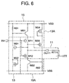
- the output circuit of the present invention comprises the constituent elements of both the first embodiment and the second embodiment.
- the output circuit of the present embodiment comprises an output section 11, having transistors M11 and M12, for responding to an input supplied through an input terminal IN1 to deliver an output signal from an output terminal OUT1, a level sense circuit 13, having transistors M31 and M32, for sensing the output voltage at OUT1, a level sense circuit 13A, having transistors M33 and M34, for sensing the output voltage at OUT1, a level control circuit 15, having transistors M51 and resistor R51, for responding to the current of level sense circuit 13, and a level control circuit 15A, having transistors M52 and resistor R52, for responding to the current of level sense circuit 13A.
- the output circuit of the present embodiment suppresses the variations in both H-level voltage VOH and L-level voltage VOL of the output signal. Specifically, when L-level signal having a potential close to source line VSS is supplied to input terminal IN, an operation similar to the first embodiment is effected to suppress the change of H-level VOH of the output signal by the function of level sense circuit 13 and level control circuit 15. In addition, when H-level signal having a potential close to source line VDD is supplied to input terminal IN, an operation similar to the second embodiment is effected to suppress the change of L-level VOL of the output signal by the function of level sense circuit 13A and level control circuit 15A.
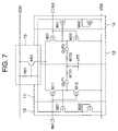
- the output circuit of the present embodiment comprises, in addition to the constituent elements (output section 11, level sense circuit 13 and level control circuit 15) of the first embodiment, an output section 12 having a PMOS transistor M21 having a source connected to source line VDD of positive potential, a drain connected to output terminal OUT2, and a gate connected to input terminal IN2, an NMOS transistor M22 having a drain connected to the drain of transistor M21, a gate connected to the gate of transistor M21, and a source connected to source line VSS of ground potential, and a terminal resistor RTT2 having a first terminal connected to output terminal OUT2 and a second terminal connected to terminal source VTT; and a level sense circuit 14 having an NMOS transistor M41 having a drain connected to the emitter of transistor M51 of level control circuit 15 and a gate connected to output terminal OUT1, and an NM
- the output circuit of the present embodiment implemented as a differential transmission system, comprises a pair of input terminals IN1 and IN2, and a pair of output terminals OUT1 and OUT2.
- output section 11 connected to a pair of input terminal IN1 and output terminal OUT1, level sense circuit 13 and level control circuit 15 are similar to those in the first embodiment implemented as a single phase transmission system.
- Output section 12 connected to a pair of input terminal IN2 and output terminal OUT2, and level sense circuit 14 are also similar to those shown in Fig. 3.
- the operation and the advantages in the present embodiment are similar to those in the first embodiment as to output sections 11 and 12, level sense circuits 13 and 14 and level control circuit 15. It is to be noted that a single level control circuit 15 is provided herein in view of simplification of the output circuit. It is possible, however, to provide a pair of level control circuits in the present embodiment, although operation and advantages improve little from the single level control circuit 15.
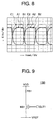
- Fig. 8 is a signal timing chart obtained by a simulation for the present embodiment, showing waveforms "A1" and “A2" of respective output terminals OUT1 and OUT2 in the present embodiment when the three factors in transistors M11 and M21 are taken into account in comparison with ideal waveforms "B1” and “B2" when the three factors are not taken into account, and waveforms "C1” and “C2" of the second conventional output circuit when the three factors are taken into account.
- H-level VOH of the output signal rises about 43% due to the influence by the three factors in waveforms "C1" and “C2" of the second conventional output circuit, whereas, the variation of H-level VOH of the output signal is suppressed by 7% in waveforms "A1" and "A2" of the present embodiment.
- Fig. 4 shown for the single phase transmission system of the first embodiment.
- the output circuit of the present invention may be applied to both the single phase transmission system and the differential transmission system.
- the configuration of the first embodiment is applied to the differential transmission system. It is also possible to apply the configurations of the second and third embodiment to the differential transmission system.
- the sense transistor of level sense circuit is implemented by NMOS/PMOS transistor. It is also possible to implement the sense transistor of level sense circuit by NPN/PNP bipolar transistor.
- the current/voltage converter of the level control circuit is implemented by a resistor; however, it is also possible to implement the resistor element by a PMOS/NMOS transistor or PNP/NPN bipolar transistor. It is also possible that the level control transistor of the level control circuit is implemented by a NMOS/PMOS transistor instead of the NPN/PNP bipolar transistor.
- level sense circuit 13B comprises a transistor M31 having a source supplied with a reference voltage VREF instead of providing transistor M32 having a diode connection.
- Transistor M31 is similar to that shown in Fig. 3.
- level sense circuit 13 of Fig. 3 converts variations in H-level VOH of the output signal into continuous current change I33 as shown in expression (10).
- level sense circuit 13B of Fig. 9 the gate-source potential VGS of transistor M31 is controlled at a desired value by controlling the reference voltage VREF. This configuration provides an additional advantage that a more accurate output voltage can be sensed.
Landscapes
- Engineering & Computer Science (AREA)
- Computer Hardware Design (AREA)
- Physics & Mathematics (AREA)
- Computing Systems (AREA)
- General Engineering & Computer Science (AREA)
- Mathematical Physics (AREA)
- Logic Circuits (AREA)
Applications Claiming Priority (3)
| Application Number | Priority Date | Filing Date | Title |
|---|---|---|---|
| JP15651997 | 1997-06-13 | ||
| JP9156519A JP3000962B2 (ja) | 1997-06-13 | 1997-06-13 | 出力回路 |
| JP156519/97 | 1997-06-13 |
Publications (3)
| Publication Number | Publication Date |
|---|---|
| EP0884847A2 true EP0884847A2 (fr) | 1998-12-16 |
| EP0884847A3 EP0884847A3 (fr) | 1999-04-07 |
| EP0884847B1 EP0884847B1 (fr) | 2004-12-01 |
Family
ID=15629568
Family Applications (1)
| Application Number | Title | Priority Date | Filing Date |
|---|---|---|---|
| EP98110832A Expired - Lifetime EP0884847B1 (fr) | 1997-06-13 | 1998-06-12 | Circuit de sortie à faible amplitude de signal |
Country Status (5)
| Country | Link |
|---|---|
| US (1) | US6052018A (fr) |
| EP (1) | EP0884847B1 (fr) |
| JP (1) | JP3000962B2 (fr) |
| CN (1) | CN1168211C (fr) |
| DE (1) | DE69827877T2 (fr) |
Families Citing this family (4)
| Publication number | Priority date | Publication date | Assignee | Title |
|---|---|---|---|---|
| JP3285088B2 (ja) * | 1999-09-08 | 2002-05-27 | 日本電気株式会社 | Emiノイズ除去機構を備える波形出力装置 |
| US6839792B2 (en) * | 2000-12-15 | 2005-01-04 | Innovative Concepts, Inc. | Data modem |
| US20090128119A1 (en) * | 2007-11-16 | 2009-05-21 | Fujitsu Microelectronics Limited | Differential output circuit |
| CN102088284B (zh) * | 2010-12-24 | 2013-01-02 | 厦门优迅高速芯片有限公司 | 一种pecl电平接口电路 |
Family Cites Families (6)
| Publication number | Priority date | Publication date | Assignee | Title |
|---|---|---|---|---|
| JPH01295508A (ja) * | 1988-05-23 | 1989-11-29 | Mitsubishi Electric Corp | 出力回路 |
| JPH02177724A (ja) * | 1988-12-28 | 1990-07-10 | Sumitomo Electric Ind Ltd | 出力バッファ回路 |
| DE4007212A1 (de) * | 1990-03-07 | 1991-09-12 | Siemens Ag | Integrierbare transistorschaltung zur abgabe logischer pegel |
| US5334882A (en) * | 1992-12-14 | 1994-08-02 | National Semiconductor | Driver for backplane transceiver logic bus |
| US5378943A (en) * | 1993-04-20 | 1995-01-03 | International Business Machines Corporation | Low power interface circuit |
| US5440243A (en) * | 1993-09-21 | 1995-08-08 | Apple Computer, Inc. | Apparatus and method for allowing a dynamic logic gate to operation statically using subthreshold conduction precharging |
-
1997
- 1997-06-13 JP JP9156519A patent/JP3000962B2/ja not_active Expired - Fee Related
-
1998
- 1998-06-12 DE DE69827877T patent/DE69827877T2/de not_active Expired - Lifetime
- 1998-06-12 EP EP98110832A patent/EP0884847B1/fr not_active Expired - Lifetime
- 1998-06-12 US US09/096,169 patent/US6052018A/en not_active Expired - Lifetime
- 1998-06-13 CN CNB98102985XA patent/CN1168211C/zh not_active Expired - Fee Related
Also Published As
| Publication number | Publication date |
|---|---|
| EP0884847A3 (fr) | 1999-04-07 |
| EP0884847B1 (fr) | 2004-12-01 |
| JPH114158A (ja) | 1999-01-06 |
| DE69827877T2 (de) | 2005-04-21 |
| JP3000962B2 (ja) | 2000-01-17 |
| DE69827877D1 (de) | 2005-01-05 |
| US6052018A (en) | 2000-04-18 |
| CN1208995A (zh) | 1999-02-24 |
| CN1168211C (zh) | 2004-09-22 |
Similar Documents
| Publication | Publication Date | Title |
|---|---|---|
| JP5065424B2 (ja) | リンギング抑制回路 | |
| US5999041A (en) | Load actuation circuit | |
| EP0621694B1 (fr) | Circuit d'interface à faible consommation | |
| US7501853B2 (en) | Data processing circuit | |
| US5059890A (en) | Constant current source circuit | |
| KR910006696B1 (ko) | 출력 인터페이스회로 | |
| US7319575B2 (en) | Semiconductor device | |
| JPH02162812A (ja) | 相補形カレント・ミラー回路を用いたダイアモンド・フォロワ回路及びゼロ・オフセットの増幅器 | |
| KR100197998B1 (ko) | 반도체 장치의 저소비 전력 입력 버퍼 | |
| US6078206A (en) | Small amplitude signal output circuit | |
| US4267501A (en) | NMOS Voltage reference generator | |
| US6621329B2 (en) | Semiconductor device | |
| EP0884847B1 (fr) | Circuit de sortie à faible amplitude de signal | |
| US5570038A (en) | Semiconductor integrated circuit device with data output circuit | |
| US6130549A (en) | Output driver of an integrated semiconductor chip | |
| JPH077407A (ja) | 半導体集積回路装置 | |
| JP2002523956A (ja) | 駆動回路 | |
| JP2795046B2 (ja) | 出力バッファ回路 | |
| US7034568B2 (en) | Logic circuit | |
| JPH03283741A (ja) | 信号伝達回路 | |
| JP4032448B2 (ja) | データ判定回路 | |
| JPH08125524A (ja) | 出力回路及び入力回路 | |
| JP2935283B2 (ja) | 半導体集積回路 | |
| JPH04126410A (ja) | 半導体装置 | |
| KR0149535B1 (ko) | 씨모오스 입력버퍼 및 씨모오스 레벨 변환 방법 |
Legal Events
| Date | Code | Title | Description |
|---|---|---|---|
| PUAI | Public reference made under article 153(3) epc to a published international application that has entered the european phase |
Free format text: ORIGINAL CODE: 0009012 |
|
| AK | Designated contracting states |
Kind code of ref document: A2 Designated state(s): DE FR GB |
|
| AX | Request for extension of the european patent |
Free format text: AL;LT;LV;MK;RO;SI |
|
| PUAL | Search report despatched |
Free format text: ORIGINAL CODE: 0009013 |
|
| AK | Designated contracting states |
Kind code of ref document: A3 Designated state(s): AT BE CH CY DE DK ES FI FR GB GR IE IT LI LU MC NL PT SE |
|
| AX | Request for extension of the european patent |
Free format text: AL;LT;LV;MK;RO;SI |
|
| 17P | Request for examination filed |
Effective date: 19990324 |
|
| AKX | Designation fees paid |
Free format text: DE FR GB |
|
| 17Q | First examination report despatched |
Effective date: 20021029 |
|
| RAP1 | Party data changed (applicant data changed or rights of an application transferred) |
Owner name: NEC ELECTRONICS CORPORATION |
|
| GRAP | Despatch of communication of intention to grant a patent |
Free format text: ORIGINAL CODE: EPIDOSNIGR1 |
|
| GRAS | Grant fee paid |
Free format text: ORIGINAL CODE: EPIDOSNIGR3 |
|
| GRAA | (expected) grant |
Free format text: ORIGINAL CODE: 0009210 |
|
| AK | Designated contracting states |
Kind code of ref document: B1 Designated state(s): DE FR GB |
|
| REG | Reference to a national code |
Ref country code: GB Ref legal event code: FG4D |
|
| REF | Corresponds to: |
Ref document number: 69827877 Country of ref document: DE Date of ref document: 20050105 Kind code of ref document: P |
|
| PLBE | No opposition filed within time limit |
Free format text: ORIGINAL CODE: 0009261 |
|
| STAA | Information on the status of an ep patent application or granted ep patent |
Free format text: STATUS: NO OPPOSITION FILED WITHIN TIME LIMIT |
|
| ET | Fr: translation filed | ||
| 26N | No opposition filed |
Effective date: 20050902 |
|
| REG | Reference to a national code |
Ref country code: FR Ref legal event code: CD |
|
| REG | Reference to a national code |
Ref country code: DE Ref legal event code: R082 Ref document number: 69827877 Country of ref document: DE Representative=s name: SAMSON & PARTNER, PATENTANWAELTE, DE |
|
| REG | Reference to a national code |
Ref country code: DE Ref legal event code: R082 Ref document number: 69827877 Country of ref document: DE Representative=s name: SAMSON & PARTNER, PATENTANWAELTE, DE Effective date: 20120828 Ref country code: DE Ref legal event code: R081 Ref document number: 69827877 Country of ref document: DE Owner name: RENESAS ELECTRONICS CORPORATION, KAWASAKI-SHI, JP Free format text: FORMER OWNER: NEC ELECTRONICS CORP., KAWASAKI, KANAGAWA, JP Effective date: 20120828 Ref country code: DE Ref legal event code: R081 Ref document number: 69827877 Country of ref document: DE Owner name: RENESAS ELECTRONICS CORPORATION, JP Free format text: FORMER OWNER: NEC ELECTRONICS CORP., KAWASAKI, JP Effective date: 20120828 |
|
| PGFP | Annual fee paid to national office [announced via postgrant information from national office to epo] |
Ref country code: DE Payment date: 20130605 Year of fee payment: 16 Ref country code: GB Payment date: 20130612 Year of fee payment: 16 |
|
| PGFP | Annual fee paid to national office [announced via postgrant information from national office to epo] |
Ref country code: FR Payment date: 20130624 Year of fee payment: 16 |
|
| REG | Reference to a national code |
Ref country code: DE Ref legal event code: R119 Ref document number: 69827877 Country of ref document: DE |
|
| GBPC | Gb: european patent ceased through non-payment of renewal fee |
Effective date: 20140612 |
|
| REG | Reference to a national code |
Ref country code: DE Ref legal event code: R119 Ref document number: 69827877 Country of ref document: DE Effective date: 20150101 |
|
| REG | Reference to a national code |
Ref country code: FR Ref legal event code: ST Effective date: 20150227 |
|
| PG25 | Lapsed in a contracting state [announced via postgrant information from national office to epo] |
Ref country code: DE Free format text: LAPSE BECAUSE OF NON-PAYMENT OF DUE FEES Effective date: 20150101 |
|
| PG25 | Lapsed in a contracting state [announced via postgrant information from national office to epo] |
Ref country code: FR Free format text: LAPSE BECAUSE OF NON-PAYMENT OF DUE FEES Effective date: 20140630 Ref country code: GB Free format text: LAPSE BECAUSE OF NON-PAYMENT OF DUE FEES Effective date: 20140612 |