EP0886317A2 - Ferroelektrische Vorrichtung, nichtflüchtiger Halbleiterspeicher und Verfahren zu ihrer Herstellung - Google Patents
Ferroelektrische Vorrichtung, nichtflüchtiger Halbleiterspeicher und Verfahren zu ihrer Herstellung Download PDFInfo
- Publication number
- EP0886317A2 EP0886317A2 EP98304720A EP98304720A EP0886317A2 EP 0886317 A2 EP0886317 A2 EP 0886317A2 EP 98304720 A EP98304720 A EP 98304720A EP 98304720 A EP98304720 A EP 98304720A EP 0886317 A2 EP0886317 A2 EP 0886317A2
- Authority
- EP
- European Patent Office
- Prior art keywords
- layer
- dielectric
- film
- lower electrode
- contact hole
- Prior art date
- Legal status (The legal status is an assumption and is not a legal conclusion. Google has not performed a legal analysis and makes no representation as to the accuracy of the status listed.)
- Ceased
Links
Images



Classifications
-
- H—ELECTRICITY
- H10—SEMICONDUCTOR DEVICES; ELECTRIC SOLID-STATE DEVICES NOT OTHERWISE PROVIDED FOR
- H10D—INORGANIC ELECTRIC SEMICONDUCTOR DEVICES
- H10D1/00—Resistors, capacitors or inductors
- H10D1/60—Capacitors
- H10D1/68—Capacitors having no potential barriers
- H10D1/682—Capacitors having no potential barriers having dielectrics comprising perovskite structures
-
- H—ELECTRICITY
- H10—SEMICONDUCTOR DEVICES; ELECTRIC SOLID-STATE DEVICES NOT OTHERWISE PROVIDED FOR
- H10D—INORGANIC ELECTRIC SEMICONDUCTOR DEVICES
- H10D30/00—Field-effect transistors [FET]
- H10D30/60—Insulated-gate field-effect transistors [IGFET]
- H10D30/701—IGFETs having ferroelectric gate insulators, e.g. ferroelectric FETs
Definitions
- the present invention relates generally to a dielectric device having a dielectric film, a dielectric memory using a dielectric film in its gate portion, and a method of fabricating the same.
- a memory having a capacitor composed of a ferroelectric thin film provided in a gate portion of a field effect transistor (FET) has been known as a nondestructive readable nonvolatile memory.
- FET field effect transistor
- an MFS metal- ferroelectrics-semiconductor
- MFIS metal-ferroelectrics-insulator-semiconductor
- MFMIS metal-ferroelectrics-metal-insulator-semiconductor
- a ferroelectric thin film is provided as a gate insulating film of an FET, so that the ferroelectric thin film is brought into direct contact with a semiconductor substrate. Therefore, constituent atoms react with each other and mutually diffuse on the surface of the ferroelectric thin film with the semiconductor substrate. As a result, the characteristics of the ferroelectric memory are degraded, decreasing the reliability thereof.
- an insulating film is provided as a diffusion barrier layer (a buffer layer) for preventing constituent atoms from mutually diffusing between a semiconductor substrate and a ferroelectric thin film.
- a diffusion barrier layer a buffer layer
- the diffusion barrier characteristics of the insulating film are not sufficient, so that the problems of the reaction and the mutual diffusion of the constituent atoms on the surface of the ferroelectric thin film with the semiconductor substrate are not satisfactorily solved.
- a capacitor composed of a ferroelectric thin film (hereinafter referred to as a ferroelectric capacitor) is formed on a gate electrode of a normal FET formed on the semiconductor substrate.
- Fig. 7 is a schematic cross-sectional view showing one example of the conventional ferroelectric memory having the MFMIS structure.
- a source region 22 composed of an n + layer and a drain region 23 composed of an n + layer are formed with predetermined spacing on the surface of a P-type silicon substrate 21.
- a region of the silicon substrate 21 between the source region 22 and the drain region 23 is a channel region 24.
- a gate oxide film 25, a floating gate electrode 26, a ferroelectric thin film 27 and a control gate electrode 28 are formed in this order on the channel region 24.
- the surface of the floating gate electrode 26 with the ferroelectric thin film 27 is negatively charged, and the surface of the floating gate electrode 26 with the gate oxide film 25 is positively charged, so that an inversion layer is formed in the channel region 24 between the source region 22 and the drain region 23.
- an FET is turned on, although the voltage of the control gate electrode 28 is zero.
- the surface of the floating gate electrode 26 with the ferroelectric thin film 27 is positively charged, and the surface of the floating gate electrode 26 with the gate oxide film 25 is negatively charged.
- no inversion layer is formed in the channel region 24 between the source region 22 and the drain region 23, so that the FET is turned off.
- the FET can be selectively turned on or off even after a voltage applied to the control gate electrode 28 is set to zero. Therefore, it is possible to discriminate between data "1" and "0" which are stored in the ferroelectric memory by detecting a current between a source and a drain.
- the ferroelectric thin film 27 is formed on the floating gate electrode 26 composed of a material which is low in reactivity, for example, Pt (platinum), and the gate oxide film 25 and the floating gate electrode 26 function as diffusion barrier layers. Consequently, constituent atoms are prevented from reacting with each other and mutually diffusing between the ferroelectric thin film and the semiconductor substrate, as compared with the ferroelectric memory having the MFS structure and the ferroelectric memory having the MFIS structure.
- Pt platinum
- Fig. 8 is a schematic cross-sectional view showing another example of the conventional ferroelectric memory having the MFMIS structure.
- the ferroelectric memory shown in Fig. 8 is disclosed in JP-A-5-327062.
- a source region 34 composed of a p + layer and a drain region 35 composed of a p + layer are formed with predetermined spacing on the surface of an n + silicon substrate 31.
- a region of the silicon substrate 31 between the source region 34 and the drain region 35 is a channel region 36.
- a gate oxide film 32 is formed on the channel region 36, and a first lower electrode 33 is formed on the gate oxide film 32.
- An interlayer insulating film 37 is formed on the silicon substrate 31 and the first lower electrode 33.
- a contact hole 39 is formed in the interlayer insulating film 37 on the first lower electrode 33, and a wiring layer 40 is formed in the contact hole 39.
- Contact holes are respectively provided in the interlayer insulating film 37 on the source region 34 and the interlayer insulating film 37 on the drain region 35, and wiring layers 45 and 46 are respectively formed in the contact holes.
- a second lower electrode 42 is formed on the wiring layer 40 connected to the first lower electrode 33.
- a ferroelectric thin film 43 is formed on the second lower electrode 42, and an upper electrode 44 is formed on the ferroelectric thin film 43.
- ohmic electrodes 47 and 48 are respectively formed on the wiring layers 45 and 46 which are connected to the source region 34 and the drain region 35.
- the ferroelectric thin film 43 is formed on the second lower electrode 42 composed of a material which is low in reactivity, for example, Pt, and the interlayer insulating film 37 is provided between the first lower electrode 33 and the second lower electrode 42, so that constituent atoms are further prevented from reacting with each other and mutually diffusing between the ferroelectric thin film 43 and the silicon substrate 31.
- a conductive material such as Pt which is a material for the upper electrode 44 and the second lower electrode 42 which have been etched may, in some cases, adhere or deposit on sidewalls of the ferroelectric thin film 43. Therefore, a current leaks between the upper electrode 44 and the second lower electrode 42, so that the reliability of the ferroelectric memory is decreased, and the fabrication yield thereof is decreased.
- An object of the present invention is to provide a dielectric device whose reliability and yield are prevented from being decreased by the adhesion or the deposition of a conductive material on sidewalls of a dielectric film.
- Another object of the present invention is to provide a dielectric memory whose reliability and yield are prevented from being decreased by the adhesion or the deposition of a conductive material on sidewalls of a dielectric film.
- Still another object of the present invention is to provide a method of fabricating a dielectric device whose reliability and yield are prevented from being decreased by the adhesion or the deposition of a conductive material on sidewalls of a dielectric film.
- a further object of the present invention is to provide a method of fabricating a dielectric memory whose reliability and yield are prevented from being decreased by the adhesion or the deposition of a conductive material on sidewalls of the dielectric film.
- a dielectric device comprises a first conductive layer, an insulating layer formed so as to cover the first conductive layer and having a contact hole, a second conductive layer provided in the contact hole of the insulating layer, and a dielectric film formed on the second conductive layer.
- the second conductive layer which is brought into contact with the dielectric film is provided in the contact hole of the insulating layer.
- a material for the second conductive layer does not adhere or deposit on sidewalls of the dielectric film. Consequently, the reliability and the yield are prevented from being decreased by the adhesion or the deposition of a conductive material on the sidewalls of the dielectric film.
- the dielectric film may be a ferroelectric film. In this case, the reliability and the yield of the dielectric device including the ferroelectric film are improved.
- the dielectric device may further comprise a third conductive layer formed on the dielectric film.
- a dielectric capacitor is constructed. Also in this case, since the second conductive layer which is contact with the dielectric film is provided in the contact hole of the insulating layer, reduction of the area of the capacitor is realized.
- the dielectric device may further comprise a connecting layer formed under the second conductive layer in the contact hole for electrically connecting the second conductive layer to the first conductive layer.
- the connecting layer and the second electrode layer are provided in the contact hole of the insulating layer, and the second conductive layer in the contact hole is electrically connected to the first conductive layer by the connecting layer.
- a dielectric memory provided in a semiconductor according to another aspect of the present invention comprises first and second impurity regions formed with predetermined spacing in the semiconductor, a gate insulating film formed on a region between the first and second impurity regions, a first lower electrode layer formed on the gate insulating film, an interlayer insulating film formed on the semiconductor so as to cover the first lower electrode layer and the gate insulating film and having a contact hole, a second lower electrode layer formed in the contact hole of the interlayer insulating film and electrically connected to the first lower electrode layer, a dielectric film formed on the interlayer insulating film so as to be brought into contact with the upper surface of the second lower electrode layer, and an upper electrode layer formed on the dielectric film.
- the second lower electrode layer which is brought into contact with the lower surface of the dielectric film is provided in the contact hole of the interlayer insulating film.
- a material for the second lower electrode layer does not adhere or deposit on sidewalls of the dielectric film.
- a current does not leak between the upper electrode layer and the second lower electrode layer because the second lower electrode layer is provided in the contact hole of the interlayer insulating film. Consequently, the reliability and the yield are prevented from being decreased by the adhesion or the deposition of a conductive material on the sidewalls of the dielectric film.
- the dielectric memory may further comprise a connecting layer formed under the second lower electrode layer in the contact hole for electrically connecting the second lower electrode layer to the first lower electrode layer.
- the connecting layer and the second lower electrode layer are provided in the contact hole of the interlayer insulating film, and the second lower electrode layer in the contact hole is electrically connected to the first lower electrode layer by the connecting layer.
- the dielectric memory may further comprise a buffer layer formed on the interlayer insulating film.
- the dielectric film is formed on the interlayer insulating film through the buffer layer, so that the stress applied to the dielectric film formed on the interlayer insulating film is retrieved. Therefore, the dielectric film is prevented from being cracked, and constituent elements are prevented from reacting with each other and mutually diffusing between the dielectric film and the interlayer insulating film.
- the dielectric film may be a ferroelectric film. In this case, the reliability and the yield of the dielectric memory including the ferroelectric film are improved.
- the ferroelectric film may have a perovskite crystal structure.
- the semiconductor may be a semiconductor substrate, or a semiconductor layer.
- the semiconductor may be silicon of a first conductivity type, and the first and second impurity regions may be formed of silicon of a second conductivity type opposite to the first conductivity type.
- a dielectric device comprises an insulating layer having a contact hole, a conductive layer provided in the contact hole of the insulating layer, and a dielectric film formed on the conductive layer.
- the conductive layer which is brought into contact with the dielectric film is provided in the contact hole of the insulating layer, so that a material for the conductive layer does not adhere or deposit on sidewalls of the dielectric film at the time of patterning the dielectric film. Consequently, the reliability and the yield are prevented from being decreased by the adhesion or the deposition of a conductive material on the sidewalls of the dielectric film.
- the dielectric device may further comprise another conductive layer formed on the dielectric film.
- a dielectric capacitor is constructed.
- a method of fabricating a dielectric device comprises the steps of forming a first conductive layer, forming an insulating layer on the first conductive layer, forming a contact hole in the insulating layer, forming a second conductive layer in the contact hole of the insulating layer, forming a dielectric film on the second conductive layer, and patterning the dielectric film.
- the second conductive layer is formed in the contact hole of the insulating layer.
- a material for the second conductive layer does not adhere or deposit on sidewalls of the dielectric film. Consequently, the reliability and the yield of the dielectric device are improved.
- the dielectric film may be a ferroelectric film. In this case, the reliability and the yield of the dielectric device including the ferroelectric film are improved.
- the fabricating method may further comprise the steps of forming a third conductive layer on the dielectric film, and patterning the third conductive layer. In this case, a dielectric capacitor is constructed.
- a method of fabricating a dielectric memory comprises the steps of forming a gate insulating layer on a channel region, forming a first lower electrode layer on the gate insulating film, forming an interlayer insulating film so as to cover the first lower electrode layer and the gate insulating film, forming a contact hole in the interlayer insulating film, forming a second lower electrode layer electrically connected to the first lower electrode layer in the contact hole of the interlayer insulating film, forming a dielectric film on the interlayer insulating film so as to be brought into contact with the upper surface of the second lower electrode layer, forming an upper electrode layer on the dielectric film, and patterning the upper electrode layer and the dielectric film.
- the second lower electrode layer is formed in the contact hole of the interlayer insulating film.
- a material for the second lower electrode layer does not adhere or deposit on sidewalls of the dielectric film. Even if a material for the upper electrode layer adheres or deposits on the sidewalls of the dielectric film, a current does not leak between the upper electrode layer and the second lower electrode layer because the second lower electrode layer is provided in the contact hole of the interlayer insulating film. Consequently, the reliability and the yield of the dielectric memory are improved.
- the step of forming the second lower electrode layer may comprise the steps of forming a connecting layer up to a predetermined depth in the contact hole, and forming an electrode layer on the connecting layer in the contact hole.
- the connecting layer and the second lower electrode layer are provided in the contact hole, and the second lower electrode layer is electrically connected to the first lower electrode layer by the connecting layer.
- the fabricating method may further comprise the step of forming a diffusion barrier layer on the connecting layer. Therefore, the oxidation of the connecting layer and the diffusion of impurities into the first lower electrode layer are prevented.
- the fabricating method may further comprise the step of forming a buffer layer on the interlayer insulating film.
- the dielectric film is formed on the interlayer insulating film through the buffer layer, so that the stress applied to the dielectric film is retrieved. Therefore, the dielectric film is prevented from being cracked, and constituent elements are prevented from reacting with each other and mutually diffusing between the dielectric film and the interlayer insulating film.
- the dielectric film may be a ferroelectric film. In this case, the reliability and the yield of the dielectric memory including the ferroelectric film are improved.
- the ferroelectric film may have a perovskite crystal structure.
- the fabricating method may further comprise the step of forming first and second impurity regions on both side of a channel region.
- the channel region may be formed of silicon of a first conductivity type
- the first and second impurity regions may be formed of silicon of a second conductivity type opposite to the first conductivity type.
- Fig. 1 is a schematic cross-sectional view showing the construction of a ferroelectric memory according to one embodiment of the present invention.
- a source region 4 composed of an n + layer and a drain region 5 composed of an n + layer are formed with predetermined spacing in the surface of a p-type single crystalline silicon substrate 1.
- a region of the silicon substrate 1 between the source region 4 and the drain region 5 is a channel region 6.
- a gate insulating film 2 composed of SiO 2 is formed on the channel region 6.
- a first lower electrode (a gate electrode) 3 composed of polysilicon is formed on the gate insulating film 2.
- An interlayer insulating film 7 is formed on the silicon substrate 1 so as to cover the first lower electrode 3 and the gate insulating film 2.
- a buffer layer 8 composed of TiO 2 (titanium oxide), CeO 2 (cerium oxide), etc. is formed on the interlayer insulating film 7.
- a contact hole 9 is formed in the interlayer insulating film 7 and the buffer layer 8 on the first lower electrode 3.
- a connecting layer (a plug) 10 composed of a conductive material such as polysilicon or W (tungsten) is formed up to a predetermined depth in the contact hole 9.
- a second lower electrode 12 composed of a conductive material such as Pt (platinum) or IrO 2 (iridium oxide) is formed on the connecting layer 10 in the contact hole 9.
- a ferroelectric thin film 13 composed of PZT (lead titanate zirconate) or SrBiTaO having a perovskite crystal structure is formed on the buffer layer 8 so as to be brought into contact with the upper surface of a second lower electrode 12.
- An upper electrode 14 composed of a conductive material such as Pt or IrO 2 is formed on the ferroelectric thin film 13.
- Contact holes are respectively formed in the buffer layer 8 and the interlayer insulating film 7 on the source region 4 and the buffer layer 8 and the interlayer insulating film 7 on the drain region 5, and a source electrode 15 and a drain electrode 16 which are composed of a conductive material such as polysilicon are respectively formed in the contact holes.
- Wiring layers 17 and 18 are respectively formed on the source electrode 15 and the drain electrode 16.
- the source region 4 and the drain region 5 respectively correspond to first and second impurity regions
- the first lower electrode 3 corresponds to a first conductive layer or a first lower electrode layer
- the second lower electrode 12 corresponds to a second lower electrode layer
- the connecting layer 10 corresponds to a connecting layer
- the connecting layer 10 and the second lower electrode 12 constitute a second conductive layer
- the upper electrode 14 corresponds to an upper electrode layer.
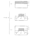
- Figs. 2, 3, 4 and 5 are cross-sectional views showing the steps of a method of fabricating the ferroelectric memory shown in Fig. 1.
- a gate insulating film 2 composed of SiO 2 having a thickness of 100 ⁇ is formed on a p-type silicon substrate 1 by a thermal oxidation method, and a first lower electrode 3 composed of polysilicon having a thickness of 2000 ⁇ is formed on the gate insulating film 2 by a CVD method (a chemical vapor deposition method).
- the first lower electrode 3 and the gate insulating film 2 in a portion excluding a gate forming region on the silicon substrate 1 are then removed using a dry process such as reactive-ion etching (RIE) or ion milling, to form a gate portion.
- RIE reactive-ion etching
- n-type impurities an n-type dopant
- a region of the silicon substrate 1 between the source region 4 and the drain region 5 is a channel region 6.
- an interlayer insulating film 7 composed of SiO 2 , etc. having a thickness of approximately 6000 ⁇ is formed by a CVD method or the like on the silicon substrate 1 so as to cover the first lower electrode 3 and the gate insulating film 2, as shown in Fig. 2 (c).
- a buffer layer 8 having a thickness of 500 ⁇ composed of TiO 2 , CeO 2 , etc. is then formed on the interlayer insulating film 7. Thereafter, a contact hole 9 is provided by a lithographic technique in the buffer layer 8 and the interlayer insulating film 7 on the first lower electrode 3, as shown in Fig. 3 (e).
- a connecting layer 10 composed of a conductive material such as polysilicon or W is formed in the contact hole 9.
- the thickness of the connecting layer 10 is set such that the distance from an upper end of the contact hole 9 to the upper surface of the connecting layer 10 is 1500 ⁇ .
- a conductive layer is formed on the inside of the contact hole 9 and the whole surface of the buffer layer 8, after which the whole surface is etched, to remove a conductive layer on the buffer layer 8.
- a diffusion barrier layer 11 composed of a conductive material such as TiN or TaSiN is then formed on the inside of the contact hole 9 and the whole surface of the buffer layser 8 by a sputtering method, a CVD method or the like in order to prevent the connecting layer 10 from being oxidized and prevent impurities from being diffused into a gate portion.
- the whole surface of the diffusion barrier layer 11 is etched, to remove the diffusion barrier layer 11 on the buffer layer 8 as well as to etch the buffer layer 11 back until the upper surface of the diffusion barrier layer 11 in the contact hole 9 is lower than the upper surface of the buffer layer 8.
- mixed gas of BCl 3 and Cl 2 is used as etching gas, and the etching conditions are an RF power of 250 W and a pressure of 2 ⁇ 10 -2 torr.
- the other gas such as Ar or N 2 may be mixed with the mixed gas.
- a diffusion barrier layer 11 having a thickness of 300 ⁇ is thus formed on the connecting layer 10 in the contact hole 9.
- the diffusion barrier layer 11 will be a part of the second lower electrode 12 formed in the subsequent process.
- a second lower electrode 12 having a thickness of 3000 ⁇ composed of a conductive material such as Pt or IrO 2 is then formed on the buffer layer 8 and the diffusion barrier layer 11 in the contact hole 9 by a sputtering method, a CVD method, a sol-gel method or the like.
- a sputtering method a sputtering method, a CVD method, a sol-gel method or the like.
- Another material on which a ferroelectric crystal can be grown may be used as a material for the second lower electrode 12.
- RuO x ruthenium oxide
- the second lower electrode 12 is then flattened by etch-back, a CMP method (a chemical mechanical polishing method) or the like, leaving the second lower electrode 12 in the contact hole 9, to form the second lower electrode 12 having a thickness of 1200 ⁇ in the contact hole 9.
- Cl 2 is used as etching gas
- the etching conditions are an RF power of 300 W and a pressure of 3 ⁇ 10 -3 torr.
- the etching gas the other gas such as Ar, HBr or BCl 3 may be used, or their mixed gas may be used.
- the second lower electrode 12 and the diffusion barrier layer 11 may be simultaneously flattened by etch-back or a CMP method after continuously forming the diffusion barrier layer 11 and the second lower electrode 12 instead of etching the diffusion barrier layer 11 back in the step shown in Fig. 4 (f).
- a ferroelectric thin film 13 having a thickness of 2000 ⁇ composed of PZT, SrBiTaO, etc. is then formed by a sol-gel method, a sputtering method, a CVD method or the like on the second lower electrode 12 and the buffer layer 8.
- an upper electrode 14 composed of a conductive material such as Pt or IrO 2 having a thickness of 1500 ⁇ is then formed by a sputtering method on the ferroelectric thin film 13.
- the upper electrode 14 and the ferroelectric thin film 13 are simultaneously patterned by etching, as shown in Fig. 6 (m).
- Cl 2 is used as etching gas
- the etching conditions are an RF power of 300 W and a pressure of 3 ⁇ 10 -3 torr.
- the etching gas the other gas such as Ar, CF 4 , SF 6 , HBr, or BCl 3 may be used, or their mixed gas may be used.
- the upper electrode 14 and the ferroelectric thin film 13 may be separately etched. At the time of etching, the whole of the buffer layer 8 may be etched.
- the ferroelectric thin film 13 need not necessarily extend over the buffer layer 8, provided that it is brought into contact with the upper surface of the second lower electrode 12.
- the buffer layer 8 and the interlayer insulating film 7 on the source electrode 4 and the buffer layer 8 and the interlayer insulating film 7 on the drain electrode 5 are then respectively provided with the contact holes, and a source electrode 15 and a drain electrode 16 composed of a conductive material such as polysilicon or tungsten are respectively formed in the contact holes, as shown in Fig. 1. Finally, wiring layers 17 and 18 composed of Al are respectively formed on the source electrode 15 and the drain electrode 16. A ferroelectric memory according to the present embodiment is thus fabricated.
- the second lower electrode 12 is provided in the contact hole 9 of the interlayer insulating film 7.
- the conductive material for the second lower electrode 12 does not adhere or deposit on sidewalls of the ferroelectric thin film 13. Even if the conductive material for the upper electrode 14 adheres or deposits on the sidewalls of the ferroelectric thin film 13, a current does not leak between the upper electrode 14 and the second lower electrode 12 because the second lower electrode 12 is provided in the contact hole 9 of the interlayer insulating film 7. As a result, the reliability and the yield of the ferroelectric memory are improved.
- the ferroelectric thin film 13 is formed on the interlayer insulating film 7 through the buffer layer 8, so that the stress applied to the ferroelectric thin film 13 is retrieved by the buffer layer 8. Therefore, the ferroelectric thin film 13 is prevented from being cracked, and constituent elements are prevented from reacting with each other (for example, reaction between Pb and SiO 2 ) and mutually diffusing between the ferroelectric thin film 13 and the interlayer insulating film 7. As a result, the reliability and the yield of the ferroelectric memory are further improved.
- the ferroelectric thin film 13 is formed on the second upper electrode 12 composed of a material which is low in reactivity, for example, Pt, and the interlayer insulating film 7 is provided between the ferroelectric thin film 13 and the silicon substrate 1, so that the constituent elements are sufficiently prevented from reacting with each other or mutually diffusing between the ferroelectric thin film 13 and the silicon substrate 1.
- the surface of the second lower electrode 12 with the ferroelectric thin film 13 is negatively charged, and the surface of the first lower electrode 3 with the gate insulating film 2 is positively charged.
- an inversion layer is formed in the channel region 6 between the source region 4 and the drain region 5, so that an FET is turned on, although the voltage of the upper electrode 14 is zero.
- the surface of the second lower electrode 12 with the ferroelectric thin film 13 is positively charged, and the surface of the first lower electrode 3 with the gate insulating film 2 is negatively charged.
- no inversion layer is formed in the channel region 6 between the source region 4 and the drain region 5, so that the FET is turned off.
- the FET When the ferroelectric thin film 13 is thus sufficiently polarized inversely, the FET can be selectively turned on or off even after a voltage applied to the upper electrode 14 is set to zero. Therefore, it is possible to discriminate between data "1" and "0" which are stored in the ferroelectric memory by detecting a current between a source and a drain.
- a voltage other than "0" by which the FET can be selectively turn on or off, may be applied to the upper electrode 14.
- ferroelectric thin film 13 ferroelectrics composed of the following materials may be used.
- a molecular beam epitaxy (MBE) method As a method of forming the ferroelectric thin film 13, a molecular beam epitaxy (MBE) method, a laser ablation method, a laser molecular beam epitaxy method, a sputtering method (of an RF (Radio Frequency) type, a DC (Direct Current) type, or an ion beam type), a reactive evaporation method, an MOCVD method (a metal organic chemical vapor deposition method), a mist deposition method, a sol-gel method, etc. can be used depending on the above-mentioned material for the ferroelectric thin film 13.
- MBE molecular beam epitaxy
- a material for the second lower electrode 12 and the upper electrode 14 are not limited to Pt or IrO 2 .
- the other material may be used. Examples include noble metals (Au, Ag, Pt, Ru, Rh, Pb, Os, Ir, etc.), high-melting point metals (Co, W, Ti, etc.), high-melting point metal compounds (TiN, IrSiN, etc.), conductive oxides (RuO 2 , RhO 2 , OsO 2 , IrO 2 , ReO 2 , ReO 3 , MoO 2 , WO 2 , SrRuO 3 , Pb 2 RuO 3-X , Bi 2 Ru 2 O 7-X , etc.), or alloys of the materials.
- the second lower electrode 12 and the upper electrode 14 may have a multilayer structure of the above-mentioned materials, or a two-layer structure in which a Pt layer is formed on a Ti layer, for example.
- Materials for the first lower electrode 3 and the connecting layer 10 are not limited to polysilicon or W. Other conductive materials may be used.
- the FET is formed on the silicon substrate 1, the FET may be formed on the other semiconductor substrate or semiconductor layer.
- ferroelectric memory having an n-type channel Although description was made of the ferroelectric memory having an n-type channel, a ferroelectric memory having a p-type channel is also realized by reversing the conductivity type of each layer.
- one contact hole 9 is provided in the interlayer insulating film 7 on the first lower electrode 3
- a plurality of contact holes may be formed in the interlayer insulating film 7 on the first lower electrode 3 so that second lower electrodes in the contact holes are brought into contact with the ferroelectric thin film 13.
- one ferroelectric thin film may be shared by a plurality of FETs so that the ferroelectric thin film is brought into contact with second lower electrodes in a plurality of contact holes provided in upper parts of the plurality of FETs.
- the present invention is also applicable to a ferroelectric memory which performs nonvolatile operations. Further, the present invention is also applicable to another dielectric device such as a capacitor having a structure in which a conductive layer is brought into contact with a dielectric film.
Landscapes
- Semiconductor Memories (AREA)
- Non-Volatile Memory (AREA)
- Semiconductor Integrated Circuits (AREA)
Applications Claiming Priority (2)
| Application Number | Priority Date | Filing Date | Title |
|---|---|---|---|
| JP158809/97 | 1997-06-16 | ||
| JP15880997A JP3281839B2 (ja) | 1997-06-16 | 1997-06-16 | 誘電体メモリおよびその製造方法 |
Publications (2)
| Publication Number | Publication Date |
|---|---|
| EP0886317A2 true EP0886317A2 (de) | 1998-12-23 |
| EP0886317A3 EP0886317A3 (de) | 1999-02-17 |
Family
ID=15679840
Family Applications (1)
| Application Number | Title | Priority Date | Filing Date |
|---|---|---|---|
| EP98304720A Ceased EP0886317A3 (de) | 1997-06-16 | 1998-06-15 | Ferroelektrische Vorrichtung, nichtflüchtiger Halbleiterspeicher und Verfahren zu ihrer Herstellung |
Country Status (3)
| Country | Link |
|---|---|
| US (1) | US6194752B1 (de) |
| EP (1) | EP0886317A3 (de) |
| JP (1) | JP3281839B2 (de) |
Cited By (8)
| Publication number | Priority date | Publication date | Assignee | Title |
|---|---|---|---|---|
| EP0923117A1 (de) * | 1997-12-04 | 1999-06-16 | Sharp Kabushiki Kaisha | Herstellungsverfahren von einer Speicherzelle mit ferroelektrischem Einzeltransistor unter Verwendung eines chemisch-mechanischem Polierverfahren |
| EP1006590A1 (de) * | 1998-12-01 | 2000-06-07 | Rohm Co., Ltd. | Ferroelektrischer Speicher und Verfahren zur Herstellung |
| WO2000049660A1 (en) * | 1999-02-16 | 2000-08-24 | Symetrix Corporation | Iridium oxide diffusion barrier between local interconnect layer and thin film of layered superlattice material |
| DE10009762A1 (de) * | 2000-03-01 | 2001-09-20 | Infineon Technologies Ag | Herstellungsverfahren für einen Speicherkondensator mit einem Dielektrikum auf der Basis von Strontium-Wismut-Tantalat |
| EP1102329A3 (de) * | 1999-11-17 | 2003-09-24 | Sanyo Electric Co., Ltd. | Dielektrisches Element |
| US6762476B2 (en) | 2001-02-06 | 2004-07-13 | Sanyo Electric Co., Ltd | Dielectric element including oxide dielectric film and method of manufacturing the same |
| US6888189B2 (en) | 2000-11-08 | 2005-05-03 | Sanyo Electric Co., Ltd. | Dielectric element including oxide-based dielectric film and method of fabricating the same |
| EP1657738A2 (de) | 1999-02-04 | 2006-05-17 | Rohm Co., Ltd. | Kondensator und dessen Herstellungsverfahren |
Families Citing this family (16)
| Publication number | Priority date | Publication date | Assignee | Title |
|---|---|---|---|---|
| JP3171170B2 (ja) * | 1998-05-25 | 2001-05-28 | 日本電気株式会社 | 薄膜キャパシタおよびその製造方法 |
| JP2000349249A (ja) * | 1999-06-08 | 2000-12-15 | Oki Electric Ind Co Ltd | 半導体記憶装置の製造方法 |
| US6495878B1 (en) * | 1999-08-02 | 2002-12-17 | Symetrix Corporation | Interlayer oxide containing thin films for high dielectric constant application |
| DE60021041T2 (de) * | 1999-10-13 | 2006-05-04 | Rohm Co. Ltd. | Nichtflüchtiger Speicher und Steuerungsverfahren dafür |
| KR100612561B1 (ko) * | 2000-06-19 | 2006-08-11 | 주식회사 하이닉스반도체 | 반도체 소자의 캐패시터 제조 방법 |
| US20020109166A1 (en) * | 2001-02-13 | 2002-08-15 | Hsu Sheng Teng | MFMOS/MFMS non-volatile memory transistors and method of making same |
| US6531324B2 (en) * | 2001-03-28 | 2003-03-11 | Sharp Laboratories Of America, Inc. | MFOS memory transistor & method of fabricating same |
| US6566148B2 (en) * | 2001-08-13 | 2003-05-20 | Sharp Laboratories Of America, Inc. | Method of making a ferroelectric memory transistor |
| DE10212962B4 (de) * | 2002-03-22 | 2007-11-29 | Qimonda Ag | Halbleiterspeicherzelle mit Zugriffstransistor auf der Grundlage eines organischen Halbleitermaterials und Halbleiterspeichereinrichtung |
| US6531325B1 (en) * | 2002-06-04 | 2003-03-11 | Sharp Laboratories Of America, Inc. | Memory transistor and method of fabricating same |
| DE10308970A1 (de) * | 2003-02-28 | 2004-09-09 | Infineon Technologies Ag | Halbleiterspeicherzelle und Verfahren zu deren Herstellung |
| DE10333557B8 (de) * | 2003-07-23 | 2008-05-29 | Qimonda Ag | Verfahren zur Herstellung einer Speichereinrichtung, Speicherzelle, Speichereinrichtung und Verfahren zum Betrieb der Speichereinrichtung |
| KR100543528B1 (ko) * | 2003-08-26 | 2006-01-31 | 한국과학기술연구원 | 식각 선택비가 큰 버퍼층을 이용한 자기정렬 강유전체게이트 트랜지스터의 제조방법 |
| KR100823168B1 (ko) * | 2007-01-08 | 2008-04-18 | 삼성전자주식회사 | 강유전체 메모리 장치 및 그 형성 방법 |
| US9773793B2 (en) * | 2009-10-09 | 2017-09-26 | Texas Instuments Incorporated | Transistor performance modification with stressor structures |
| US10937783B2 (en) | 2016-11-29 | 2021-03-02 | Taiwan Semiconductor Manufacturing Co., Ltd. | Semiconductor device and manufacturing method thereof |
Family Cites Families (4)
| Publication number | Priority date | Publication date | Assignee | Title |
|---|---|---|---|---|
| JPH05327062A (ja) * | 1992-05-22 | 1993-12-10 | Sharp Corp | 強誘電体記憶素子 |
| US5585300A (en) | 1994-08-01 | 1996-12-17 | Texas Instruments Incorporated | Method of making conductive amorphous-nitride barrier layer for high-dielectric-constant material electrodes |
| JP2982855B2 (ja) * | 1994-09-20 | 1999-11-29 | 日本電気株式会社 | 半導体装置とその製造方法 |
| US5731608A (en) * | 1997-03-07 | 1998-03-24 | Sharp Microelectronics Technology, Inc. | One transistor ferroelectric memory cell and method of making the same |
-
1997
- 1997-06-16 JP JP15880997A patent/JP3281839B2/ja not_active Expired - Fee Related
-
1998
- 1998-06-15 EP EP98304720A patent/EP0886317A3/de not_active Ceased
- 1998-06-15 US US09/094,592 patent/US6194752B1/en not_active Expired - Fee Related
Cited By (13)
| Publication number | Priority date | Publication date | Assignee | Title |
|---|---|---|---|---|
| EP0923117A1 (de) * | 1997-12-04 | 1999-06-16 | Sharp Kabushiki Kaisha | Herstellungsverfahren von einer Speicherzelle mit ferroelektrischem Einzeltransistor unter Verwendung eines chemisch-mechanischem Polierverfahren |
| US6900486B1 (en) | 1998-12-01 | 2005-05-31 | Rohm Co., Ltd. | Ferroelectric memory and method for manufacturing same |
| EP1006590A1 (de) * | 1998-12-01 | 2000-06-07 | Rohm Co., Ltd. | Ferroelektrischer Speicher und Verfahren zur Herstellung |
| US6656747B2 (en) | 1998-12-01 | 2003-12-02 | Rohm Co., Ltd. | Ferroelectric memory and method for manufacturing same |
| EP1657738A3 (de) * | 1999-02-04 | 2006-08-30 | Rohm Co., Ltd. | Kondensator und dessen Herstellungsverfahren |
| EP1657738A2 (de) | 1999-02-04 | 2006-05-17 | Rohm Co., Ltd. | Kondensator und dessen Herstellungsverfahren |
| WO2000049660A1 (en) * | 1999-02-16 | 2000-08-24 | Symetrix Corporation | Iridium oxide diffusion barrier between local interconnect layer and thin film of layered superlattice material |
| EP1102329A3 (de) * | 1999-11-17 | 2003-09-24 | Sanyo Electric Co., Ltd. | Dielektrisches Element |
| US6720096B1 (en) | 1999-11-17 | 2004-04-13 | Sanyo Electric Co., Ltd. | Dielectric element |
| DE10009762A1 (de) * | 2000-03-01 | 2001-09-20 | Infineon Technologies Ag | Herstellungsverfahren für einen Speicherkondensator mit einem Dielektrikum auf der Basis von Strontium-Wismut-Tantalat |
| DE10009762B4 (de) * | 2000-03-01 | 2004-06-03 | Infineon Technologies Ag | Herstellungsverfahren für einen Speicherkondensator mit einem Dielektrikum auf der Basis von Strontium-Wismut-Tantalat |
| US6888189B2 (en) | 2000-11-08 | 2005-05-03 | Sanyo Electric Co., Ltd. | Dielectric element including oxide-based dielectric film and method of fabricating the same |
| US6762476B2 (en) | 2001-02-06 | 2004-07-13 | Sanyo Electric Co., Ltd | Dielectric element including oxide dielectric film and method of manufacturing the same |
Also Published As
| Publication number | Publication date |
|---|---|
| US6194752B1 (en) | 2001-02-27 |
| JPH118356A (ja) | 1999-01-12 |
| JP3281839B2 (ja) | 2002-05-13 |
| EP0886317A3 (de) | 1999-02-17 |
Similar Documents
| Publication | Publication Date | Title |
|---|---|---|
| US6194752B1 (en) | Dielectric device, dielectric memory and method of fabricating the same | |
| US5638319A (en) | Non-volatile random access memory and fabrication method thereof | |
| US6974985B2 (en) | Capacitor and method for fabricating the same, and semiconductor device and method for fabricating the same | |
| US6534326B1 (en) | Method of minimizing leakage current and improving breakdown voltage of polycrystalline memory thin films | |
| CA2225681C (en) | Barrier layer for ferroelectric capacitor integrated on silicon | |
| US7405121B2 (en) | Semiconductor device with capacitors and its manufacture method | |
| US6858492B2 (en) | Method for fabricating a semiconductor memory device | |
| US6291292B1 (en) | Method for fabricating a semiconductor memory device | |
| JP2003068993A (ja) | 半導体装置およびその製造方法 | |
| US20100252867A1 (en) | MFMS-FET, Ferroelectric Memory Device, And Methods Of Manufacturing The Same | |
| JP2001127262A (ja) | 強誘電体キャパシタ、その製造方法、および半導体装置 | |
| US7153706B2 (en) | Ferroelectric capacitor having a substantially planar dielectric layer and a method of manufacture therefor | |
| US20080160642A1 (en) | Semiconductor device | |
| KR100209748B1 (ko) | 반도체 장치의 축전기 제조방법 | |
| KR0155866B1 (ko) | 강유전체 메모리 장치 및 그 제조 방법 | |
| US8318560B2 (en) | Methods of forming integrated circuit devices including a capacitor | |
| JPH1168057A (ja) | 誘電体素子 | |
| JP4095582B2 (ja) | 半導体装置及びその製造方法 | |
| JPH113976A (ja) | 誘電体素子、強誘電体メモリおよびその動作方法 | |
| JPH118362A (ja) | 誘電体素子、誘電体メモリ、誘電体メモリの製造方法および強誘電体メモリの動作方法 | |
| JP2000150813A (ja) | 半導体装置及び半導体装置の製造方法 | |
| JP2000174228A (ja) | 半導体集積回路及びその製造方法 | |
| US7527984B2 (en) | Semiconductor device | |
| JPH10341003A (ja) | 誘電体素子およびその製造方法 | |
| JPH10270651A (ja) | 半導体記憶装置 |
Legal Events
| Date | Code | Title | Description |
|---|---|---|---|
| PUAI | Public reference made under article 153(3) epc to a published international application that has entered the european phase |
Free format text: ORIGINAL CODE: 0009012 |
|
| AK | Designated contracting states |
Kind code of ref document: A2 Designated state(s): DE FR GB |
|
| AX | Request for extension of the european patent |
Free format text: AL;LT;LV;MK;RO;SI |
|
| PUAL | Search report despatched |
Free format text: ORIGINAL CODE: 0009013 |
|
| RIN1 | Information on inventor provided before grant (corrected) |
Inventor name: ISHIZUKA, YOSHIYUKI Inventor name: GUESHI, TATSURO Inventor name: GOTO, TAKASHI Inventor name: FURUKAWA, HIROAKI Inventor name: HARADA, MITSUAKI Inventor name: OGASAHARA, SATORU |
|
| AK | Designated contracting states |
Kind code of ref document: A3 Designated state(s): AT BE CH CY DE DK ES FI FR GB GR IE IT LI LU MC NL PT SE |
|
| AX | Request for extension of the european patent |
Free format text: AL;LT;LV;MK;RO;SI |
|
| RTI1 | Title (correction) | ||
| 17P | Request for examination filed |
Effective date: 19990607 |
|
| AKX | Designation fees paid |
Free format text: DE FR GB |
|
| 17Q | First examination report despatched |
Effective date: 19991103 |
|
| RIC1 | Information provided on ipc code assigned before grant |
Free format text: 7H 01L 27/115 A, 7H 01L 21/02 B |
|
| GRAG | Despatch of communication of intention to grant |
Free format text: ORIGINAL CODE: EPIDOS AGRA |
|
| RIC1 | Information provided on ipc code assigned before grant |
Free format text: 7H 01L 27/115 A, 7H 01L 21/8246 B, 7H 01L 21/02 B |
|
| RTI1 | Title (correction) |
Free format text: DIELECTRIC MEMORY AND METHOD OF FABRICATING THE SAME |
|
| STAA | Information on the status of an ep patent application or granted ep patent |
Free format text: STATUS: THE APPLICATION HAS BEEN REFUSED |
|
| 18R | Application refused |
Effective date: 20020721 |