EP0905064B1 - Förderer für gegenstände - Google Patents
Förderer für gegenstände Download PDFInfo
- Publication number
- EP0905064B1 EP0905064B1 EP98900208A EP98900208A EP0905064B1 EP 0905064 B1 EP0905064 B1 EP 0905064B1 EP 98900208 A EP98900208 A EP 98900208A EP 98900208 A EP98900208 A EP 98900208A EP 0905064 B1 EP0905064 B1 EP 0905064B1
- Authority
- EP
- European Patent Office
- Prior art keywords
- transport
- air
- terminal end
- transport direction
- passage
- Prior art date
- Legal status (The legal status is an assumption and is not a legal conclusion. Google has not performed a legal analysis and makes no representation as to the accuracy of the status listed.)
- Expired - Lifetime
Links
- 230000007246 mechanism Effects 0.000 claims description 28
- 230000003247 decreasing effect Effects 0.000 claims description 11
- 230000032258 transport Effects 0.000 description 275
- 239000004065 semiconductor Substances 0.000 description 103
- 238000000034 method Methods 0.000 description 12
- NJPPVKZQTLUDBO-UHFFFAOYSA-N novaluron Chemical compound C1=C(Cl)C(OC(F)(F)C(OC(F)(F)F)F)=CC=C1NC(=O)NC(=O)C1=C(F)C=CC=C1F NJPPVKZQTLUDBO-UHFFFAOYSA-N 0.000 description 12
- 238000004519 manufacturing process Methods 0.000 description 8
- 230000014759 maintenance of location Effects 0.000 description 3
- 229910052751 metal Inorganic materials 0.000 description 3
- 239000002184 metal Substances 0.000 description 3
- 239000000919 ceramic Substances 0.000 description 2
- 230000000694 effects Effects 0.000 description 2
- 239000011521 glass Substances 0.000 description 2
- 238000007689 inspection Methods 0.000 description 2
- 238000003754 machining Methods 0.000 description 2
- 238000004080 punching Methods 0.000 description 2
- 238000000926 separation method Methods 0.000 description 2
- 238000003860 storage Methods 0.000 description 2
- 239000004593 Epoxy Substances 0.000 description 1
- 229910052581 Si3N4 Inorganic materials 0.000 description 1
- 229910052782 aluminium Inorganic materials 0.000 description 1
- XAGFODPZIPBFFR-UHFFFAOYSA-N aluminium Chemical compound [Al] XAGFODPZIPBFFR-UHFFFAOYSA-N 0.000 description 1
- 230000015572 biosynthetic process Effects 0.000 description 1
- 238000007599 discharging Methods 0.000 description 1
- 238000005553 drilling Methods 0.000 description 1
- 229910052745 lead Inorganic materials 0.000 description 1
- 239000000463 material Substances 0.000 description 1
- 150000002739 metals Chemical class 0.000 description 1
- 229910002077 partially stabilized zirconia Inorganic materials 0.000 description 1
- 239000011148 porous material Substances 0.000 description 1
- 238000003672 processing method Methods 0.000 description 1
- 239000011347 resin Substances 0.000 description 1
- 229920005989 resin Polymers 0.000 description 1
- HQVNEWCFYHHQES-UHFFFAOYSA-N silicon nitride Chemical compound N12[Si]34N5[Si]62N3[Si]51N64 HQVNEWCFYHHQES-UHFFFAOYSA-N 0.000 description 1
- 239000007787 solid Substances 0.000 description 1
- 239000000758 substrate Substances 0.000 description 1
Images



Classifications
-
- H—ELECTRICITY
- H05—ELECTRIC TECHNIQUES NOT OTHERWISE PROVIDED FOR
- H05K—PRINTED CIRCUITS; CASINGS OR CONSTRUCTIONAL DETAILS OF ELECTRIC APPARATUS; MANUFACTURE OF ASSEMBLAGES OF ELECTRICAL COMPONENTS
- H05K13/00—Apparatus or processes specially adapted for manufacturing or adjusting assemblages of electric components
- H05K13/02—Feeding of components
- H05K13/027—Fluid transport of components
-
- Y—GENERAL TAGGING OF NEW TECHNOLOGICAL DEVELOPMENTS; GENERAL TAGGING OF CROSS-SECTIONAL TECHNOLOGIES SPANNING OVER SEVERAL SECTIONS OF THE IPC; TECHNICAL SUBJECTS COVERED BY FORMER USPC CROSS-REFERENCE ART COLLECTIONS [XRACs] AND DIGESTS
- Y10—TECHNICAL SUBJECTS COVERED BY FORMER USPC
- Y10S—TECHNICAL SUBJECTS COVERED BY FORMER USPC CROSS-REFERENCE ART COLLECTIONS [XRACs] AND DIGESTS
- Y10S414/00—Material or article handling
- Y10S414/10—Associated with forming or dispersing groups of intersupporting articles, e.g. stacking patterns
- Y10S414/101—Associated with forming or dispersing groups of intersupporting articles, e.g. stacking patterns with article-supporting fluid cushion
Definitions
- the present invention relates to an object transport apparatus for transporting an object (various electronic parts such as semiconductor chips) placed in a production process to the next production step, or for transporting a completed object to the next assembling step.
- a container which is composed of a box with an open top, is often used in the production line for an object (various electronic parts such as semiconductor chips), in order to transport a large number of electronic parts to the next processing step or to a storage chamber or the like.
- workpieces For example, when a large number of electronic parts or the like (hereinafter simply referred to as "workpieces”) are transported by using the container in the production line, then the large number of workpieces are randomly introduced into the container, and they are automatically transported to the next processing step or to the storage chamber by using, for example, a belt conveyer and a transport arm.
- a method which is used when the object, which is subjected to the transport, has a small size, for example, when the object is a semiconductor chip.
- a transport passage is provided with a large number of holes, and air is discharged through the large number of holes to transport the object.
- this method a large number of small-sized objects can be smoothly transported. Therefore, this method is advantageous to shorten the time required to perform the transport.
- Transport apparatus operating by such a method is disclosed in JP-A-07-80011 and JP-A-06-9052.
- the conventional transport apparatus based on the use of air merely transports the objects in one direction by discharging air. Therefore, an inconvenience arises in that the objects are closely contacted with each other at the terminal end of the transport passage in the transport direction, and it is difficult to pick up the object which has arrived at the terminal end.
- the present invention has been made taking such problems into consideration, an object of which is to provide a transport system for transporting an object in one direction while floating the object by means of air, especially an object transport apparatus which makes it possible to realize automatic operation to pick up individual objects one by one.
- an object transport apparatus provided with at least one line of groove for constructing a transport passage for transporting an object, the object transport apparatus comprising a mechanism for moving the object in a transport direction, a floating mechanism, and a floating-accelerating mechanism disposed at a terminal end in the transport direction.
- the floating mechanism for the object is operated so that a large number of objects, which are placed on the object transport surface, are slightly floated upwardly.
- the mechanism for moving the object in the transport direction is operated.
- the large number of objects are transported together toward the downstream side in the transport direction.
- the floating-accelerating mechanism for the object is provided at the terminal end in the transport direction. Therefore, the object, which has arrived at the terminal end of the transport passage in the transport direction, is positioned in a state in which the concerning object is floated to a position higher than those of the other objects. Accordingly, the object, which is positioned at the terminal end in the transport direction, can be easily picked up without using any manual operation. It is possible to realize automatic operation for picking up a large number of transported individual objects one by one. This results in fully automatic operation for the entire object transport system.
- the mechanism for moving the object in the transport direction comprises any one of, or a combination of a means for inclining the transport passage downwardly by a predetermined angle toward the transport direction, a large number of air-jetting holes which are formed through a transport surface of the transport passage so that air is jetted toward the transport direction, and a pushing means provided toward the transport direction at a starting end of the transport passage in the transport direction.
- the use of the means for inclining the transport passage downwardly by the predetermined angle toward the transport direction allows the large number of objects to be transported in accordance with their own weights to the downstream side in the transport direction.
- the angle of inclination is preferably not more than 2°. If the angle of inclination is too small, the ability to transport the object is deteriorated. Therefore, the angle of inclination is preferably not less than 0.5°.
- the large number of objects are transported toward the downstream side in the transport direction by allowing the large number of air-jetting holes to penetrate through the transport surface of the transport passage so that air is jetted toward the transport direction, or by providing the pushing means toward the transport direction at the starting end of the transport passage in the transport direction.
- the "air-jetting holes" referred to herein indicate a large number of through-holes which are formed mechanically, and a large number of holes of a porous material such as sintered metal.
- the jetting angle of the air-jetting holes provided through the transport surface may be determined to be an appropriate angle considering the shape and the weight of the object in view of the balance with the ability as an object-floating mechanism as described later on.
- the air-jetting holes may also serve as the object-floating mechanism, and hence it is possible to reduce the cost owing to the simplification of the apparatus. Further, it is possible to simplify the handling operation for the apparatus, and it is possible to improve the reliability of the apparatus.
- a method based on the use of air discharge, or a mechanical pushing method such as those based on the use of a piston may be appropriately selected and used as the pushing means. Accordingly, it is possible to control the transport ability in an independent manner.
- the applicable range of the operating condition including, for example, the shape of the object and the transport speed is expanded. Especially, it is possible to dissolve the trouble which would be otherwise caused such that the object is sunk without being floated at the starting end of the transport passage at which the object is introduced.
- the floating mechanism has a large number of air-jetting holes which are formed through an object transport surface of the transport passage.
- the air is jetted upwardly from the air-jetting holes in a direction perpendicular to the transport surface.
- the floating-accelerating mechanism may appropriately select and use any one of, or a combination of a means for allowing a planar configuration of the transport passage to have a shape for maximizing a floating amount of the object at the terminal end in the transport direction, and a means with a large number of air-jetting holes which are formed through an object transport surface of the transport passage for increasing an air-jetting amount of the air-jetting holes of the large number of air-jetting holes disposed at the terminal end in the transport direction as compared with an air-jetting amount of the air-jetting holes disposed at positions other than the terminal end in the transport direction.
- the object which has arrived at the terminal end of the transport passage in the transport direction, is in a state of being floated higher than the other objects, and the object is positioned highly accurately.
- the air-jetting amount of the air-jetting holes disposed at the terminal end in the transport direction is increased as compared with the air-jetting amount of the air-jetting holes disposed at the positions other than the terminal end in the transport direction.
- the following methods are available to increase the air-jetting amount at the terminal end in the transport direction. That is, the number of the air-jetting holes is increased as compared with those for the portions other than the terminal end in the transport direction. Alternatively, the air-jetting amount per one air-jetting hole is increased.
- the grooves for forming the object transport passages are provided in parallel to one another in a number of lines corresponding to quality levels of the objects.
- the objects are introduced into the respective grooves corresponding to the quality levels acknowledged for each of the objects in the previous step (for example, in the inspection step). Accordingly, the objects of approximately the same quality level can be gathered in each of the transport passages.
- a certain apparatus or device can be assembled by using the objects each having approximately the same quality transported via one transport passage. Therefore, it is possible to improve the quality of the apparatus or device.
- the air-jetting holes are provided at three points or more with respect to a projected area of the object. Accordingly, all of the large number of objects placed on the transport passage can be floated without any fluctuation. Thus, it is possible to avoid retention of the objects on the transport passage. That is, all of the large number of objects can be efficiently transported in the transport direction.
- the transport passage has a planar configuration in which a clearance area is decreased stepwise in the transport direction provided that the clearance area is an area obtained by subtracting a projected area of the object from an area of an object transport surface of the transport passage. Accordingly, the larger the clearance area is, the more easily the air jetted from the air-jetting holes tends to leak through the clearance. Therefore, the floating amount of the object is decreased. On the contrary, the smaller the clearance area is, the more difficultly the air jetted from the air-jetting holes tends to leak through the clearance. Therefore, the floating amount of the object is increased.
- the clearance area is decreased stepwise in the transport direction. Accordingly, the floating amount is increased as the object is moved to the downstream in the transport direction. The floating amount of the object is maximized when the object arrives at the terminal end in the transport direction.
- a slit is provided through a terminal end wall of the transport passage in the transport direction. Accordingly, a part of the air discharged from the air-jetting holes leaks at the terminal end in the transport direction through the slit toward the outside of the transport passage in the transport direction and in the upward direction. Thus, it is possible to adjust the floating amount of the object, and it is possible to smoothly move (transport) the object in the transport direction. Further, it is possible to dissolve the problem which would be otherwise caused such that the terminal end wall in the transport direction is in a state of so-called drift in which foreign matters are deposited, and the foreign matters adhere to the object which collides with the terminal end wall.
- the transport condition can be individually adjusted by changing the condition of slit formation for each of the transport passages.
- a projection is provided on a terminal end wall of the transport passage in the transport direction.
- the terminal end of the transport passage is formed by a side wall
- the object which has arrived at the terminal end portion in the transport direction, makes surface-to-surface contact with the terminal end wall. Therefore, in order to decrease the inclination of the object located at the terminal end portion in the transport direction so that the object is floated, it is necessary that the air-jetting force exerted on the object is not less than the contact frictional force of the surface-to-surface contact. Considering the balance with respect to the floating amount of the object under the transport process, it is feared that the adjustment for the air-jetting amount may be difficult.
- the projection is provided on the terminal end wall in the transport direction. Therefore, the object, which has arrived at the terminal end portion in the transport direction, abuts against the projection in point-to-point contact or in line-to-line contact therewith. Accordingly, it is possible to decrease the air-jetting force exerted on the object, and it is easy, for example, to adjust the air-jetting amount. Further, the adhesion of foreign matters to the object also disappears.
- a projection is provided at a rear end of the object in the transport direction. Accordingly, the object, which has arrived at the terminal end in the transport direction, abuts against the projection formed on the terminal end wall in the transport direction, and the object abuts against the following object, in point-to-point contact or in line-to-line contact therewith. Therefore, the air-jetting force exerted on the object can be further decreased. Thus, it is possible to realize simplification of the control system and the structure of the air-jetting mechanism.
- the object is an electronic part.
- the present invention when the large number of objects are transported in the same direction, only the object, which is located at the terminal end in the transport direction, is floated to be higher than the other objects. Therefore, it is extremely easy to pick up the individual objects one by one. As a result, the present invention is sufficiently applicable when the object is the electronic part. Thus, it is possible to realize simplification of the semiconductor production steps, and it is possible to realize the fully automatic operation.
- a length of the object along the transport direction is continuously decreased in a direction of its height.
- the line-to-line contact is made between the concerning object and the terminal end wall and between the concerning object and the following object respectively.
- the rear end of the concerning object is moved along the tapered surface (the surface which is upwardly inclined in a direction to make separation from the terminal end in the transport direction) disposed at the front end of the following object.
- the object located at the terminal end in the transport direction is floated upwardly, the following object is moved while making advance into the space under the object located at the terminal end in the transport direction.
- the object located at the terminal end in the transport direction is floated upwardly easier than the other objects.
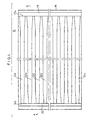
- the transport apparatus 10 comprises a main apparatus body 14 formed with a plurality of grooves in parallel to one another for constructing transport passages 12 for transporting a large number of semiconductor chips, a base pedestal 16 for supporting the main apparatus body 14 in a state of being inclined by a predetermined angle with respect to the transport direction, a starting end wall 18 having a prism-shaped configuration provided commonly for starting end openings 12a of the plurality of transport passages 12 of the main apparatus body 14, and a terminal end wall 20 also having a prism-shaped configuration provided commonly for terminal end openings 12b of the plurality of transport passages 12 of the main apparatus body 14.
- Those appropriately selected and adopted as the material for constructing the main apparatus body 14 include, for example, metals such as aluminum, resin substrates such as glass epoxy, ceramics such as ceramic partially stabilized zirconia and silicon nitride, and glass. When the metal is used, it is preferable to use those having flatness and less warpage, and it is preferable to use those having a large Young's modulus.
- Those appropriately usable as the processing method include, for example, plastic working, laser beam machining, electric discharge machining, punching processing based on punching, and processing based on drilling. As shown in FIG.
- the starting end wall 18 and the terminal end wall 20 are fixed on the base pedestal 16 by using, for example, a plurality of screws 22 screwed from the side of the bottom surface of the base pedestal 16.
- a placing surface for the main apparatus body 14 is defined by mutually opposing surfaces of the starting end wall 18 and the terminal end wall 20 and an upper surface of the base pedestal 16.
- the main apparatus body 14 is placed on the placing surface defined on the upper surface of the base pedestal 16.
- the main apparatus body 14 is fixed on the base pedestal 16 by means of screws 24 screwed from the side of the bottom surface of the base pedestal 16.
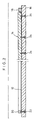
- the main apparatus body 14 is supported, for example, at an angle of inclination of 1° with respect to the placing surface (transport surface) of the base pedestal 16 by appropriately adjusting the screwing amount of the screw 24 screwed into the main apparatus body 14.
- the portion of the starting end opening 12a of the transport passage 12 (hereinafter simply referred to as “starting end Pa") is lifted upwardly with respect to the base pedestal 16.
- the portion of the terminal end opening 12b of the transport passage 12 (hereinafter simply referred to as “terminal end Pb”) is supported to make contact with the placing surface of the base pedestal 16.
- the planar configuration of each of the transport passages 12 is formed such that the configuration of the groove width is changed in a stepwise manner from the starting end Pa to the terminal end Pb.
- the width d1 is constant and smallest in an interval (region) K1 corresponding to a length which is 1.5 times as long as a length Lc of one chip in the direction from the terminal end Pb toward the starting end Pa.
- the width dx in an interval (region) K2 corresponding to the next length of about 20 mm is set to make continuous change to become wider toward the starting end Pa.
- the width dx is designed to become wider by a predetermined length t (about 0.4 mm) on both sides respectively over the interval K2.
- the width d1 of the interval K1 is set to be the minimum (in a degree of being slightly larger than the width of the semiconductor chip 28) as described above.
- the trouble is dissolved, which would be otherwise caused, for example, such that the semiconductor chips 28 meander, and they are caught by the side wall and the terminal end wall of the transport passage 12.
- the length of the interval K1 is set to be 1.5 times as long as the length Lc of one chip, and the interval K2 is provided in which the width dx is gradually enlarged.
- the semiconductor chips 28 can be floated gradually one by one, and it is possible to avoid the overlap of the semiconductor chips 28.
- the transport passage 12 is set such that the width dy is continuously widened in an interval K3 ranging from a point separated by a predetermined distance from the starting end Pa toward the terminal end Pb, to the starting end Pa.
- the increasing ratio of the width dy in the interval K3 is larger than the increasing ratio in the interval K2, giving a structure in which the semiconductor chip 28 is easily received. Therefore, when the semiconductor chip 28 is introduced into each of the transport passages 12, it is unnecessary to perform highly accurate positional control for a transport arm used to introduce the semiconductor chip 28 into the transport apparatus 10. Thus, it is sufficient to use a simple mechanism and a simple circuit system.
- the stepwise change of the groove width of each of the transport passages 12 in the main apparatus body 14 may be appreciated as shown in FIG. 4 on the basis of the aperture area with respect to the chip length Lc on the transport passage 12. That is, the aperture area in a range of one chip length Lc from the terminal end Pb, i.e., the aperture area for the first chip as counted from the terminal end Pb is not less than about 1.38 mm 2 . The aperture area for the next one chip length Lc (aperture area for the second chip) is not less than about 2.740 mm 2 . Similarly, the respective aperture areas for the third chip and the fourth chip are not less than 6.75 mm 2 and not less than 10.75 mm 2 respectively. The aperture areas for the fourth chip and the followings are approximately the same up to the point of start of the interval K3.
- the transport passage 12 has a planar configuration in which the clearance area is decreased stepwise in the transport direction provided that the clearance area is an area obtained by subtracting the projected area of the semiconductor chip 28 from the aperture area for the chip length Lc of the groove bottom surface.
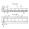
- the clearance distance ⁇ We (see FIG. 5B), for example, at a point e in the vicinity of the terminal end Pb in FIG. 3 is narrower than the clearance distance ⁇ Wn (see FIG. 5A), for example, at a point n in the vicinity of the starting end Pa.
- a large number of air-jetting holes 26 are formed through the groove bottom surface (chip transport surface) of each of the transport passages 12.
- the air-jetting holes 26 are provided at not less than three points for the projected area of the semiconductor chip 28. In the embodiment of the present invention, the air-jetting holes 26 are provided at five points for the projected area of the semiconductor chip 28. Specifically, as shown in FIG. 3, for example, assuming that the projected configuration of one chip (indicated by broken lines c) is a rectangular configuration, the air-jetting holes 26 are provided at portions corresponding to the four corners and at a portion corresponding to the center. In the embodiment of the present invention, the air-jetting hole 26 has a diameter of 0.2 mm.
- the air is discharged through the large number of air-jetting holes 26 provided through the groove bottom surface of the transport passage 12. Accordingly, the large number of semiconductor chips 28 introduced into the transport passage 12 are slightly floated upwardly. In this situation, the transport passage 12 is inclined downwardly by the predetermined angle (1° in this embodiment) toward the transport direction. Therefore, the large number of semiconductor chips 28 are transported together to the downstream side in the transport direction owing to their own weights.
- the planar configuration is given in which the groove width of the transport passage 12 is changed stepwise from the starting end Pa to the terminal end Pb, and the aperture area (or the clearance area) is decreased stepwise in the transport direction.
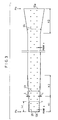
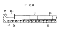
- FIG. 6 shows the floating amount of the semiconductor chip 28 transported over the transport passage 12 as the semiconductor chip 28 is moved toward the downstream side in the transport direction.
- the floating amount of the semiconductor chip 28e arrived at the terminal end Pb is at its maximum.
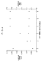
- FIG. 4 shows the difference in floating amount concerning the respective semiconductor chips 28 arranged over the transport passage 12.
- the horizontal axis indicates the serial number of the transported semiconductor chip 28 as counted from the terminal end Pb.
- the floating amount is indicated by blanked squares, and the aperture area is indicated by solid circles.
- the difference in floating amount as described above is caused as follows. That is, the larger the aperture area (clearance area) is, the larger the leakage amount of air is. Accordingly, the floating amount of the semiconductor chip 28 is decreased in such a situation. On the contrary, the smaller the aperture area (clearance area) is, the smaller the leakage amount of air is. Accordingly, the floating amount of the semiconductor chip 28 is increased in such a situation.
- the semiconductor chip 28e located at the terminal end Pb in the transport direction can be easily picked up by using an automatic transport arm without performing any manual operation.
- the automatic operation it is possible to realize the automatic operation to pick up individual objects of the large number of transported semiconductor chips 28 one by one. This results in the fully automatic operation for the entire transport system for the semiconductor chips 28.
- the transport apparatus 10 When the transport apparatus 10 according to the embodiment of the present invention is installed in a production line for the semiconductor chips 28 or in a production line for electronic apparatuses or devices, the following embodiment of use may be considered.
- the plurality of transport passages 12 provided in the main apparatus body 14 are allotted to the quality levels of the semiconductor chips 28 respectively.
- the first transport passage (transport passage located at the uppermost part in FIG. 1) 12A is allotted to transport the semiconductor chips 28 having the best quality.
- the second transport passage 12B is allotted to transport the semiconductor chips 28 having the second best quality.
- the third, fourth,... and nth transport passages 12C, 12D,... 12N are allotted to transport the semiconductor chips 28 having the third, fourth,... and nth best qualities respectively.
- the large number of semiconductor chips 28 are introduced into the corresponding transport passages 12 respectively depending on the quality level acknowledged for every one chip in the previous step, for example, in the inspection step.
- the introduction process can be performed by using, for example, a transport robot having an assigning mechanism.
- the large number of semiconductor chips 28 are assigned on the basis of the different quality levels, and they are introduced into the corresponding transport passages 12 respectively.
- the semiconductor chips 28 are transported through each of the transport passages 12 to the terminal end Pb in accordance with the air jetting and the inclination of the main apparatus body 14 while maintaining the floating state.
- Each of the semiconductor chips 28, which has arrived at the terminal end Pb in each of the transport passages 12, is floated highest owing to the relationship concerning the aperture area (or the clearance area) as described above.
- the semiconductor chips 28e floated highest over the respective transport passages 12 are picked up, for example, by the plurality of transport arms installed for each of the quality levels.
- the semiconductor chips 28e are then introduced into assembly lines for electronic apparatuses or devices installed for each of the quality levels.
- the semiconductor chips 28 are picked up by the transport arm in an order starting from a certain transport passage 12 in which a predetermined number of semiconductor chips 28 are stored.
- the semiconductor chips 28 are introduced into the assembly line for electronic apparatuses or devices.
- the semiconductor chips 28 each having substantially the same quality level can be prepared in each of the transport passages 12.
- One type of apparatuses or devices can be assembled by using the semiconductor chips 28 having substantially the same quality transported by one transport passage, for example, in the following assembling step. Thus, it is possible to improve the quality of the apparatuses or devices.
- the transport apparatus 10 makes it possible to perform the automatic operation for picking up individual semiconductor chips 28 one by one, and realize the fully automatic operation for the entire transport system for the semiconductor chips 28.
- the air-jetting holes 26, which are provided through the groove bottom surface of the transport passage 12 are disposed at the five points with respect to the projected area of the semiconductor chip 28. Accordingly, all of the large number of semiconductor chips 28, which are placed on the transport passage 12, can be floated without any fluctuation. Thus, it is possible to avoid any retention of the semiconductor chips 28 on the transport passage 12. That is, all of the large number of semiconductor chips 28 can be efficiently transported in the transport direction by means of the respective transport passages 12.
- FIGs. 7 to 12 Components or parts which are the same as those shown in FIGs. 1 to 6 are designated by the same reference numerals.
- a transport apparatus 10 according to a first modified embodiment is constructed in approximately the same manner as the transport apparatus 10 according to the embodiment of the present invention.
- the former is different from the latter in that an air blow pipe 27 is provided at the starting end Pa in the transport direction (direction indicated by the arrow in FIG. 7) of the transport passage 12, the opening of the transport surface at the terminal end Pa in the transport direction is not especially narrowed as compared with the other portions, the number of air-jetting holes 26 provided through the transport surface at the terminal end Pa is large as compared with the other portion, and a plurality of slits 29 are provided vertically through the terminal end wall 20a in the transport direction.
- the air blow pipe 27 is connected to the air supply system comprising, for example, the unillustrated air pump and the electromagnetic valve.
- the air is jetted toward the semiconductor chip 28 from a nozzle 31 disposed at the forward end of the air blow pipe 27 (air pressure: about 0.1 to 0.5 kgf/cm 2 ).
- the opening of the transport surface at the starting end Pa has a width which is wider than those of the other portions. For this reason, the phenomenon would be otherwise caused, in which the floating state of the semiconductor chip 28 is not stabilized or the semiconductor chip 28 is not floated, due to, for example, fluctuation of the pressure of air discharged from the air-jetting holes 26 provided through the transport surface.
- this phenomenon is dissolved owing to the arrangement as described above. Accordingly, it is possible to smoothly transport the semiconductor chips 28.
- the number of the air-jetting holes 26 for the transport surface at the terminal end Pb is larger than those for the other portions. Therefore, the semiconductor chip 28 can be floated highest without especially narrowing the width of the opening of the transport surface at the terminal end Pb as compared with the other portions.
- the specified number of the air-jetting holes 26 to be installed can be individually determined considering the condition concerning the semiconductor chip 28 such as the shape and the weight and the condition concerning the transport apparatus 10 such as the aperture area of the transport surface of the transport passage 12.
- the plurality of slits 29 are vertically provided through the terminal end wall 20a in the transport direction. Therefore, a part of the air for moving the semiconductor chip 28 in the transport direction or a part of the air for floating the semiconductor chip 28 leaks toward rearwardly and upwardly (in the leftward direction and in the upward direction in FIG. 7) at the terminal end wall 20 in the transport direction. Thus, the semiconductor chip 28 is smoothly moved in the transport direction, and it is possible to adjust the floating amount of the semiconductor chip 28. As described above, the phenomenon is dissolved, which would be otherwise caused such that the terminal end wall 20a in the transport direction makes a so-called drift of air.
- the transport apparatus 10 may be provided with a plurality of grooves as the transport passages 12 corresponding to the qualities of the semiconductor chips 28, wherein it is possible to adjust the transport condition for each of the transport passages 12 by changing and adjusting the condition for forming the slit 29 for each of the transport passages 12.
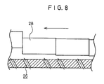
- a transport apparatus 10 according to a second modified embodiment shown in FIG. 8 is constructed in approximately the same manner as the transport apparatus 10 according to the embodiment of the present invention.
- the former is different from the latter in that the air-jetting direction of the air-jetting holes 26 provided through the transport surface is not in the upright direction, but it is inclined with respect to the transport direction (direction indicated by the arrow in FIG. 8).
- the air, which is discharged from the air-jetting holes 26, gives the semiconductor chips 28 the floating force as well as the force (thrust) for making movement in the transport direction.
- the transport apparatus 10 is allowed to have a simple structure.
- the equipment cost is reduced, and the operation is simplified.
- the simple structure makes it possible to perform the transport operation with high reliability.
- a transport apparatus 10 according to a third modified embodiment shown in FIG. 9 is constructed in approximately the same manner as the transport apparatus 10 according to the embodiment of the present invention.
- the former is different from the latter in that projections 30 are provided at the terminal end Pb of the transport passage 12.
- the two projections 30 are provided and aligned in the lateral direction respectively on the surface of the terminal end wall 20 which closes the terminal end opening 12b of each of the transport passages 12, the surface being opposed to the terminal end opening 12b.
- the semiconductor chip 28e which has arrived at the terminal end Pb, makes surface-to-surface contact with the terminal end wall 20. Therefore, in order to float the semiconductor chip 28e located at the terminal end Pb, it is necessary that the air-jetting force exerted on the semiconductor chip 28e is not less than the contact frictional force of the surface-to-surface contact. Considering the balance with respect to the floating amount of the semiconductor chip 28 which is in the transport process, it may be difficult to adjust the air-jetting amount. Further, as described above, the problem may be caused in that foreign matters would adhere to the chip 28e.
- the projections 30 are provided at the terminal end Pb. Therefore, the semiconductor chip 28e, which has arrived at the terminal end Pb, abuts against the projections 30 in point-to-point contact or in line-to-line contact therewith. Accordingly, it is possible to decrease the air-jetting force exerted on the semiconductor chip 28e. Thus, it is easy to adjust the air-jetting amount and perform other operations. Further, the adhesion of foreign matters to the semiconductor chip 28e disappears.
- a transport apparatus 10 according to a fourth modified embodiment shown in FIG. 10 is constructed in approximately the same manner as the transport apparatus 10 according to the first modified embodiment described above. However, the former is different from the latter in that projections 30 are provided at the terminal end Pb of the transport passage 12, and projections 32 are provided at the terminal end portion of the semiconductor chip 28.
- the semiconductor chip 28e which has arrived at the terminal end Pb, abuts against the following semiconductor chip 28 in line-to-line contact (or in point-to-pint contact) with the projections 32 located at the rear end thereof in the transport direction. Therefore, it is possible to further decrease the air-jetting force to be exerted on the semiconductor chip 28. It is possible to realize simplification of the control system and the structure of the air supply system.
- a transport apparatus 10 according to a fifth modified embodiment shown in FIG. 11 is constructed in approximately the same manner as the transport apparatus 10 according to the embodiment of the present invention. However, the former is different from the latter in that the semiconductor chip 28 to be introduced has a substantially trapezoidal side configuration.
- the line-to-line contact is made between the concerning semiconductor chip 28e and the terminal end wall 20 and between the concerning semiconductor chip 28e and the following semiconductor chip 28 respectively.
- the rear end of the concerning semiconductor chip 28e is moved along the tapered surface (surface inclined upwardly in the direction to make separation from the terminal end Pb) of the front end of the following semiconductor chip 28. Therefore, as the concerning semiconductor chip 28 located at the terminal end Pb is floated upwardly, the following semiconductor chip 28 is moved while making advance into the space under the concerning semiconductor chip 28e disposed at the terminal end Pb. Accordingly, the concerning semiconductor chip 28e, which is located at the terminal end Pb, is easily floated higher than the other semiconductor chips 28.
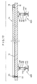
- the method for inclining the main apparatus body 14, for example, by 1° with respect to the transport direction is carried out as shown in FIG. 2 by appropriately adjusting the screwing amount of the screw 24 screwed into the main apparatus body 14 from the bottom surface side of the base pedestal 16.
- each of the lifting-rotating mechanisms 40A, 40B comprises, for example, a bolt member 44 screwed in the vertical direction into a stage 42 which is installed for a production line for producing parts or components, a support member 46 placed on a head 44a of the bolt member 44, an attachment plate 48 secured to the bottom surface of a base pedestal 16, and a support shaft 50 provided for rotatably attaching the support member 46 to the attachment plate 48.
- the screwing amount of the bolt member 44 into the stage 42 is decreased by rotating the bolt member 44 of the lifting-rotating mechanism 40A disposed on the side of the starting end opening 12a of the transport passage 12, or the screwing amount of the bolt member 44 into the stage 42 is increased by rotating the bolt member 44 of the lifting-rotating mechanism 40B disposed on the side of the terminal end opening 12b of the transport passage 12.
- the main apparatus body 14 can be easily supported, for example, at an angle of inclination of 1° with respect to the transport direction.
- the transport apparatus 10 according to the embodiment of the present invention and the transport apparatuses 10 according to the several modified embodiments have been described as exemplified by the application to the transport apparatus 10 for transporting the large number of semiconductor chips 28 in one direction.
- the transport apparatus 10 according to the present invention can be also applied to transport various types of small-sized objects.
- the object transport apparatus is provided with at least one line of groove for constructing a transport passage for an object, wherein the transport passage comprises a mechanism for moving the object in a transport direction, a floating mechanism for the object, and a floating-accelerating mechanism for the object disposed at a terminal end in the transport direction.
- the transport system is realized in which the object is transported in one direction while floating the object by means of air. Especially, it is possible to realize the automatic operation for picking up individual objects one by one.
Landscapes
- Engineering & Computer Science (AREA)
- Manufacturing & Machinery (AREA)
- Microelectronics & Electronic Packaging (AREA)
- Container, Conveyance, Adherence, Positioning, Of Wafer (AREA)
Claims (12)
- Objekt-Transportvorrichtung, die mit zumindest einer Rillenreihe versehen ist, um einen Transportweg (12) zum Transportieren eines Gegenstands (28) zu konstruieren, wobei die Objekt-Transportvorrichtung umfasst:einen Mechanismus (24, 31, 40A, 40B), um den Gegenstand in einer Transportrichtung zu bewegen; undeinen Schwebemechanismus (26), wobei die Objekt-Transportvorrichtung dadurch gekennzeichnet ist, dass sie einen Schwebe-Beschleunigungsmechanismus umfasst, der an einem Abschlussende (20) in der Transportrichtung angeordnet ist.
- Objekt-Transportvorrichtung nach Anspruch 1, worin der Mechanismus zum Bewegen des Gegenstands in der Transportrichtung zumindest eines aus einem Mittel (24, 40A, 40B) zum Neigen des Transportwegs nach unten in einem vorbestimmten Winkel zur Transportrichtung, eine große Anzahl an Luftstrahllöchern (26), die durch eine Transportfläche des Transportwegs hindurch ausgebildet sind, so dass Luft in der Transportrichtung ausgestoßen wird, und einem Schiebemittel (27, 31) umfasst, das in die Transportrichtung gerichtet an einem Anfangsende (Pa) des Transportwegs in der Transportrichtung vorgesehen ist.
- Objekt-Transportvorrichtung nach Anspruch 1, worin der Schwebemechanismus eine große Anzahl an Luftstrahllöchern (26) aufweist, die durch eine Objekt-Transportfläche des Transportwegs (12) hindurch ausgebildet sind.
- Objekt-Transportvorrichtung nach Anspruch 1, worin der Schwebe-Beschleunigungsmechanismus zumindest eines aus einem Mittel, mit dem eine planare Konfiguration des Transportwegs eine solche Gestalt aufweisen kann, dass ein Schwebeausmaß des Gegenstands am Abschlussende in Transportrichtung maximiert wird, und einem Mittel mit einer großen Anzahl an Luftstrahllöchern (26) umfasst, die durch eine Objekt-Transportfläche des Transportwegs ausgebildet sind, um eine Luftausstoßmenge von Luftstrahllöchern der großen Anzahl an Luftstrahllöchern, die am Abschlussende in der Transportrichtung angeordnet sind, im Vergleich zu einer Luftstrahlmenge der Luftstrahllöcher zu erhöhen, die an anderen Positionen als dem Abschlussende in Transportrichtung angeordnet sind.
- Objekt-Transportvorrichtung nach einem der Ansprüche 1 bis 4, worin die Rillen zum Bilden der Objekt-Transportwege (12) parallel zueinander in einer Anzahl von Reihen vorgesehen sind, die Qualitätsniveaus der Objekte entsprechen.
- Objekt-Transportvorrichtung nach einem der Ansprüche 1 bis 5, worin die Luftstrahllöcher (26) an drei Punkten oder mehr in Bezug auf eine projizierte Fläche des Objekts vorgesehen sind.
- Objekt-Transportvorrichtung nach einem der Ansprüche 1 bis 6, worin der Transportweg (12) eine planare Konfiguration aufweist, bei der eine Freifläche in der Transportrichtung schrittweise verringert ist, mit der Maßgabe, dass es sich bei der Freifläche um eine Fläche handelt, die durch Subtrahieren der projizierten Fläche des Objekts von einer Fläche einer Objekt-Transportfläche des Transportwegs handelt.
- Objekt-Transportvorrichtung nach einem der Ansprüche 1 bis 7, worin ein Schlitz (29) in der Transportrichtung durch eine Abschlussendwand (20a) des Transportwegs (12) hindurch vorgesehen ist.
- Objekt-Transportvorrichtung nach einem der Ansprüche 1 bis 8, worin ein Vorsprung (30) auf einer Abschlussendwand (20) des Transportwegs (12) in der Transportrichtung vorgesehen ist.
- Objekt-Transportvorrichtung nach Anspruch 9, worin ein Vorsprung (32) an einem hinteren Ende des Objekts (28) in der Transportrichtung vorgesehen ist.
- Objekt-Transportvorrichtung nach einem der Ansprüche 1 bis 9, worin das Objekt ein Elektronikteil ist.
- Objekt-Transportvorrichtung nach Anspruch 11, worin eine Länge des Objekts entlang der Transportrichtung in einer Richtung seiner Höhe kontinuierlich abnimmt.
Applications Claiming Priority (7)
| Application Number | Priority Date | Filing Date | Title |
|---|---|---|---|
| JP318797 | 1997-01-10 | ||
| JP3187/97 | 1997-01-10 | ||
| JP318797 | 1997-01-10 | ||
| JP346840/97 | 1997-12-16 | ||
| JP34684097 | 1997-12-16 | ||
| JP34684097A JP3581000B2 (ja) | 1997-01-10 | 1997-12-16 | 物品搬送装置 |
| PCT/JP1998/000066 WO1998030480A1 (en) | 1997-01-10 | 1998-01-09 | Article conveyor |
Publications (3)
| Publication Number | Publication Date |
|---|---|
| EP0905064A1 EP0905064A1 (de) | 1999-03-31 |
| EP0905064A4 EP0905064A4 (de) | 2000-04-05 |
| EP0905064B1 true EP0905064B1 (de) | 2003-04-16 |
Family
ID=26336713
Family Applications (1)
| Application Number | Title | Priority Date | Filing Date |
|---|---|---|---|
| EP98900208A Expired - Lifetime EP0905064B1 (de) | 1997-01-10 | 1998-01-09 | Förderer für gegenstände |
Country Status (5)
| Country | Link |
|---|---|
| US (1) | US6224298B1 (de) |
| EP (1) | EP0905064B1 (de) |
| JP (1) | JP3581000B2 (de) |
| DE (1) | DE69813433T2 (de) |
| WO (1) | WO1998030480A1 (de) |
Families Citing this family (9)
| Publication number | Priority date | Publication date | Assignee | Title |
|---|---|---|---|---|
| NL1015030C2 (nl) * | 2000-04-14 | 2001-10-16 | Fico Bv | Werkwijze en inrichting voor transport van elektronische componenten. |
| US6606739B2 (en) * | 2000-11-14 | 2003-08-12 | Ball Semiconductor, Inc. | Scaling method for a digital photolithography system |
| DE10157703B4 (de) * | 2001-11-24 | 2004-05-06 | Weidenmüller, Ralf | Vorrichtung zum gleichzeitigen Fördern und Temperieren von Formteilen |
| AU2003223905A1 (en) * | 2003-04-03 | 2004-11-01 | Braun Gmbh | Device for producing a predetermined orientation |
| WO2006064562A1 (ja) * | 2004-12-16 | 2006-06-22 | Ueno Seiki Co., Ltd. | パーツフィーダ |
| JP2007238193A (ja) * | 2006-03-06 | 2007-09-20 | Kanto Auto Works Ltd | 物品の搬送装置 |
| JP2011178560A (ja) * | 2010-02-04 | 2011-09-15 | Eiko Sangyo Kk | チップ部品の整列供給装置 |
| JP2014080291A (ja) * | 2012-09-28 | 2014-05-08 | Toray Precision Kk | 浮上搬送装置及び浮上搬送方法 |
| CN108408412B (zh) * | 2018-01-31 | 2019-07-05 | 河海大学 | 用于粉体材料输运的主动搓板式流化床管道及其使用方法 |
Family Cites Families (9)
| Publication number | Priority date | Publication date | Assignee | Title |
|---|---|---|---|---|
| US3731823A (en) * | 1971-06-01 | 1973-05-08 | Ibm | Wafer transport system |
| US4730955A (en) * | 1986-05-13 | 1988-03-15 | Precision Metal Fabricators, Inc. | Divergent single filer |
| IT1235967B (it) * | 1989-12-22 | 1992-12-09 | Gd Spa | Apparecchiatura per l'alimentazione di prodotti, per esempio cioccolatini,ad una unita'operatrice |
| JPH0574684A (ja) | 1991-09-13 | 1993-03-26 | Nikon Corp | 位置合わせ装置 |
| JPH069052A (ja) * | 1991-12-25 | 1994-01-18 | Nifco Inc | ワークの搬送装置 |
| JPH0574684U (ja) * | 1992-03-13 | 1993-10-12 | 三共精工株式会社 | 被搬送物の判別振分装置 |
| JPH0780011A (ja) * | 1993-09-14 | 1995-03-28 | Menicon Co Ltd | 眼用レンズ製作用材の搬送装置および搬送方法 |
| JPH0891623A (ja) * | 1994-09-28 | 1996-04-09 | Fujitsu Ltd | 基板搬送方法及び基板搬送装置 |
| US5634636A (en) * | 1996-01-11 | 1997-06-03 | Xerox Corporation | Flexible object handling system using feedback controlled air jets |
-
1997
- 1997-12-16 JP JP34684097A patent/JP3581000B2/ja not_active Expired - Fee Related
-
1998
- 1998-01-09 WO PCT/JP1998/000066 patent/WO1998030480A1/ja not_active Ceased
- 1998-01-09 US US09/142,329 patent/US6224298B1/en not_active Expired - Lifetime
- 1998-01-09 DE DE69813433T patent/DE69813433T2/de not_active Expired - Lifetime
- 1998-01-09 EP EP98900208A patent/EP0905064B1/de not_active Expired - Lifetime
Also Published As
| Publication number | Publication date |
|---|---|
| JPH10250841A (ja) | 1998-09-22 |
| JP3581000B2 (ja) | 2004-10-27 |
| DE69813433D1 (de) | 2003-05-22 |
| WO1998030480A1 (en) | 1998-07-16 |
| US6224298B1 (en) | 2001-05-01 |
| EP0905064A1 (de) | 1999-03-31 |
| DE69813433T2 (de) | 2004-03-04 |
| EP0905064A4 (de) | 2000-04-05 |
Similar Documents
| Publication | Publication Date | Title |
|---|---|---|
| EP0905064B1 (de) | Förderer für gegenstände | |
| KR100849003B1 (ko) | 칩 부품 반송 방법 및 장치, 및 외관 검사 방법 및 장치 | |
| US7296344B2 (en) | Apparatus for mounting component | |
| JP4440219B2 (ja) | 担持体上に半導体デバイスを位置合わせするための装置及び方法 | |
| JP4814833B2 (ja) | ボウル型パーツフィーダ | |
| EP2437290A1 (de) | Werkstücktransportverfahren und Werkstücktransportvorrichtung | |
| US20080069677A1 (en) | Transport object levitation unit, transport object levitation apparatus and stage apparatus | |
| JP2006191121A5 (de) | ||
| KR102475997B1 (ko) | 기판 상에 솔더 볼들을 배치하기 위한 조립체 및 방법 | |
| JPWO2005049287A1 (ja) | 真空吸着ヘッド、その真空吸着ヘッドを用いた真空吸着装置及びテーブル | |
| JP2018064048A (ja) | レーザ照射装置、レーザ照射方法、及び半導体装置の製造方法 | |
| KR19990013707A (ko) | 마이크로 볼 그리드 어레이용 에어-블로우 솔더 볼 로딩 시스템 | |
| KR20200001966A (ko) | 얼라인먼트 장치, 반도체 웨이퍼 처리장치 및 얼라인먼트 방법 | |
| US20070267463A1 (en) | Apparatus for mounting columns for grid array electronic packages | |
| US6592729B2 (en) | In-line sputtering apparatus | |
| US20220033208A1 (en) | Transport device | |
| CN119069398A (zh) | 晶圆传输装置及半导体工艺设备 | |
| US6573520B1 (en) | Electron beam lithography system | |
| KR20140029694A (ko) | 부상방식의 기판 이송 장치의 높이 조절 장치 및 방법, 및 이를 구비한 부상방식의 기판 이송 장치 및 코팅 장치 | |
| US20020124964A1 (en) | Wafer support plate assembly having recessed upper pad and vacuum processing apparatus comprising the same | |
| US6371310B1 (en) | Boat for land grid array packages | |
| JP2018114476A (ja) | 塗布装置および塗布方法 | |
| WO2024185424A1 (ja) | 基板保持装置 | |
| JP2025117028A (ja) | 実装装置及び実装装置の制御方法 | |
| KR20260040762A (ko) | 반송 및 정렬 장치 |
Legal Events
| Date | Code | Title | Description |
|---|---|---|---|
| PUAI | Public reference made under article 153(3) epc to a published international application that has entered the european phase |
Free format text: ORIGINAL CODE: 0009012 |
|
| 17P | Request for examination filed |
Effective date: 19980930 |
|
| AK | Designated contracting states |
Kind code of ref document: A1 Designated state(s): DE FR GB |
|
| A4 | Supplementary search report drawn up and despatched |
Effective date: 20000221 |
|
| AK | Designated contracting states |
Kind code of ref document: A4 Designated state(s): DE FR GB |
|
| GRAG | Despatch of communication of intention to grant |
Free format text: ORIGINAL CODE: EPIDOS AGRA |
|
| 17Q | First examination report despatched |
Effective date: 20020426 |
|
| GRAG | Despatch of communication of intention to grant |
Free format text: ORIGINAL CODE: EPIDOS AGRA |
|
| GRAG | Despatch of communication of intention to grant |
Free format text: ORIGINAL CODE: EPIDOS AGRA |
|
| GRAH | Despatch of communication of intention to grant a patent |
Free format text: ORIGINAL CODE: EPIDOS IGRA |
|
| GRAH | Despatch of communication of intention to grant a patent |
Free format text: ORIGINAL CODE: EPIDOS IGRA |
|
| GRAA | (expected) grant |
Free format text: ORIGINAL CODE: 0009210 |
|
| AK | Designated contracting states |
Designated state(s): DE FR GB |
|
| REG | Reference to a national code |
Ref country code: GB Ref legal event code: FG4D |
|
| REF | Corresponds to: |
Ref document number: 69813433 Country of ref document: DE Date of ref document: 20030522 Kind code of ref document: P |
|
| ET | Fr: translation filed | ||
| PLBE | No opposition filed within time limit |
Free format text: ORIGINAL CODE: 0009261 |
|
| STAA | Information on the status of an ep patent application or granted ep patent |
Free format text: STATUS: NO OPPOSITION FILED WITHIN TIME LIMIT |
|
| 26N | No opposition filed |
Effective date: 20040119 |
|
| PGFP | Annual fee paid to national office [announced via postgrant information from national office to epo] |
Ref country code: GB Payment date: 20121228 Year of fee payment: 16 |
|
| PGFP | Annual fee paid to national office [announced via postgrant information from national office to epo] |
Ref country code: DE Payment date: 20130131 Year of fee payment: 16 Ref country code: FR Payment date: 20130128 Year of fee payment: 16 |
|
| REG | Reference to a national code |
Ref country code: DE Ref legal event code: R119 Ref document number: 69813433 Country of ref document: DE |
|
| GBPC | Gb: european patent ceased through non-payment of renewal fee |
Effective date: 20140109 |
|
| REG | Reference to a national code |
Ref country code: DE Ref legal event code: R119 Ref document number: 69813433 Country of ref document: DE Effective date: 20140801 |
|
| PG25 | Lapsed in a contracting state [announced via postgrant information from national office to epo] |
Ref country code: DE Free format text: LAPSE BECAUSE OF NON-PAYMENT OF DUE FEES Effective date: 20140801 |
|
| REG | Reference to a national code |
Ref country code: FR Ref legal event code: ST Effective date: 20140930 |
|
| PG25 | Lapsed in a contracting state [announced via postgrant information from national office to epo] |
Ref country code: FR Free format text: LAPSE BECAUSE OF NON-PAYMENT OF DUE FEES Effective date: 20140131 Ref country code: GB Free format text: LAPSE BECAUSE OF NON-PAYMENT OF DUE FEES Effective date: 20140109 |