EP0907085A1 - Verfahren zum Messen von Wiederstandsänderungen durch Elektromigration - Google Patents
Verfahren zum Messen von Wiederstandsänderungen durch Elektromigration Download PDFInfo
- Publication number
- EP0907085A1 EP0907085A1 EP97870149A EP97870149A EP0907085A1 EP 0907085 A1 EP0907085 A1 EP 0907085A1 EP 97870149 A EP97870149 A EP 97870149A EP 97870149 A EP97870149 A EP 97870149A EP 0907085 A1 EP0907085 A1 EP 0907085A1
- Authority
- EP
- European Patent Office
- Prior art keywords
- current
- mosfet
- conductive pattern
- same
- conductive
- Prior art date
- Legal status (The legal status is an assumption and is not a legal conclusion. Google has not performed a legal analysis and makes no representation as to the accuracy of the status listed.)
- Withdrawn
Links
- 238000000034 method Methods 0.000 title claims abstract description 37
- 239000000758 substrate Substances 0.000 claims abstract description 14
- 229910052802 copper Inorganic materials 0.000 claims description 5
- 239000000463 material Substances 0.000 claims description 5
- 229910052782 aluminium Inorganic materials 0.000 claims description 3
- 229910052737 gold Inorganic materials 0.000 claims description 2
- 229910000838 Al alloy Inorganic materials 0.000 claims 1
- RYGMFSIKBFXOCR-UHFFFAOYSA-N Copper Chemical compound [Cu] RYGMFSIKBFXOCR-UHFFFAOYSA-N 0.000 claims 1
- 229910000881 Cu alloy Inorganic materials 0.000 claims 1
- 239000004411 aluminium Substances 0.000 claims 1
- XAGFODPZIPBFFR-UHFFFAOYSA-N aluminium Chemical compound [Al] XAGFODPZIPBFFR-UHFFFAOYSA-N 0.000 claims 1
- 239000010949 copper Substances 0.000 claims 1
- PCHJSUWPFVWCPO-UHFFFAOYSA-N gold Chemical compound [Au] PCHJSUWPFVWCPO-UHFFFAOYSA-N 0.000 claims 1
- 239000010931 gold Substances 0.000 claims 1
- 239000011810 insulating material Substances 0.000 claims 1
- 239000004065 semiconductor Substances 0.000 claims 1
- 238000012360 testing method Methods 0.000 abstract description 76
- 238000005259 measurement Methods 0.000 abstract description 40
- 230000002708 enhancing effect Effects 0.000 abstract 1
- 230000035882 stress Effects 0.000 description 24
- 238000010438 heat treatment Methods 0.000 description 6
- 238000011161 development Methods 0.000 description 4
- 230000018109 developmental process Effects 0.000 description 4
- 239000002184 metal Substances 0.000 description 4
- 229910052751 metal Inorganic materials 0.000 description 4
- 230000001939 inductive effect Effects 0.000 description 3
- 238000005184 irreversible process Methods 0.000 description 3
- 238000004519 manufacturing process Methods 0.000 description 3
- 230000002441 reversible effect Effects 0.000 description 3
- VYPSYNLAJGMNEJ-UHFFFAOYSA-N Silicium dioxide Chemical compound O=[Si]=O VYPSYNLAJGMNEJ-UHFFFAOYSA-N 0.000 description 2
- ATJFFYVFTNAWJD-UHFFFAOYSA-N Tin Chemical compound [Sn] ATJFFYVFTNAWJD-UHFFFAOYSA-N 0.000 description 2
- 239000000956 alloy Substances 0.000 description 2
- 229910045601 alloy Inorganic materials 0.000 description 2
- 230000004888 barrier function Effects 0.000 description 2
- 239000004020 conductor Substances 0.000 description 2
- 238000000691 measurement method Methods 0.000 description 2
- XUIMIQQOPSSXEZ-UHFFFAOYSA-N Silicon Chemical compound [Si] XUIMIQQOPSSXEZ-UHFFFAOYSA-N 0.000 description 1
- 230000032683 aging Effects 0.000 description 1
- 239000000919 ceramic Substances 0.000 description 1
- 229910052681 coesite Inorganic materials 0.000 description 1
- 230000001276 controlling effect Effects 0.000 description 1
- 238000012937 correction Methods 0.000 description 1
- 230000002596 correlated effect Effects 0.000 description 1
- 229910052906 cristobalite Inorganic materials 0.000 description 1
- 238000013461 design Methods 0.000 description 1
- 238000010586 diagram Methods 0.000 description 1
- 230000000694 effects Effects 0.000 description 1
- 230000008030 elimination Effects 0.000 description 1
- 238000003379 elimination reaction Methods 0.000 description 1
- 238000002474 experimental method Methods 0.000 description 1
- 238000001556 precipitation Methods 0.000 description 1
- 230000000630 rising effect Effects 0.000 description 1
- 229910052710 silicon Inorganic materials 0.000 description 1
- 239000010703 silicon Substances 0.000 description 1
- 239000000377 silicon dioxide Substances 0.000 description 1
- 229910052682 stishovite Inorganic materials 0.000 description 1
- 229910052905 tridymite Inorganic materials 0.000 description 1
Images


Classifications
-
- G—PHYSICS
- G01—MEASURING; TESTING
- G01R—MEASURING ELECTRIC VARIABLES; MEASURING MAGNETIC VARIABLES
- G01R31/00—Arrangements for testing electric properties; Arrangements for locating electric faults; Arrangements for electrical testing characterised by what is being tested not provided for elsewhere
- G01R31/28—Testing of electronic circuits, e.g. by signal tracer
- G01R31/2851—Testing of integrated circuits [IC]
- G01R31/2855—Environmental, reliability or burn-in testing
- G01R31/2856—Internal circuit aspects, e.g. built-in test features; Test chips; Measuring material aspects, e.g. electro migration [EM]
- G01R31/2858—Measuring of material aspects, e.g. electro-migration [EM], hot carrier injection
Definitions
- the present invention is related to a method for evaluating electromigration induced early resistance changes in conductive materials, particularly in interconnect patterns as currently present on integrated circuits. Testing for electromigration during the development and manufacture of integrated circuits is indispensable to ensure a qualified performance during lifetime.
- the reliability of integrated circuits and particularly of the interconnect patterns being part of these integrated circuits is an important topic in the development, the fabrication and the use of integrated circuits.
- the effect of these disturbances on the lifetime of conductive patterns strongly depends on several parameters like e.g. the dimensions of those patterns, the current density and the conductive material used: e.g. Al, Cu or an alloy thereof.
- Conventional examples of criteria to identify failure in a current driven conductive pattern during lifetime, the so-called high value failure criteria are a line opening in said conductive pattern or a 10% resistance change.
- several conductive test structures were produced in order to determine these failures. The test times needed to meet these conventional failure criteria are far too extensive and therefore these criteria are inadequate especially in the development phase of an IC process where a rapid performance feedback is indispensable.
- ERC early resistance change
- This absolute measurement technique is addressed by e.g. the European patent EP 0395149 A1.
- This test technique measures the resistance, i.e. the resistance changes, of a conductive pattern during a limited period in an environment with a high temperature stability in a very accurate way.
- the intrinsic resistance of the conductive pattern is measured.
- a high current density is applied to the conductive pattern in order to enhance electromigration and a plurality of resistance measurements is performed while the test time elapses in order to determine the resistance changes.
- the major disadvantage of this technique is that one can not distinguish between the different disturbances inducing failure, i.e. it is not possible to distinguish between electromigration and resistance changes induced by temperature changes, i.e. due to power dissipation which can be quite significant at large current densities.
- test and reference two identical structures, i.e. two conductive patterns having the same dimensions and the same resistance, hereafter called test and reference which are processed on the same substrate in close vicinity of each other.
- test and reference One reason to implement two different structures can be to correct the measurements on the test structure for the external thermal induced resistance changes.
- the test structure is then stressed at a high current density, while the reference structure is sensing only a very small measuring current.
- the measurement on this reference structure is used to correct the measurement on the test structure for the external thermal induced resistance changes (see e.g. A Scorzoni et al, Materials Science Reports 7, p. 143-220, 1991).
- Another reason to implement two structures as in the United States patent US 5264377, can be to correct for the topographic influences but in the latter case the structures are not identical.
- the power dissipation in the test structure can be quite substantial because the test structure is sensing a high current density, while the power dissipation in the reference structure is much lower than in the test structure due to a huge difference in current density level. Furthermore because test and reference structure are so close to each other the large temperature increase in the test structure due to the power dissipation will affect the temperature of the reference structure. Consequently, it is still not possible to separate electromigration induced failures from failures induced by other disturbances. These disturbances are mainly thermal processes initiated by thermal changes caused by the power dissipation. Examples of such processes are Joule heating and the reversible and irreversible processes induced in a conductive pattern by Joule heating like e.g. precipitation.
- a method of measuring early resistance changes is disclosed to study electromigration induced failures in conductive patterns.
- Said method can provide a basis for lifetime predictions based on low value failure criteria, i.e. small resistance changes in said conductive patterns in a limited period of time.
- Two identical so-called test and reference structures are placed close to each other on the same substrate and submitted to at least one sequence of a stress period and a measurement period.
- Said identical test and reference structures are in fact two conductive patterns having the same dimensions, the same layout and the same intrinsic resistance.
- Said structures are composed of the same materials, are at about the same temperature and are processed on the same substrate in vicinity of each other.
- a DC high density stress current which enhances electromigration
- a symmetric pulsed AC current which has no influence on electromigration
- the amplitude of the AC current is chosen such that both the DC current and the AC current result in the same power dissipation in both structures during said stress period.
- the latter can be achieved by applying currents having the same root mean square (rms) value. Consequently the temperature changes in the reference structure and in the test structure are identical.
- two identical AC currents i.e. having the same amplitude and frequency, are applied to the reference and test structure respectively.
- a method allowing to determine resistance changes induced by electromigration.
- the currents applied to both the test structure and the reference structure during the stress period(s) as well as during the measurement period(s) are generated by one and the same source. Therefore, drift of said source is also excluded because the resistance changes induced by this drift are identical in both the test structure and the reference structure.
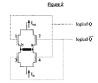
- MOSFET switches are implemented to realise this.
- Such a MOSFET switch as in fig. 2, comprises four identical MOSFET's, which can be all n-channel devices as well as p-channel devices.
- the drains of MOSFET 3 and 4 are connected to the sources of MOSFET's 1 and 2 respectively.
- the connection from the drain of MOSFET 3 to the drain of MOSFET 4 comprises either one of a test structure or a reference structure.
- the MOSFET's 2 and 3 are in ON-state while the MOSFET's 1 and 4 are in the OFF-state, which can be accomplished by using an invertor. In the latter case, the current is flowing in the opposite direction (from b to a) through either one of a test or reference structure.
- a single current meter can be applied thereby also excluding the influence of drift of the current meter on the measurement results.
- a method for determining resistance changes induced by electromigration in a conductive pattern comprising at least one sequence of the steps of:
- a method of measuring early resistance changes is disclosed to study non-electrical induced failures in conductive patterns.
- Said method can provide a basis for lifetime predictions based on low value failure criteria, i.e. small resistance changes in said conductive patterns in a limited period of time.
- the method of the present invention allows one to distinguish in a very accurate way between electromigration induced failures and failures induced by other disturbances like temperature changes due to Joule heating, external temperature fluctuations, reversible and irreversible processes induced in the conductive patterns by Joule heating.
- test and reference structures are placed close to each other and submitted to at least one sequence of a stress period and a measurement period.
- Said essentially identical test and reference structures are in fact two conductive patterns having substantially the same characteristics, like e.g. the same dimensions, the same layout and the same intrinsic resistance.
- Said structures are composed of the same materials, are at about the same temperature and are placed on the same substrate in close vicinity of each other.
- a DC high density stress current is applied to the test structure, while simultaneously a symmetric pulsed AC current, typically with a frequency between 100 Hz and 10 kHz, is applied to the reference structure.
- the amplitude of the AC current is chosen such that the dissipated power in both the test and reference structure is the same. The latter can be achieved by choosing the same rms value for the DC and the AC current. Consequently the temperature changes in the test and reference structure are identical for both structures.
- the DC current is a uni-directional current and because the DC current density is chosen high enough to guarantee accelerated ageing, electromigration is enhanced in the test structure and thus also the resistance changes induced by electromigration.
- the applied DC current density is typically about 1 MA per cm 2 or higher.
- the bi-directional symmetric AC current in the reference structure does not introduce electromigration.
- each measurement cycle within a measurement period comprises in practice a sequence of four resistance measurements: T+, R+, R-, T- as illustrated in fig.1.
- the resistance of both the reference structure (R+, R-) and the test structure (T+, T-) is measured twice.
- the latter is performed in order to enhance the accuracy of the determination of the resistance changes induced by disturbances.
- the only difference between the test structure and the reference is the difference in resistance induced by electromigration which is introduced in the test structure during the stress period. All other disturbances inducing resistance changes are corrected for by subtracting the resistance value of the reference structure from the resistance value of the test structure as determined during the measurement period.
- a method is disclosed allowing to distinguish in a very accurate way between electromigration induced failures and failures induced by other disturbances like temperature changes due to Joule heating, external temperature fluctuations, reversible and irreversible processes induced in the conductive patterns by Joule heating. Furthermore the currents applied to both the test structure and the reference structure during the stress period(s) as well as during the measurement period(s) are generated by one and the same source. Therefore, drift of said source is also excluded because the resistance changes induced by this drift are identical in both the test structure and the reference structure.
- MOSFET switches are implemented to achieve this.
- Such a MOSFET switch as in fig.2, comprises four identical MOSFET's, which can be all n-channel devices as well as p-channel devices. Said MOSFET's have the same dimensions and are characterised by the same electrical parameters.
- the drains of MOSFET 3 and 4 are connected to the sources of MOSFET's 1 and 2 respectively.
- the connection from the drain of MOSFET 3 to the drain of MOSFET 4 comprises either one of a test structure or a reference structure.
- the resistance can be determined by measuring the output current and the voltage drop between (a) and (b).
- the MOSFET's 2 and 3 are in the ON-state while the MOSFET's 1 and 4 are in the OFF-state, which can be accomplished by using an invertor. In the latter case, the current is flowing in the opposite direction (from b to a) through either on of the test or reference structure.
- the current flows through MOSFET 4, via the test structure (from a to b) and leaves the switch through MOSFET 1 as the uni-directional output current I test .
- the control signal level is kept high during the whole stress period.
- This DC current I test is fed in to a second MOSFET switch, comprising four identical MOSFET's and a reference structure, which is connected in series with said first MOSFET switch.
- the MOSFET's 5 and 8 are in the ON-state, while MOSFET 6 and 7 are in OFF-state, which can be accomplished by inverting the control signal.
- the current flows through MOSFET 8, via the reference structure (from (c) to (d)) and leaves the switch through MOSFET 5 as the output current I out .
- the MOSFET's 6 and 7 are in the ON-state while the MOSFET's 5 and 8 are in the OFF-state, which can be accomplished by using an invertor.
- the current is flowing in the opposite direction (from (d) to (c)) through the reference structure. By doing so a symmetric alternating current is generated in the reference structure.
- the frequency of this current is correlated to the switching speed of the MOSFET switch, i.e. the frequency of the binary control signal.
- the same MOSFET switches can be used in an analogous way, i.e. by applying multiple control signals, to provide two identical AC currents during a measurement period. Said AC currents having the same amplitude as the currents during the stress period.
- the resistance values of the test structure and the reference structure can be determined by measuring the current and the voltage drop over the test structure (between (a) and (b)) and the reference structure (between (c) and (d)).
- test and reference structures are submitted to at least one sequence of a stress period and a measurement period.
- Said identical test and reference structures are in fact two conductive patterns having the same dimensions, the same layout and the same intrinsic resistance.
- Said structures are composed of the same materials and are processed on the same substrate.
- said conductive patterns can be metal stripes or metal multi-finger structures.
- said conductive patterns can comprise a single conductive layer or multiple conductive layers.
- Said conductive layer can be a metal like Al, Cu, Au or an alloy thereof.
- Said conductive layers can be passivated or not.
- the two conductive patterns are two non-passivated metal patterns comprising four layers: a first Al layer, with 1 weight percentage (wt%) Si and 0.5 wt% Cu, a Ti barrier layer , Ti and TiN ARC layers. These patterns are processed on the same substrate, i.e. a silicon substrate covered with SiO 2 . These patterns each have the same dimensions. Their length is 2 mm, the width is 10 micrometer, the thickness of the AlSiCu layer, the Ti barrier layer, the Ti ARC layer and the TiN Arc layer are respectively 4400, 500, 200 and 600 Angstrom.
- the sequence of stress and measurement periods is performed at an external ambient temperature of 220 deg °C.
- a DC current with a current density of 3 MA/cm 2 is applied to the test structure, while an AC current is applied to the reference structure.
- Said AC current, having a frequency of 100 Hz is chosen such that the dissipated power in the reference structure is the same as the dissipated power in the test structure.
- both the test and reference structure are sensing the same current, having a period of 80 ms. The power dissipation associated with each of these currents is the same as during the stress period.
- the equipment used for performing the measurements of resistance changes is: a multimeter (Keithley 2001) for measuring the current and the voltage drop over either one of a test or a reference structure, an in-house built current source, control circuitry e.g. for controlling the MOSFET switches, a furnace (own design gas-flow type furnace with a temperature stability of about 0.01 °C).
- the test and reference structure were processed on the same substrate at a distance of 500 micrometer from each other. A part of said substrate, comprising both the test and the reference structure was mounted in a DIL24 ceramic package.
- the measurement resolution of the non-corrected signals measured on the test and reference structure being in fact the measurement resolution of an absolute measurement, is about 400 ppm, while the measurement resolution of the corrected, i.e.
- the resistance changes of the test and reference structure show the same non-linear increase of about 3000 ppm; the resistance changes of the reference structure then saturate towards the end of the measurement sequence.
- the resistance changes of the test structure initially follow the behaviour of the resistance changes of the reference structure but then start to decrease before rising quasi-linearly.
- the corrected resistance changes are only those induced by electromigration: after applying the stress current the corrected resistance changes almost immediately start to decrease before increasing monotonically.
Landscapes
- Engineering & Computer Science (AREA)
- Environmental & Geological Engineering (AREA)
- Computer Hardware Design (AREA)
- Microelectronics & Electronic Packaging (AREA)
- General Engineering & Computer Science (AREA)
- Physics & Mathematics (AREA)
- General Physics & Mathematics (AREA)
- Testing Or Measuring Of Semiconductors Or The Like (AREA)
Priority Applications (2)
| Application Number | Priority Date | Filing Date | Title |
|---|---|---|---|
| EP97870149A EP0907085A1 (de) | 1997-10-03 | 1997-10-03 | Verfahren zum Messen von Wiederstandsänderungen durch Elektromigration |
| US09/165,486 US6136619A (en) | 1997-10-03 | 1998-10-02 | Method for measuring electromigration-induced resistance changes |
Applications Claiming Priority (1)
| Application Number | Priority Date | Filing Date | Title |
|---|---|---|---|
| EP97870149A EP0907085A1 (de) | 1997-10-03 | 1997-10-03 | Verfahren zum Messen von Wiederstandsänderungen durch Elektromigration |
Publications (1)
| Publication Number | Publication Date |
|---|---|
| EP0907085A1 true EP0907085A1 (de) | 1999-04-07 |
Family
ID=8231046
Family Applications (1)
| Application Number | Title | Priority Date | Filing Date |
|---|---|---|---|
| EP97870149A Withdrawn EP0907085A1 (de) | 1997-10-03 | 1997-10-03 | Verfahren zum Messen von Wiederstandsänderungen durch Elektromigration |
Country Status (2)
| Country | Link |
|---|---|
| US (1) | US6136619A (de) |
| EP (1) | EP0907085A1 (de) |
Cited By (3)
| Publication number | Priority date | Publication date | Assignee | Title |
|---|---|---|---|---|
| WO2003076954A3 (en) * | 2002-03-08 | 2003-12-31 | Univ Brown Res Found | High resolution scanning magnetic microscope operable at high temperature |
| SG127775A1 (en) * | 2001-11-30 | 2006-12-29 | Tokyo Electron Ltd | Reliability evaluation test apparatus, reliabilityevaluation test system, contactor, and reliabilit y evaluation test method |
| EP2264445B1 (de) * | 2009-06-15 | 2017-01-25 | Deutsches Zentrum für Luft- und Raumfahrt e. V. | Coulometrischer Feuchtesensor und entsprechendes Verfahren |
Families Citing this family (12)
| Publication number | Priority date | Publication date | Assignee | Title |
|---|---|---|---|---|
| US6350626B1 (en) * | 1999-10-01 | 2002-02-26 | United Microelectronics Corp. | Method of testing electromigration lifetime |
| US6466038B1 (en) * | 2000-11-30 | 2002-10-15 | Lsi Logic Corporation | Non-isothermal electromigration testing of microelectronic packaging interconnects |
| TWI221908B (en) * | 2002-06-25 | 2004-10-11 | Infineon Technologies Ag | Electromigration test apparatus and an electromigration test method |
| US6724214B2 (en) * | 2002-09-13 | 2004-04-20 | Chartered Semiconductor Manufacturing Ltd. | Test structures for on-chip real-time reliability testing |
| US7146588B1 (en) * | 2004-08-02 | 2006-12-05 | Advanced Micro Devices, Inc. | Predicting EM reliability by decoupling extrinsic and intrinsic sigma |
| US20060066335A1 (en) * | 2004-09-28 | 2006-03-30 | Kang Seung H | Semiconductor test device with heating circuit |
| US7355201B2 (en) * | 2006-06-27 | 2008-04-08 | Advanced Micro Devices, Inc. | Test structure for measuring electrical and dimensional characteristics |
| US20080036487A1 (en) * | 2006-08-09 | 2008-02-14 | Arm Limited | Integrated circuit wearout detection |
| GB2440764B (en) * | 2006-08-09 | 2011-03-02 | Advanced Risc Mach Ltd | Integrated circuit wearout detection |
| US8410560B2 (en) * | 2010-01-21 | 2013-04-02 | Cambridge Cmos Sensors Ltd. | Electromigration reduction in micro-hotplates |
| US8917104B2 (en) | 2011-08-31 | 2014-12-23 | International Business Machines Corporation | Analyzing EM performance during IC manufacturing |
| US8890556B2 (en) | 2011-10-26 | 2014-11-18 | International Business Machines Corporation | Real-time on-chip EM performance monitoring |
Citations (3)
| Publication number | Priority date | Publication date | Assignee | Title |
|---|---|---|---|---|
| EP0395149A1 (de) * | 1989-04-19 | 1990-10-31 | Interuniversitair Microelektronica Centrum Vzw | Verfahren und Anordnung zur beschleunigten Bestimmung der Alterung von einem oder mehreren Elementen mit einem elektromagnetischen Alterungsparameter |
| JPH0377080A (ja) * | 1989-08-18 | 1991-04-02 | Nippon Telegr & Teleph Corp <Ntt> | 配線層のエレクトロマイグレーション寿命測定法及びそれに用いる装置 |
| EP0656650A1 (de) * | 1993-06-21 | 1995-06-07 | OHMI, Tadahiro | Stromgesteuerte auswertungsmethode von leitenden materialien |
Family Cites Families (3)
| Publication number | Priority date | Publication date | Assignee | Title |
|---|---|---|---|---|
| US5264377A (en) * | 1990-03-21 | 1993-11-23 | At&T Bell Laboratories | Integrated circuit electromigration monitor |
| US5497076A (en) * | 1993-10-25 | 1996-03-05 | Lsi Logic Corporation | Determination of failure criteria based upon grain boundary electromigration in metal alloy films |
| JP3077080B2 (ja) | 1994-06-30 | 2000-08-14 | 関東自動車工業株式会社 | メータの取り付け構造 |
-
1997
- 1997-10-03 EP EP97870149A patent/EP0907085A1/de not_active Withdrawn
-
1998
- 1998-10-02 US US09/165,486 patent/US6136619A/en not_active Expired - Fee Related
Patent Citations (3)
| Publication number | Priority date | Publication date | Assignee | Title |
|---|---|---|---|---|
| EP0395149A1 (de) * | 1989-04-19 | 1990-10-31 | Interuniversitair Microelektronica Centrum Vzw | Verfahren und Anordnung zur beschleunigten Bestimmung der Alterung von einem oder mehreren Elementen mit einem elektromagnetischen Alterungsparameter |
| JPH0377080A (ja) * | 1989-08-18 | 1991-04-02 | Nippon Telegr & Teleph Corp <Ntt> | 配線層のエレクトロマイグレーション寿命測定法及びそれに用いる装置 |
| EP0656650A1 (de) * | 1993-06-21 | 1995-06-07 | OHMI, Tadahiro | Stromgesteuerte auswertungsmethode von leitenden materialien |
Non-Patent Citations (2)
| Title |
|---|
| PATENT ABSTRACTS OF JAPAN vol. 15, no. 245 (P - 1218) 24 June 1991 (1991-06-24) * |
| SCORZONI A ET AL: "Electromigration in thin-film interconnection lines: models, methods and results", MATERIAL SCIENCE REPORTS, DEC. 1991, NETHERLANDS, vol. 7, no. 4-5, ISSN 0920-2307, pages 143 - 220, XP002057760 * |
Cited By (6)
| Publication number | Priority date | Publication date | Assignee | Title |
|---|---|---|---|---|
| SG127775A1 (en) * | 2001-11-30 | 2006-12-29 | Tokyo Electron Ltd | Reliability evaluation test apparatus, reliabilityevaluation test system, contactor, and reliabilit y evaluation test method |
| US7242206B2 (en) | 2001-11-30 | 2007-07-10 | Tokyo Electron Limited | Reliability evaluation test apparatus, reliability evaluation test system, contactor, and reliability evaluation test method |
| US8456186B2 (en) * | 2001-11-30 | 2013-06-04 | Tokyo Electron Limited | Reliability evaluation test apparatus, reliability evaluation test system, contactor, and reliability evaluation test method |
| WO2003076954A3 (en) * | 2002-03-08 | 2003-12-31 | Univ Brown Res Found | High resolution scanning magnetic microscope operable at high temperature |
| US6930479B2 (en) | 2002-03-08 | 2005-08-16 | Brown University Research Foundation | High resolution scanning magnetic microscope operable at high temperature |
| EP2264445B1 (de) * | 2009-06-15 | 2017-01-25 | Deutsches Zentrum für Luft- und Raumfahrt e. V. | Coulometrischer Feuchtesensor und entsprechendes Verfahren |
Also Published As
| Publication number | Publication date |
|---|---|
| US6136619A (en) | 2000-10-24 |
Similar Documents
| Publication | Publication Date | Title |
|---|---|---|
| US6136619A (en) | Method for measuring electromigration-induced resistance changes | |
| US5264377A (en) | Integrated circuit electromigration monitor | |
| US7471101B2 (en) | Systems and methods for controlling of electro-migration | |
| US5420513A (en) | Dielectric breakdown prediction and dielectric breakdown life-time prediction using iterative voltage step stressing | |
| Salmen et al. | A new test procedure to realistically estimate end-of-life electrical parameter stability of SiC MOSFETs in switching operation | |
| Schreiber | Electromigration threshold in aluminum films | |
| US4795964A (en) | Method and apparatus for measuring the capacitance of complementary field-effect transistor devices | |
| JP4982190B2 (ja) | 電子電力回路における電流温度測定方法、および、電流温度測定装置 | |
| US6320391B1 (en) | Interconnection device for low and high current stress electromigration and correlation study | |
| US8754655B2 (en) | Test structure, method and circuit for simultaneously testing time dependent dielectric breakdown and electromigration or stress migration | |
| CN100412561C (zh) | 电致迁移测试装置及电致迁移测试方法 | |
| CN1502132A (zh) | 测定绕线可靠性之电子迁移测试结构 | |
| Snyder et al. | Novel self-stressing test structures for realistic high-frequency reliability characterization | |
| EP0448273B1 (de) | Elektromigrationsüberwachungseinrichtung für integrierte Schaltungen | |
| US6897476B1 (en) | Test structure for determining electromigration and interlayer dielectric failure | |
| Jeckelmann et al. | Optimization of QHE-devices for metrological applications | |
| Overney et al. | Longitudinal impedance measurements on graphene QHE devices | |
| CN110146800B (zh) | 一种igct器件的门极电流及关断特性测量方法 | |
| Pham et al. | Influence of metallization layout on aging detector lifetime under cyclic thermo-mechanical stress | |
| KR101003870B1 (ko) | 일렉트로마이그레이션 측정을 위한 장치 및 방법 | |
| JPH06201761A (ja) | 絶縁膜の経時絶縁破壊特性測定方法 | |
| Sajadi et al. | Gate Oxide and Package Reliability of TO-263 SiC MOSFETs | |
| JP2003083871A (ja) | 電子部品の接合部の信頼性試験方法 | |
| JP2007165365A (ja) | 半導体装置及びそのテスト方法 | |
| JP2000243800A (ja) | 配線のエレクトロマイグレーション耐性評価方法 |
Legal Events
| Date | Code | Title | Description |
|---|---|---|---|
| PUAI | Public reference made under article 153(3) epc to a published international application that has entered the european phase |
Free format text: ORIGINAL CODE: 0009012 |
|
| 17P | Request for examination filed |
Effective date: 19971022 |
|
| AK | Designated contracting states |
Kind code of ref document: A1 Designated state(s): AT BE CH DE ES FR GB IE IT LI NL SE |
|
| AX | Request for extension of the european patent |
Free format text: AL;LT;LV;RO;SI |
|
| AKX | Designation fees paid |
Free format text: AT BE CH DE ES FR GB IE IT LI NL SE |
|
| STAA | Information on the status of an ep patent application or granted ep patent |
Free format text: STATUS: THE APPLICATION IS DEEMED TO BE WITHDRAWN |
|
| 18D | Application deemed to be withdrawn |
Effective date: 20050503 |