EP0656650A1 - Stromgesteuerte auswertungsmethode von leitenden materialien - Google Patents
Stromgesteuerte auswertungsmethode von leitenden materialien Download PDFInfo
- Publication number
- EP0656650A1 EP0656650A1 EP94918543A EP94918543A EP0656650A1 EP 0656650 A1 EP0656650 A1 EP 0656650A1 EP 94918543 A EP94918543 A EP 94918543A EP 94918543 A EP94918543 A EP 94918543A EP 0656650 A1 EP0656650 A1 EP 0656650A1
- Authority
- EP
- European Patent Office
- Prior art keywords
- current
- wiring
- flowing
- migration
- wiring pattern
- Prior art date
- Legal status (The legal status is an assumption and is not a legal conclusion. Google has not performed a legal analysis and makes no representation as to the accuracy of the status listed.)
- Withdrawn
Links
Images



Classifications
-
- G—PHYSICS
- G01—MEASURING; TESTING
- G01R—MEASURING ELECTRIC VARIABLES; MEASURING MAGNETIC VARIABLES
- G01R31/00—Arrangements for testing electric properties; Arrangements for locating electric faults; Arrangements for electrical testing characterised by what is being tested not provided for elsewhere
- G01R31/28—Testing of electronic circuits, e.g. by signal tracer
- G01R31/2851—Testing of integrated circuits [IC]
- G01R31/2855—Environmental, reliability or burn-in testing
- G01R31/2856—Internal circuit aspects, e.g. built-in test features; Test chips; Measuring material aspects, e.g. electro migration [EM]
- G01R31/2858—Measuring of material aspects, e.g. electro-migration [EM], hot carrier injection
-
- G—PHYSICS
- G01—MEASURING; TESTING
- G01R—MEASURING ELECTRIC VARIABLES; MEASURING MAGNETIC VARIABLES
- G01R27/00—Arrangements for measuring resistance, reactance, impedance, or electric characteristics derived therefrom
- G01R27/02—Measuring real or complex resistance, reactance, impedance, or other two-pole characteristics derived therefrom, e.g. time constant
-
- G—PHYSICS
- G01—MEASURING; TESTING
- G01R—MEASURING ELECTRIC VARIABLES; MEASURING MAGNETIC VARIABLES
- G01R31/00—Arrangements for testing electric properties; Arrangements for locating electric faults; Arrangements for electrical testing characterised by what is being tested not provided for elsewhere
- G01R31/28—Testing of electronic circuits, e.g. by signal tracer
- G01R31/2801—Testing of printed circuits, backplanes, motherboards, hybrid circuits or carriers for multichip packages [MCP]
- G01R31/281—Specific types of tests or tests for a specific type of fault, e.g. thermal mapping, shorts testing
- G01R31/2812—Checking for open circuits or shorts, e.g. solder bridges; Testing conductivity, resistivity or impedance
Definitions
- the present invention relates to a method of evaluating current-driven conductive material, and more particularly to a method of evaluating electro-migration resistance and stress migration resistance of various types of current-driven conductive material independently and efficiently.
- wiring material for LSI As wiring material for LSI, at present, such materials as Al, Al-Si alloy prepared by mixing several percents of Si in Al or Ai-Si-Cu alloy in which a small quantity of Cu is mixed have been used.
- the present inventor succeeded in shortening a time required for a reliability test for wiring, without causing melting of wiring, by repeating the operational sequence comprising the steps of flowing a first current in a wiring pattern, then measuring a resistance value of the wiring, then flowing a second current having a larger current value than the first current to heat this wiring, simultaneously controlling temperature of the wiring pattern by means of cooling it from the outside to prevent the wiring temperature from becoming uncontrollable, turning off the second current, and then again flowing the first current (Japanese Patent Application No.126732/1991).
- Japanese Patent Application No.126732/1991 Japanese Patent Application No.126732/1991
- the present invention was made in the light of the circumstances as described above, and it is an object of the present invention to provide a method of evaluating current-driven conductive material which enables independent evaluation of a capability of wiring material to withstand electro-migration and stress migration within a short period of time and also enables feedback of test data effective for development of wiring material.
- a first gist of of the present invention consists in a method of evaluating current-driven conductive material characterized in that, in a method of evaluating within a shorter period of time a capability of the wiring pattern to withstand electro-migration by repeating several times an operating sequence comprising the steps of flowing a first current in a wiring pattern made of conductive material, then measuring a resistance value of the wiring, then flowing a second current having a larger current value than the first current to generate electro-migration in the wiring pattern, turning off the second current, and then again flowing the first current, a capability of the wiring pattern to withstand electro-migration is measured by controlling temperature rise while the second current is flowing at a level by 50°C lower or more than the temperature while the first current is flowing by means of setting a time for flowing the second current fully shorter than the time for flowing the first current.
- a second gist of of the present invention consists in a method of evaluating current-driven conductive material characterized in that, in a method of evaluating within a shorter period of time a capability of the wiring pattern to withstand stress migration by repeating several times an operating sequence comprising the steps of flowing a first current in a wiring pattern made of conductive material, then measuring a resistance value of the wiring, then flowing a second current having a larger current value than the first current to generate stress migration in the wiring pattern, turning off the second current, and then again flowing the first current, stress migration generated in the wiring pattern is measured by setting the second current to a current value at which practically electro-migration does not occur, setting a repeat cycle of flowing the second current to 10 msec or less, and also setting a time for flowing the second current so that temperature of the wiring pattern while the second current is flowing will be 100°C or more higher than temperature whole the first current is flowing.
- a resistance value is monitorred by flowing a first current having a current density not generating electro-migration, electro-migration is generated by flowing a second current having a high current density, and a capability of wiring to withstand electro-migration is measured regarding the time required until the resistance value drops to a specified value as a life of the wiring.
- this step by setting a time and a cycle for flowing the second current so that temperature due to Joule's heat generated when the second current is loaded to wiring will not rise to 50°C or more higher than temperature of the wiring generated when the first current is flow, it is possible to prevent acceleration of electro-migration caused by temperature rise due to uncontrolable heat dissipation which can hardly be controlled and also to measure electro-migration at a specified temperature. Also as temperature rise in the wiring is held under 50°C, practically stress migration does not occur, and as a result it is possible to accurately estimate only the wiring 's capability to withstand electro-migration under any conditions using the Black's empirical expression (Expression (1)).
- Fig.1 shows a device used for evaluation of a capability of wiring to withstand electro-migration as well as a capability thereof to withstand stress migration.
- designated at the reference numeral 1 is a substrate on which wiring made of conductive material is formed, at 2 a printed board having a pin for connection with outside, at 3 a substrate holding means, at 4 a vessel for heated fluid, at 5 a heated fluid inlet port, at 6 a heated fluid discharge port, at 7 a heated fluid inlet pipe, at 8 a partition, at 9 a flow rate control means, at 10 a flow meter, at 11 a heated fluid temperature control means, and at 12 piping.
- a typical example of conductive material is, for instance, material for LSI.
- Material for LSI includes, for instance, Al, Al-Si (2 to 5 %) alloy, Al-Si (1 to 5 %(-Cu (1 to 5 %) alloy, Cu, W,Mo, Ti, WSi2, MoSi2, TiSi2, or polysilicon, and wiring in which these materials are deposited in a layered form, such as wiring in which, for instance, high melting point materials are overlaid alternatively.
- superconductive material is one of the conductive materials.
- a substrate for instance, Si wafer, a substrate with a 0.01 to 1 ⁇ m silicon oxide film or a silicon nitride film formed thereon, a glass substrate, a ceramic substrate made of such a material as alumina, a copper substrate with an insulating film made of such as material as SiO2 formed thereon are available.
- the thermal conductivity is high and accordingly the cooling efficiency becomes higher, and for this reason it is possible to carry out an experiment at a higher current density.
- a thin film made of wiring material is formed by means of, for instance, deposition, sputtering, CVD, or MOCVD method with a thickness from 0.7 to 1 ⁇ m, and a wiring pattern for measuring a capability of the wiring to withstand electro-migration or stress migration with a length in a range from 0.1 to 1 mm and a width in a range from 0.3 to 5 ⁇ m is formed.
- a means for holding a substrate (substrate holding means) anything is allowable on the condition that it can hold a substrate with a wiring pattern formed thereon and can be fitted to a temperature control means, but a copper plate, an aluminium plate or a ceramic plate having a diameter larger than that of a substrate and a thickness from 2 to 5 mm is preferable. Of these, a copper plate having a high thermal conductivity is especially preferable.
- a substrate may be adhered to the substrate holding means using, for instance, low melting point metal such as indium.
- a plurality of substrates may be held by a substrate holding means.
- a printed board for drawing for connecting a wiring pattern to a power supply unit or a measurement instrument may be held by the substrate holding means.
- a means for flowing a first current in wiring comprises a connecting means, such as, for instance, wire bonding, for connecting a pad section of a wiring pattern to a corresponding pad of a printed board, a connecting means, such as, for instance, a connector, for connecting a drawing pin of the printed board to a power supply unit, and a power supply unit.
- a connecting means such as, for instance, wire bonding
- a connecting means such as, for instance, a connector
- a means for measuring a resistance value of wiring comprises a connecting means such as , for instance, wire bonding for connecting a pad section of a wiring pattern to a corresponding pad of a printed board, a connecting means such as, for instance, a connector for connecting a pin of the printed board to a voltmeter, and a voltmeter.
- a means for flowing a first current may be shared, or it may be provided separately.
- power supply is not limited to DC power supply, and AD power supply may be used.
- the AD power supply may be either one having a sinosoidal wave output or one having a pulse output. It is needless to say that DC current with AD current superimposed thereon may be used.
- AD power supply it is preferable to use AD power supply, and it is especially preferable to use AD power supply having the same absolute value. With this means, electro-migration can be suppressed furthermore, and it is possible to measure stress migration under a high current density and high temperature.
- the heated fluid inlet port 5 is connected to the heated fluid inlet pipe 7 inside the vessel 1, and heat generated in the wiring is efficiently removed or heat is supplied to the wiring, so that a tip of the inlet pipe is located just under the substrate 1.
- the partition 8 surrounding the inlet pipe 7 is provided to prevent air from residing therein.
- the discharge port 6 is fitted to a position lower than an upper edge of the partition and is communicated to an inlet port of the heated fluid temperature control means through a heat-insulating pipe 12.
- the heated fluid inlet port 5 is connected via the flow meter 10, flow rate control means 9, and heat-insulating pipe 12 to the heated fluid temperature control means 11.
- the heated fluid flow rate control means 9 and the heated fluid temperature control 11 are provided to control a flow rate and a temperature of heated fluid according to an input signal provided from the wiring temperature detecting means and to maintain temperature of the wiring at a specified value.
- thermometer such as a thermocouple or a non-contact type of thermometer such as a collector element or a thermopile may be used.
- Wiring temperature is maintained at a specified value by controlling a flow rate and a temperature of a heated fluid.
- a means for controlling a flow rate of a heated fluid a general valve may be used, but an electro-magnetic valve, which can control a flow rate of a heated fluid according to an output signal from the temperature detecting means described above, is preferable.
- a means for controlling temperature of a heated fluid for instance, a thermostatic bath is used, but a thermostatic bath having a heater and a cooler for controlling a temperature of a heated fluid according to an output signal from the temperature detecting means like in case of the flow rate control means is preferable.
- Fig.2(a) shows change in a resistance value of a wiring pattern when a first current and a second current are flown repeatedly.
- a current not causing electro-migration for instance, a current with a current density in a range from 102 to 106 A/cm2 is flowing in a conductive wiring pattern and an initial resistance value of the wiring is obtained from a voltage difference between two edges of the wiring. Then a second current having a pulse width so small that temperature rise due to Joule's heat dissipation can not follow is loaded.
- This pulse width is decided from a relation between this pulse width and a current density to be used, and in case of a current density in range from 106 to 109 A/cm2, a pulse width in a range from 10 psec to around 50 nsec is used. Also a duty ratio of less than 50 % is usually used.
- the wiring temperature then is set by only a substrate temperature control means. Intensity of a second current then is defined with an output current value of a pulse. For this reason intensity and a testing temperature of a current causing electro-migration can be controlled separately. For measuring different temperatures, a temperature of a heated fluid may be changed. On the other hand, temperature rise due to a second current can be suppressed to below 50°C, so that stress migration can practically be ignored.
- a resistance value is again measured.
- the resistance value then becomes larger than the initial value because of the electro-migration effect caused by a second current loaded thereto.
- the cycle above is repeated, the resistance value becomes gradually larger, the time required until the resistance value becomes by 5 % or 10 % larger than the initial value is regarded as a life of the wiring. This life may be defined depending on any period of time required for any degree of change in a resistance value on the wiring. Measurement of the resistance value when a first current is flown may be carried out after a second current pulse is loaded several times repeatedly.
- the first current may be either DC current or AD current.
- AD current electro-migration effect generated when the resistance value is measured is suppressed.
- unknown constants A and E are decided by carrying out the above testing under two or more different temperatures.
- a product of a life by a current density can be obtained for electro-migration under any temperature, and for instance, it is possible to estimates a life under a certain current density or a maximum allowable current density to a required life.
- Fig.2B shows change in a resistance value of a wiring pattern when a first current and a second current are flown repeatedly.
- a first current with a current density in a range from 102 to 104 A/cm2 is flown in a conductive wiring pattern, and an initial resistance value of wiring is obtained from a voltage difference between both edges of the pattern.
- a second current is loaded using a pulse current with a current density, at which the electro-migration effect is small, for instance in a range from 104 to 106 A/cm2 and yet at which dissipation of Joule's heat occurs adequately.
- the wiring temperature then is decided not only by the substrate temperature control means, but also by Joule's heat generated in the wiring.
- Intensity of the second current is defined with an output current value of the pulse.
- a resistance value is again measured.
- the resistance value then becomes larger than the initial value because of the stress migration effect caused by a second current loaded thereto.
- the cycle above is repeated, the resistance value becomes gradually larger, the time required until the resistance value becomes by 5 % or 10 % larger than the initial value is regarded as a life of the wiring. This life may be defined depending on any period of time required for any degree of change in a resistance value on the wiring. Measurement of the resistance value when a first current is flown may be carried out after a second current is loaded several times repeatedly.
- the first and second currents may be either DC current or AD current.
- heat is generated when a second current is flown, but as a current is loaded in a form of pulses, the effect by stress generated by dissipation of Joule's heat becomes larger, and it becomes possible to obtain change of a resistance value due to only stress migration within a shorter period of time. Also as unnecessary heat generated when a second current is flown to heat wiring can effectively be removed by the substrate temperature control means, and as a result uncontrollable temperature rise can be suppressed. Namely by flowing a current having a longer pulse width, it becomes possible to carry out the withstand stress migration evaluation test under a higher temperature.
- a cu film having a thickness of 1 ⁇ m was formed by means of deposition or sputtering on an Si wafer with a 5 ⁇ m thermally oxidized film on a surface thereof. Then by etching, 100 pieces of 1 mm x 1 mm VANDER PAUW pattern were formed on a substrate. A silicon oxide film having a thickness of 1 ⁇ m was formed on a surface of the wafer by means of CVD method, and the pad section was removed by etching, and then a substrate was formed by dicing.
- This substrate and a ceramic printed board having a pad for wire bonding as well as a pin for drawing to outside were adhered to a 50 mm ⁇ and 2 mmt copper plate using indium, and then wiring on the substrate and the corresponding pad on the printed board were connected to each other by means of wire bonding.
- This copper plate was fixed through an O ring to the vessel shown in Fig.1 with screws.
- the heated fluid inlet port and a discharge port of the vessel were connected to a thermostatic bath, and the heated fluid was always maintained at a specified temperature.
- a pulse power supply source and an oscilloscope 1 are connected in series to one of the two sets of pad, and an oscilloscope 2 was connected to a pad 2 in the other set.
- signal inlet/outlet ports of the pulse power source and oscilloscopes 1,2 are connected to a computer, and a value of a first current, a value of a second current, on/off timing, a resistance value of wiring, temperature of the wiring, and temperature of heated fluid were computed and controlled by the computer. Then a life of the wiring against electro-migration was obtained in the following way.
- a first current was flown in each wiring, and a resistance value of each wiring was measured. Then, the current value was transitionally risen to a second current value corresponding to a specified current density, the second current was maintained for a short period of time so that the temperature would not rise, and then the current value was transitionally dropped to the first current value, thus a resistance value being measured. The above operating sequence was repeated until the resistance value rose by 5 % from the initial value.
- the first current and the second current had a current density of 1 x 10⁴ A/cm2 and 0.5 to 1.5 x 10⁷ A/cm2, a pulse width of 10 nsec, and a duty ratio of 0.5 respectively.
- the temperature of the heated fluid was set to 77 °C and 127 °C respectively.
- the wiring temperature when the current temperature was flown was obtained from a resistance value when the second current was flown, but temperature rise was not observed in any case of current density in a range from 0.5 to 5 x 10⁷ A/cm2.
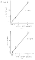
- Fig.4 (a), (b) The life time until a resistance value of the wiring rose by 5 % is shown in Fig.4 (a), (b).
- the straight lines in the figures were obtained by subjecting average values of data at each temperature to linear approximation by means of method of least square. Slopes of straight lines in Fig.4 (a), (b) coincided with each other. Namely, the expression (1) was satisfied, indicating that E and A can accurately be measured by carrying out measurement changing a temperature. In this embodiment, E was 1.2, while A was 3. In the conventional type of measurement, E is o.8 and A is 2.65, indicating that, according to this embodiment, effect by stress migration can be eliminated and deterioration of wiring due to only electro-migration can be achieved.
- each resistance value was measured. Then the current value was transitionally raised to a second current value corresponding to a specified current density to raise the temperature, and then the current value was transitionally dropped to the first current value, and the resistance value was measured.
- the first and second currents had a current density of 1 x 10² A/cm2 and 4 x 10⁴A/cm2, the second current had a pulse width of 100 nsec and 10 ⁇ sec, and a duty ratio of 0.5, and a temperature of the heated fluid was set to 127°C. Temperature of the wiring when the second current was flown rose by 100°C for a pulse width of 100 nsec or by 210°C for a pulse width of 10 ⁇ sec as compared to the temperature when the first current was flown.
Landscapes
- Engineering & Computer Science (AREA)
- Physics & Mathematics (AREA)
- General Physics & Mathematics (AREA)
- Environmental & Geological Engineering (AREA)
- Computer Hardware Design (AREA)
- Microelectronics & Electronic Packaging (AREA)
- General Engineering & Computer Science (AREA)
- Testing Or Measuring Of Semiconductors Or The Like (AREA)
- Internal Circuitry In Semiconductor Integrated Circuit Devices (AREA)
- Testing Of Individual Semiconductor Devices (AREA)
- Investigating Or Analyzing Materials By The Use Of Electric Means (AREA)
Applications Claiming Priority (3)
| Application Number | Priority Date | Filing Date | Title |
|---|---|---|---|
| JP14883193A JP3611338B2 (ja) | 1993-06-21 | 1993-06-21 | 電流駆動導電性材料評価方法 |
| JP148831/93 | 1993-06-21 | ||
| PCT/JP1994/000991 WO1995000971A1 (en) | 1993-06-21 | 1994-06-21 | Method of evaluating current-driven conductive material |
Publications (2)
| Publication Number | Publication Date |
|---|---|
| EP0656650A1 true EP0656650A1 (de) | 1995-06-07 |
| EP0656650A4 EP0656650A4 (de) | 1997-02-26 |
Family
ID=15461710
Family Applications (1)
| Application Number | Title | Priority Date | Filing Date |
|---|---|---|---|
| EP94918543A Withdrawn EP0656650A4 (de) | 1993-06-21 | 1994-06-21 | Stromgesteuerte auswertungsmethode von leitenden materialien. |
Country Status (4)
| Country | Link |
|---|---|
| US (1) | US5554938A (de) |
| EP (1) | EP0656650A4 (de) |
| JP (1) | JP3611338B2 (de) |
| WO (1) | WO1995000971A1 (de) |
Cited By (4)
| Publication number | Priority date | Publication date | Assignee | Title |
|---|---|---|---|---|
| EP0907085A1 (de) * | 1997-10-03 | 1999-04-07 | Interuniversitair Microelektronica Centrum Vzw | Verfahren zum Messen von Wiederstandsänderungen durch Elektromigration |
| WO2004031792A1 (en) * | 2002-09-30 | 2004-04-15 | Advanced Micro Devices, Inc. | Method and system for establishing a relation between joule heating and a current density in a conductor |
| WO2004048985A1 (de) * | 2002-11-23 | 2004-06-10 | Infineon Technologies Ag | Vorrichtung und verfahren zur erfassung von stressmigrations-eigenschaften |
| US7888672B2 (en) | 2002-11-23 | 2011-02-15 | Infineon Technologies Ag | Device for detecting stress migration properties |
Families Citing this family (7)
| Publication number | Priority date | Publication date | Assignee | Title |
|---|---|---|---|---|
| DE69608359T2 (de) | 1995-02-01 | 2001-02-08 | Asahi Kasei Kogyo K.K., Osaka | Hexaazaisowurtzitan-derivate und verfahren zu deren herstellung |
| DE10108915A1 (de) * | 2001-02-23 | 2002-09-12 | Infineon Technologies Ag | Elektromigrations-Teststruktur zur Erfassung einer Zuverlässigkeit von Verdrahtungen |
| US6835578B1 (en) * | 2003-09-26 | 2004-12-28 | Taiwan Semiconductor Manufacturing Company, Ltd. | Test structure for differentiating the line and via contribution in stress migration |
| CN102384930B (zh) * | 2010-09-03 | 2013-10-30 | 中国石油化工股份有限公司 | 变压器油抗氧化性能的评价方法 |
| US10591531B2 (en) * | 2015-06-10 | 2020-03-17 | Qualcomm Incorporated | Method and apparatus for integrated circuit monitoring and prevention of electromigration failure |
| EP3492935B1 (de) * | 2017-12-01 | 2021-08-11 | Mitsubishi Electric R&D Centre Europe B.V. | Gesundheitsüberwachung eines leistungshalbleiterbauelements |
| JP7126681B2 (ja) * | 2018-05-08 | 2022-08-29 | 国立大学法人東海国立大学機構 | 金属膜の製造方法 |
Family Cites Families (7)
| Publication number | Priority date | Publication date | Assignee | Title |
|---|---|---|---|---|
| USRE32625E (en) * | 1983-01-05 | 1988-03-15 | Syracuse University | Dynamic testing of electrical conductors |
| JPH01500784A (ja) * | 1986-09-17 | 1989-03-16 | ザ ゼネラル エレクトリック カンパニー,ピー.エル.シー. | 集積回路の製造方法 |
| JPH0727948B2 (ja) * | 1989-08-18 | 1995-03-29 | 日本電信電話株式会社 | 配線層のエレクトロマイグレーション寿命測定法及びそれに用いる装置 |
| SG30537G (en) * | 1990-03-21 | 1995-09-01 | At & T Corp | Integrated circuit electromigration monitor |
| JPH04186745A (ja) * | 1990-11-21 | 1992-07-03 | Hitachi Ltd | パルスエレクトロマイグレーション評価法 |
| JPH04329654A (ja) * | 1991-04-30 | 1992-11-18 | Tadahiro Omi | 電流駆動導電性材料評価方法および装置 |
| US5291142A (en) * | 1992-05-08 | 1994-03-01 | Tadahiro Ohmi | Method and apparatus for measuring the resistance of conductive materials due to electromigration |
-
1993
- 1993-06-21 JP JP14883193A patent/JP3611338B2/ja not_active Expired - Fee Related
-
1994
- 1994-06-21 EP EP94918543A patent/EP0656650A4/de not_active Withdrawn
- 1994-06-21 WO PCT/JP1994/000991 patent/WO1995000971A1/ja not_active Ceased
- 1994-06-21 US US08/387,920 patent/US5554938A/en not_active Expired - Lifetime
Cited By (9)
| Publication number | Priority date | Publication date | Assignee | Title |
|---|---|---|---|---|
| EP0907085A1 (de) * | 1997-10-03 | 1999-04-07 | Interuniversitair Microelektronica Centrum Vzw | Verfahren zum Messen von Wiederstandsänderungen durch Elektromigration |
| US6136619A (en) * | 1997-10-03 | 2000-10-24 | Interuniversitair Micorelektronica Centrum (Imec, Vzw) | Method for measuring electromigration-induced resistance changes |
| WO2004031792A1 (en) * | 2002-09-30 | 2004-04-15 | Advanced Micro Devices, Inc. | Method and system for establishing a relation between joule heating and a current density in a conductor |
| US6770847B2 (en) | 2002-09-30 | 2004-08-03 | Advanced Micro Devices, Inc. | Method and system for Joule heating characterization |
| WO2004048985A1 (de) * | 2002-11-23 | 2004-06-10 | Infineon Technologies Ag | Vorrichtung und verfahren zur erfassung von stressmigrations-eigenschaften |
| CN100554988C (zh) * | 2002-11-23 | 2009-10-28 | 因芬尼昂技术股份公司 | 检测应力迁移性质的装置及方法 |
| US7888672B2 (en) | 2002-11-23 | 2011-02-15 | Infineon Technologies Ag | Device for detecting stress migration properties |
| DE10254756B4 (de) * | 2002-11-23 | 2011-07-07 | Infineon Technologies AG, 81669 | Vorrichtung und Verfahren zur Erfassung von Stressmigrations-Eigenschaften |
| US8323991B2 (en) | 2002-11-23 | 2012-12-04 | Infineon Technologies Ag | Method for detecting stress migration properties |
Also Published As
| Publication number | Publication date |
|---|---|
| JPH0714897A (ja) | 1995-01-17 |
| EP0656650A4 (de) | 1997-02-26 |
| US5554938A (en) | 1996-09-10 |
| WO1995000971A1 (en) | 1995-01-05 |
| JP3611338B2 (ja) | 2005-01-19 |
Similar Documents
| Publication | Publication Date | Title |
|---|---|---|
| US5291142A (en) | Method and apparatus for measuring the resistance of conductive materials due to electromigration | |
| EP0656650A1 (de) | Stromgesteuerte auswertungsmethode von leitenden materialien | |
| De Moor et al. | Fabrication and reliability testing of Ti/TiN heaters | |
| EP0283778A1 (de) | Verfahren zur thermischen Charakterisierung des Gehäuses von Halbleiterbaueinheiten | |
| Rzepka et al. | Characterization of self-heating in advanced VLSI interconnect lines based on thermal finite element simulation | |
| US5260668A (en) | Semiconductor surface resistivity probe with semiconductor temperature control | |
| Griffin Jr et al. | The effective transverse thermal conductivity of amorphous Si3N4 thin films | |
| Schafft et al. | The measurement, use and interpretation of the temperature coefficient of resistance of metallizations | |
| Taylor et al. | The specific heats and resistivities of molybdenum, tantalum, and rhenium | |
| US20030029232A1 (en) | Coupon for measuring corrosion rates and system | |
| Wang et al. | In situ integration of high-temperature thin-film sensor for precise measurement of heat flux and temperature on superalloy substrate | |
| Hong et al. | Breakdown energy of metal (BEM)-A new technique for monitoring metallization reliability at wafer level | |
| US5225663A (en) | Heat process device | |
| Gwinn et al. | Apparatus for accurate measurement of interface resistance of high performance thermal interface materials | |
| Fantini et al. | Electromigration testing of integrated circuit interconnections | |
| US5281025A (en) | Temperature sensing device for dynamically measuring temperature fluctuation in a tip of a bonding device | |
| Schafft et al. | Electromigration and the current density dependence | |
| US6784000B2 (en) | Method for measurement of electromigration in semiconductor integrated circuits | |
| US6819124B1 (en) | Detection of electromigration in integrated circuits | |
| JP3468300B2 (ja) | 薄膜熱電物質の熱的及び電気的特性を測定する方法及び装置 | |
| JP2002016117A (ja) | 半導体ウェハの処理温度測定方法及び温度測定手段を備える半導体ウェハ | |
| JPH04329654A (ja) | 電流駆動導電性材料評価方法および装置 | |
| Gierczak et al. | Design, fabrication and experimental characterization of mixed thick-/thin film thermoelectric microgenerators based on constantan/silver | |
| RU2170992C2 (ru) | Микронагреватель | |
| Wieczorek et al. | Thermal conductivity of amorphous films |
Legal Events
| Date | Code | Title | Description |
|---|---|---|---|
| PUAI | Public reference made under article 153(3) epc to a published international application that has entered the european phase |
Free format text: ORIGINAL CODE: 0009012 |
|
| 17P | Request for examination filed |
Effective date: 19950308 |
|
| AK | Designated contracting states |
Kind code of ref document: A1 Designated state(s): DE GB NL |
|
| A4 | Supplementary search report drawn up and despatched |
Effective date: 19961114 |
|
| AK | Designated contracting states |
Kind code of ref document: A4 Designated state(s): DE GB NL |
|
| 17Q | First examination report despatched |
Effective date: 19970605 |
|
| STAA | Information on the status of an ep patent application or granted ep patent |
Free format text: STATUS: THE APPLICATION IS DEEMED TO BE WITHDRAWN |
|
| 18D | Application deemed to be withdrawn |
Effective date: 19971013 |