EP0910120A2 - Herstellungsverfahren für einen Bismuth enthaltenden dünnen ferroelektrischen Film - Google Patents
Herstellungsverfahren für einen Bismuth enthaltenden dünnen ferroelektrischen Film Download PDFInfo
- Publication number
- EP0910120A2 EP0910120A2 EP98119403A EP98119403A EP0910120A2 EP 0910120 A2 EP0910120 A2 EP 0910120A2 EP 98119403 A EP98119403 A EP 98119403A EP 98119403 A EP98119403 A EP 98119403A EP 0910120 A2 EP0910120 A2 EP 0910120A2
- Authority
- EP
- European Patent Office
- Prior art keywords
- thin film
- layer
- structured ferroelectric
- buffer layer
- layer structured
- Prior art date
- Legal status (The legal status is an assumption and is not a legal conclusion. Google has not performed a legal analysis and makes no representation as to the accuracy of the status listed.)
- Withdrawn
Links
Images


Classifications
-
- H—ELECTRICITY
- H10—SEMICONDUCTOR DEVICES; ELECTRIC SOLID-STATE DEVICES NOT OTHERWISE PROVIDED FOR
- H10P—GENERIC PROCESSES OR APPARATUS FOR THE MANUFACTURE OR TREATMENT OF DEVICES COVERED BY CLASS H10
- H10P14/00—Formation of materials, e.g. in the shape of layers or pillars
- H10P14/60—Formation of materials, e.g. in the shape of layers or pillars of insulating materials
- H10P14/63—Formation of materials, e.g. in the shape of layers or pillars of insulating materials characterised by the formation processes
- H10P14/6302—Non-deposition formation processes
- H10P14/6322—Formation by thermal treatments
-
- H—ELECTRICITY
- H10—SEMICONDUCTOR DEVICES; ELECTRIC SOLID-STATE DEVICES NOT OTHERWISE PROVIDED FOR
- H10P—GENERIC PROCESSES OR APPARATUS FOR THE MANUFACTURE OR TREATMENT OF DEVICES COVERED BY CLASS H10
- H10P14/00—Formation of materials, e.g. in the shape of layers or pillars
- H10P14/60—Formation of materials, e.g. in the shape of layers or pillars of insulating materials
- H10P14/69—Inorganic materials
- H10P14/692—Inorganic materials composed of oxides, glassy oxides or oxide-based glasses
- H10P14/6938—Inorganic materials composed of oxides, glassy oxides or oxide-based glasses the material containing at least one metal element, e.g. metal oxides, metal oxynitrides or metal oxycarbides
- H10P14/69398—Inorganic materials composed of oxides, glassy oxides or oxide-based glasses the material containing at least one metal element, e.g. metal oxides, metal oxynitrides or metal oxycarbides the material having a perovskite structure, e.g. BaTiO3
-
- H—ELECTRICITY
- H10—SEMICONDUCTOR DEVICES; ELECTRIC SOLID-STATE DEVICES NOT OTHERWISE PROVIDED FOR
- H10D—INORGANIC ELECTRIC SEMICONDUCTOR DEVICES
- H10D1/00—Resistors, capacitors or inductors
- H10D1/60—Capacitors
- H10D1/68—Capacitors having no potential barriers
- H10D1/682—Capacitors having no potential barriers having dielectrics comprising perovskite structures
- H10D1/684—Capacitors having no potential barriers having dielectrics comprising perovskite structures the dielectrics comprising multiple layers, e.g. comprising buffer layers, seed layers or gradient layers
-
- H—ELECTRICITY
- H10—SEMICONDUCTOR DEVICES; ELECTRIC SOLID-STATE DEVICES NOT OTHERWISE PROVIDED FOR
- H10D—INORGANIC ELECTRIC SEMICONDUCTOR DEVICES
- H10D64/00—Electrodes of devices having potential barriers
- H10D64/60—Electrodes characterised by their materials
- H10D64/66—Electrodes having a conductor capacitively coupled to a semiconductor by an insulator, e.g. MIS electrodes
- H10D64/68—Electrodes having a conductor capacitively coupled to a semiconductor by an insulator, e.g. MIS electrodes characterised by the insulator, e.g. by the gate insulator
- H10D64/689—Electrodes having a conductor capacitively coupled to a semiconductor by an insulator, e.g. MIS electrodes characterised by the insulator, e.g. by the gate insulator having ferroelectric layers
-
- H—ELECTRICITY
- H10—SEMICONDUCTOR DEVICES; ELECTRIC SOLID-STATE DEVICES NOT OTHERWISE PROVIDED FOR
- H10P—GENERIC PROCESSES OR APPARATUS FOR THE MANUFACTURE OR TREATMENT OF DEVICES COVERED BY CLASS H10
- H10P14/00—Formation of materials, e.g. in the shape of layers or pillars
- H10P14/60—Formation of materials, e.g. in the shape of layers or pillars of insulating materials
- H10P14/65—Formation of materials, e.g. in the shape of layers or pillars of insulating materials characterised by treatments performed before or after the formation of the materials
- H10P14/6502—Formation of materials, e.g. in the shape of layers or pillars of insulating materials characterised by treatments performed before or after the formation of the materials of treatments performed before formation of the materials
- H10P14/6506—Formation of intermediate materials
-
- H—ELECTRICITY
- H10—SEMICONDUCTOR DEVICES; ELECTRIC SOLID-STATE DEVICES NOT OTHERWISE PROVIDED FOR
- H10P—GENERIC PROCESSES OR APPARATUS FOR THE MANUFACTURE OR TREATMENT OF DEVICES COVERED BY CLASS H10
- H10P95/00—Generic processes or apparatus for manufacture or treatments not covered by the other groups of this subclass
- H10P95/90—Thermal treatments, e.g. annealing or sintering
-
- H—ELECTRICITY
- H10—SEMICONDUCTOR DEVICES; ELECTRIC SOLID-STATE DEVICES NOT OTHERWISE PROVIDED FOR
- H10P—GENERIC PROCESSES OR APPARATUS FOR THE MANUFACTURE OR TREATMENT OF DEVICES COVERED BY CLASS H10
- H10P14/00—Formation of materials, e.g. in the shape of layers or pillars
- H10P14/60—Formation of materials, e.g. in the shape of layers or pillars of insulating materials
- H10P14/63—Formation of materials, e.g. in the shape of layers or pillars of insulating materials characterised by the formation processes
- H10P14/6326—Deposition processes
- H10P14/6342—Liquid deposition, e.g. spin-coating, sol-gel techniques or spray coating
Definitions
- the present invention relates to a method of producing, on a substrate, a ferroelectric thin film of a bismuth layer structure, namely, a bismuth (hereinafter "Bi") layer structured ferroelectric thin film represented by (Bi 2 O 2 ) 2+ (A m B n O l ) 2- and, in particular, to a method of producing a Bi layer structured ferroelectric thin film which is capable of compensating and suppressing deviation in composition of the Bi layer structured ferroelectric thin film and which is capable of suppressing degradation in electrical characteristics.
- a bismuth layer structure namely, a bismuth (hereinafter "Bi") layer structured ferroelectric thin film represented by (Bi 2 O 2 ) 2+ (A m B n O l ) 2-
- Bi bismuth
- Si silicon
- Ir iridium
- a conventional method of producing a Bi layer structured ferroelectric thin film directly forms a Bi layer structured ferroelectric thin film 6 on the upper surface of a lower electrode 4 of Pt which overlies an adhesive layer 3 of Ti (titanium) deposited on a Si oxide layer 2.
- a typical method for obtaining excellent ferroelectric characteristics in the above-mentioned process is to heat the substrate at a temperature not lower than 750°C during or after growth of the thin film.
- MOD metal-organic decomposition
- thin films are deposited on a substrate by CVD and thereafter post-annealed in an oxygen atmosphere at a temperature of 800°C in a manner similar to that described above.
- the thin films deposited are often subjected to heat treatment to be crystallized.
- the resultant Bi layer structured ferroelectric thin film is composed of granular grains and often undesirably includes voids or pores within the thin film. This brings about a problem that the insulation characteristic of the thin film is degraded as compared with other types of ferroelectric thin films.
- the annealing temperature of the Bi layer structured ferroelectric thin film is not lower than 750°C. This results in problems, such as an interdiffusion between Bi used as a constituent element of the ferroelectric thin film and the precious metal used as the lower electrode, an adhesive layer, or the oxidized Si layer, and it spoils the flatness of the substrate. If device elements are formed in the Si substrate, their characteristics may be degraded due to the interdiffusion.
- a capacitor is formed by the use of a Bi layer structured ferroelectric thin film and is electrically connected to the device element formed in the Si substrate by a polycrystalline Si plug.
- the surface of the polycrystalline Si is oxidized by the heat treatment in the oxygen atmosphere at the temperature not lower than 750°C. Such oxidization of the surface of the polycrystalline Si makes an electrical connection impossible.
- a feature of the invention is a method of producing a Bi layer structured ferroelectric thin film comprising steps of: providing a substrate; forming a buffer layer of an oxide thin film containing Bi (bismuth) on the substrate; and forming a thin film of a Bi layer structured ferroelectric substance, where the Bi layer structured ferroelectric substance is represented by a chemical formula (Bi 2 O 2 ) 2+ (A m B n O l ) 2- .
- Another feature of the invention is applying a coating of a solution for forming the Bi layer structured ferroelectric substance onto the buffer layer, and then annealing the coating to form the Bi layer structured ferroelectric thin film.
- Another feature of the invention is a buffer layer having a thickness not greater than about five percent of a total combined thickness of a layer structure containing the Bi layer structured ferroelectric thin film and the buffer layer.
- a preparation temperature of the buffer layer that is lower than a preparation temperature of the Bi layer structured ferroelectric thin film.
- a preparation temperature of the Bi layer structured ferroelectric thin film is not higher than about 650°C.
- Another feature of the inventions is a Bi layer structured ferroelectric substance containing constituent elements A and B as represented in the chemical formula (Bi 2 O 2 ) 2+ (A m B n O l ) 2- , wherein the buffer layer is represented by a chemical formula selected from the group consisting of "A x Bi y O z " or "B x Bi y O z " and the buffer layer contains only the constituent elements of the Bi layer structured ferroelectric substance.
- Another feature of the invention is a thin film of a Bi layer structured ferroelectric substance containing constituent elements A and B as represented in the chemical formula (Bi 2 O 2 ) 2+ (A m B n O l ) 2- , whereby the constituent element A is selected from a group consisting of a combination of Sr(strontium) and Ba (barium) and a combination of Sr and Pb (lead), and the constituent element B is at least one selected from the group consisting of Ta (tantalum) and Nb (niobium), and whereby the buffer layer of an oxide thin film comprises a Bi layer structured ferroelectric substance containing both of said constituent elements A and B.
- FIGS. 1, 8-10 depicting ferroelectric integrated circuit sections are not meant to be actual cross-sectional views of any particular portion of an actual integrated circuit device.
- the layers will not be as regular and their thicknesses may have different proportions.
- the various layers in actual devices often are curved and possess overlapping edges.
- the figures instead show idealized representations which are employed to depict more clearly and fully the method of the invention than would otherwise be possible.
- other integrated circuits fabricated using the method of the invention could include other elements and compositions of material.
- a method of producing a Bi layer structured ferroelectric thin film which is represented by (Bi 2 O 2 ) 2+ (A m B n O l ) 2- comprises the step of forming, on a substrate, a buffer layer composed of an oxide thin film containing Bi (bismuth).
- the method comprises the steps of repeatedly applying a Bi layer structured ferroelectric substance onto the substrate by solution coating and annealing the substance to form the Bi layer structured ferroelectric thin film
- an additional step may be included to form the buffer layer composed of an oxide thin film containing Bi (bismuth) on the substrate prior to at least one of the solution-applying steps.
- crystallization of the thin film progresses from nucleation sites on the surface of a buffer layer composed of an oxide thin film formed in an inner portion adjacent to the substrate. This eliminates occurrence of the voids arising from formation of grains that crystallize from random positions.
- Bi included in the buffer layer serves to compensate a reduction of an amount of Bi that is caused to occur as a result of reaction with an underlying electrode, with an interior adhesive layer, or with the Si oxidized layer during crystallization of the Bi layer structured ferroelectric substance.
- a total thickness of the buffer layer comprising at least one layer is not greater than about five percent of a total thickness of the Bi layer structured ferroelectric thin film and the buffer layer.
- a preparation temperature of the buffer layer is lower than that of the Bi layer structured ferroelectric thin film.
- a preparation temperature of the Bi layer structured ferroelectric thin film is not higher than about 650°C.
- the preparation temperature is not higher than 650°C, it is possible to avoid failure of electrical connection resulting from oxidization of polycrystalline Si by depositing titanium nitride (TiN) on the polycrystalline Si as a diffusion barrier layer against oxygen.
- the buffer layer be represented by "A x Bi y O z " or "B x Bi y O z ", which only contain constituent elements included in the Bi layer structured ferroelectrics that are essential components of the Bi layer structured ferroelectric thin film, whereby constituent element A of the Bi layer structured ferroelectric substance is either at least one of Sr (strontium) and Ba (barium) or at least one of Sr and Pb (lead), while the element B is at least one of Ta (tantalum) and Nb (niobium).
- the constituent elements of the buffer layer include some of the constituent elements of the Bi layer structured ferroelectric substance.
- similarity in composition and crystalline structure between the buffer layer and the Bi layer structured ferroelectric thin film is increased and crystallization energy is lowered.
- most of the buffer layer can be crystallized into the Bi layer structured ferroelectric thin film after the role of the buffer layer is finished. In this event, degradation in electric characteristics of a capacitor can be avoided.
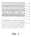
- FIG. 1 is a sectional view for use in describing production of a Bi layer structured ferroelectric thin film according to one embodiment of the present invention.
- a substrate to be used comprises a Si substrate 1, a silicon oxide 2 layer of SiO 2 formed by thermally oxidizing its surface, a lower electrode adhesive layer 3 of Ti on the silicon oxide layer, and a lower electrode 4 of Pt deposited by DC sputtering.
- an underlying base of the Bi layer structured ferroelectric thin film is formed on the surface.
- an oxide buffer layer 5 containing Bi is at first formed. Then, a Bi layer structured ferroelectric substance 6 is stacked on the surface of the buffer layer 5 to form the Bi layer structured ferroelectric thin film.
- a two-layered structure of the Bi layer structured ferroelectric thin film is formed by an additional step of stacking the Bi layer structured ferroelectric substance 6 on the surface of the buffer layer 5.
- a necessary heat treatment is carried out at a temperature not higher than 600°C or 700°C. Such a heat treatment serves to avoid degradation of characteristics in a device element in the Si substrate 1 due to a high temperature.
- the Bi layer structured ferroelectric layer 6 is processed in contact with the surface of the oxide buffer layer 5 containing Bi. As a result, deviation in Bi composition can be avoided within the Bi layer structured ferroelectric thin film thus produced.
- a substrate to be used comprises the Si substrate 1, the silicon oxide 2 layer of "SiO 2 " formed by thermally oxidizing its surface, the lower electrode adhesive layer 3 of Ti on the silicon oxide layer, and the lower electrode 4 of Pt deposited by DC sputtering.
- Sr and Bi as organic metal materials are mixed together at a stoichiometric ratio of SBO.
- the mixed materials are dissolved by an appropriate organic solvent to form the solution.
- organic metal materials containing Sr and Bi alkoxide and organic salt can be used, for example.
- the solvent use may be made of, for instance, 1-methoxy-2-propanol, organic acid, and xylene.
- diisopropoxystrontium and bismuth 2-ethylhexanoate were used as the organic metal materials.
- 2-ethylhexanoic acid and xylene were used. After each of the above-mentioned materials was weighed, these materials were circulated in a dry nitrogen atmosphere at 120°C for one hour. Thus, a coating solution having a concentration of 0.13 mol/kg was obtained.
- this solution was applied on the above-mentioned substrate by a spin coater of 1500 rpm, followed by necessary heat treatments. All of these heat treatments were carried out in an oxygen atmosphere. Specifically, drying of the solvent at 250°C for ten minutes, decomposition and removal of organic components at 400°C for ten minutes, and then crystallization annealing at 600°C or 700°C for one hour were successively carried out.
- FIG. 2 shows X-ray diffraction patterns of the SBO buffer layer after completion of the above-mentioned crystallization annealing.
- the indexed peaks illustrated in the figure may be considered from their positions as occurrence of crystallization of SBO. It is understood that SBO is crystallized by the heat treatment at 600°C or 700°C.
- a subsequent step is to form a thin film by the Bi layer structured ferroelectric substance 6.
- a coating solution to form an SBT thin film is prepared by the use of, for example, alkoxide or organic salt as the organic metal materials of Sr, Bi, and Ta along with the solvent, such as 1-methoxy-2-propanol, organic acid, and xylene.
- Diisopropoxy strontium, pentaethyoxy tantalum, and bismuth 2-ethylhexanoate were used as the organic metal materials.
- 2-ethylhexanoic acid and xylene were used as the solvent. After each of the above-mentioned materials was weighed, these materials were circulated in a dry nitrogen atmosphere at 120°C for one hour. Thus, a coating solution having a concentration of 0.13 mol/kg was obtained.
- this solution was applied on the above-mentioned substrate by a spin coater of 1500 rpm, followed by necessary heat treatments. All of these heat treatments were carried out in oxygen. Specifically, drying of the solvent at 250°C for ten minutes, decomposition and removal of organic components at 650°C for one hour, and then crystallization annealing at 650°C for one hour were successively carried out.
- the application and annealing processes of the SBO thin film as the buffer layer 5, and the application and annealing processes of the SBT thin film of the Bi layer structured ferroelectric substance 6 may be repeated a plurality of times until a desired thickness is achieved. In this manner, each time when the SBT thin film layer is formed, the SBO buffer layer 5 is formed prior to formation of the SBT thin film layer. Thus, an effective influence of each SBO buffer layer 5 is given to each SBT thin film layer.
- FIG. 3 shows an X-ray diffraction pattern of the SBT thin film obtained by the above-mentioned steps and that of the SBT thin film produced without the SBO buffer layer.
- a peak which may specify a fluorite phase is observed when the SBO buffer is absent.
- this phase is a paraelectric phase and does not exhibit ferroelectric characteristics.
- No peak is observed at the position corresponding to SBT of a Bi layer structured perovskite structure which has ferroelectricity. Therefore, a ferroelectric thin film is not obtained as desired.
- the SBO buffer layer is inserted, a peak is observed at the position corresponding to SBT of the Bi layer structured perovskite structure, which is a ferroelectric phase. It is, therefore, understood that the goal of a ferroelectric thin film can be obtained.
- the SBO buffer layer enhances the production of the Bi layer structured perovskite phase as the ferroelectric phase of the SBT.
- the structure of the crystal grain of the SBT thin film thus produced can be described as follows.
- columnar grains (crystalline state) having a grain size of about 0.1-0.2 ⁇ m were uniformly produced throughout the film surface.
- voids within the thin film are decreased.
- a second example will be described here with reference to FIG. 1.
- the concentration of the coating solution for the SBO buffer layer 5 was changed from 0.13 mol/kg of Example 1 to 0.02 mol/kg, and annealing for crystallization was carried out at 700°C. As a result, a SBO thin film having a thickness of about two nm was obtained as the buffer layer 5.
- FIG. 4 shows an X-ray diffraction pattern when the SBT thin film was produced on the SBO buffer layer 5 in a manner similar to that described in Example 1.
- the SBT thin film of the Bi layer structured perovskite structure is crystallized like in the above-mentioned first example.
- the crystallization of the Bi layer structured perovskite phase of the SBT thin film is enhanced.
- FIG. 5 shows a typical P-E hysteresis curve obtained when electrodes are formed on the surface of the thin film thus obtained and a sine wave of ⁇ 5 volts is applied therebetween.
- the crystal grain structure of the SBT thin film was not different from that of Example 1, in which the thickness of the SBO buffer layer was about 60 nm. It is noted that the leakage current density was reduced in comparison with that of the SBT thin film without the SBO buffer layer, listed under "Ref" in Table 1.
- a third example is described here with reference to FIG. 1.
- Annealing for crystallization was carried out at 600°C, instead of 700°C as in Example 2, and the concentration of the coating solution for the SBO buffer layer 5 was equal to 0.02 mol/kg.
- the SBO thin film obtained as the buffer layer 5 had a thickness of about two nm, as in Example 2.
- the SBT thin film was formed on the SBO buffer layer in the manner similar to that described in Example 1, the SBT thin film of the Bi layer structured perovskite structure was crystallized as in Example 2. It is, therefore, obvious that the crystallization of the BI layer structured perovskite phase of the SBT thin film was enhanced.
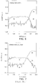
- FIGS. 6 and 7 show analysis results of the composition in depth direction in the SBT thin film structure with the SBO buffer layer produced in this example and in the SBT thin film structure formed on a Pt substrate at 800°C by a conventional method, respectively.
- the sample had a residual polarization of 4.0 ⁇ C/cm 2 measured at five volts.
- the residual polarization value is lower as compared with the case where the crystallization annealing of the SBO buffer layer was carried out at a temperature of 700°C, it is obvious that the SBT thin film produced by the method of this example exhibits ferroelectricity.
- the crystal grain structure of the SBT thin film is substantially identical with that of Example 1, in which the SBO buffer layer had a thickness of 60 nm.
- the Bi layer structured ferroelectric substance 6 is formed by RF ("radio frequency") magnetron sputtering on the substrate, after formation of the SBO buffer layer 5 thereon by the MOD method, as described in Example 3.
- RF radio frequency
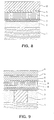
- the entire thin film can be crystallized at once, unlike the production by the MOD method. Therefore, as shown in FIG. 8, the SBO buffer layer 5 was able to be applied and baked only once on Pt formed on the substrate as the lower electrode 4. Therefore, the total thickness of the SBO buffer layer 5 was about two nm.
- the thin film obtained in this example had a residual polarization value of 5.1 ⁇ C/cm 2 .
- the ferroelectricity is clearly improved in comparison with the residual polarization value of 0.5 ⁇ C/cm 2 entered in Table 1 under "Ref" for the SBT thin film formed by MOD without the SBO buffer layer.
- BIT Bi 4 Ti 3 O 12
- the Bi layer structured ferroelectric thin film was formed by MOD using BIT and SBT as the buffer layer 5 and the Bi layer structured ferroelectric substance 6, respectively.
- Ti and Bi as organic metal materials mixed in a stoichiometric composition of BIT were dissolved by an appropriate organic solvent to form the BIT solution.
- organic metal materials for example, alkoxide and organic salt can be used.
- solvent use may be made of, for instance, 1-methoxy-2-propanol, organic acid and xylene.
- tetraisopropoxy titanium and bismuth 2-ethylhexanoate were used as organic metal materials, while 2-ethylhexanoic acid and xylene were used as solvents.
- This solution was applied as the buffer layer 5 on Pt formed as the lower electrode 4 of the substrate in FIG. 1 by a spin coater rotated at 1500 rpm, followed by necessary heat treatments. All of these heat treatments were carried out in an oxygen atmosphere. Specifically, drying of the solvent at 250°C for ten minutes, decomposition and removal of organic components at 400°C for ten minutes, and then crystallization annealing at 600°C for one hour were successively carried out. The resulting BIT buffer layer 5 was about seven nm thick.
- the SBT thin film was formed in a manner similar to that described in Example 1. This process was repeated twice together with the BIT deposition process. As a result, the BIT buffer layer had a total thickness of about 14 nm and the layer structure had a total thickness of about 210 nm.
- the capacitor had a residual polarization value of 4.5 ⁇ C/cm 2 . Therefore, it is obvious that the BIT buffer layer functions to enhance the crystallization of the Bi layer structured perovskite phase of the SBT, like the SBO buffer layer. Because the BIT buffer layer has a crystalline Bi layer structured perovskite structure as in SBT, the crystalline structure of the BIT is similar to that of the SBT and is also helpful to enhance the crystallization of SBT.
- the relative dielectric constant (120-140) is greater than that of the SBO buffer layer. Therefore, the ferroelectricity of the layer structure is not degraded, even if the thickness of the buffer layer becomes thick.
- the SBT thin film is composed of uniform and fine columnar grains having a diameter of about 0.1-0.2 ⁇ m.
- the BIT buffer layer 5 is formed by RF magnetron sputtering on Pt formed as the lower electrode 4 of the substrate of FIG. 1, as described in Example 5.
- the Bi layer structured ferroelectric thin film was formed by depositing the Bi layer structured ferroelectric substance 6 on the BIT buffer layer 5 of FIG. 1 using the MOD method.
- the production conditions are the same as in Example 1.
- the process of producing the BIT buffer layer arid the process of producing the Bi layer structured ferroelectric thin film using the MOD method with heat treatment for SBT crystallization were carried out twice.
- the BIT buffer layer measured had a total thickness of about ten nm, while the layer structure measured a total thickness of about 210 nm.
- the capacitor had a residual polarization value of 4.0 ⁇ C/cm 2 . Therefore, it is obvious that the BIT buffer layer formed by sputtering functions to enhance the crystallization of the Bi layer structured perovskite phase in the SBT thin film, similar to the BIT buffer layer formed by MOD.
- the crystal grain structure of the SBT thin film is similar to that of the SBT thin film on the BIT buffer layer formed by MOD, except that the crystal grain size is slightly smaller.
- This seventh example is described with reference to FIG. 9.
- a layer 9 of conductive-oxide forming metal is formed on the uppermost surface of the substrate on which the Bi layer structured ferroelectric thin film is to be formed on the surface of the oxide buffer layer 5 containing Bi.
- Ru ruthenium
- the conductive oxide forming metal 9 which can be used may be Ir or the like.
- the following steps were carried out in order to electrically connect the uppermost surface of the substrate to the Si substrate 1.
- the Si oxide layer 2 of SiO 2 was formed on the Si substrate 1.
- a contact hole was formed in the Si oxide film 2, a diffusion layer was formed.
- the contact hole was filled with polycrystalline Si 7.
- this polycrystalline Si 7 was etched by an etch back technique.
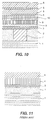
- Ti as the lower electrode adhesive layer 3, TiN layer 8, and Ru formed as the conductive oxide forming metal 9 were successively deposited by sputtering to 20 nm, 50 nm, and 50 nm thickness, respectively.
- the highest temperature of the heat treatment in oxygen atmosphere was 650°C.
- diffusion of oxygen from the surface inwards is prevented in the TiN layer 8 and the Ru layer as the conductive oxide forming metal 9. Therefore, the surface of the polycrystalline Si 7 or the TiN layer 8 is not oxidized. It is consequently possible to electrically connect the diffusion layer of the Si substrate 1 to the conductive oxide forming metal 9 of Ru formed on the uppermost surface of the substrate.
- the diffusion of Ru towards the inside of the Bi layer structured ferroelectric thin film 6 often becomes a problem when the thin film of the Bi layer structured ferroelectric substance 6 is formed on the surface of the conductive oxide forming metal 9 of Ru.
- such diffusion causes no problem at the temperature of 600°C at which the SBO buffer layer 5 is crystallized.
- the SBO buffer layer 5 serves as a barrier layer against the conductive oxide forming metal 9 of Ru, and thus prevents Ru from diffusing into SBT formed as the Bi layer structured ferroelectric substance 6. Accordingly, the characteristics of the Bi layer structured ferroelectric thin film are not degraded.
- the structure in this seventh example had a residual polarization value of 3.8 ⁇ C/cm 2 , which approximates that obtained in Example 3.
- a metal oxide layer 10 is formed on the uppermost surface of the substrate on which the Bi layer structured ferroelectric thin film is to be formed on the surface of the oxide buffer layer 5 containing Bi.
- ruthenium oxide, "RuO 2 " served as conductive oxide 10.
- RuO 2 served as conductive oxide 10.
- IrO 2 or the like may be used as the conductive oxide 10.
- sputtering was conducted to form Ru, as the conductive oxide forming metal 9, on the uppermost surface of the substrate, as in Example 7. Then a subsequent step was conducted by the use of reactive sputtering to further form "RuO 2 ", as the conductive oxide 10, on the above-mentioned surface.
- the SBO buffer layer 5 serves as a barrier layer against Ru and thus prevents Ru from diffusing into SBT formed as the Bi layer structured ferroelectric substance 6. Accordingly, the characteristics of the Bi layer structured ferroelectric thin film are not degraded.
- the structure in this example had a residual polarization value of 3.7 ⁇ C/cm 2 , which approximates that obtained in Example 3.
- Example 1 2 3 4 5 6 7 8 Ref Substrate Pt/Ti Pt/Ti Pt/Ti Pt/Ti Pt/Ti Pt/Ti Pt/Ti Ru RuO 2 Pt/Ti Buffer layer SBO SBO SBO SBO BIT BIT SBO SBO - Buffer layer producing method MOD MOD MOD MOD MOD SP MOD MOD MOD - Buffer layer preparation temperature (°C) 600/ 700 700 600 600 600 600 600 600 - Thickness of buffer layer (nm) 60 4 4 2 14 10 4 4 - Bi layer structured ferroelectric substance SBT SBT SBT SBT SBT SBT SBT SBT SBT SBT SBT SBT SBT SBT SBT SBT SBT SBT SBT SBT SBT SBT SBT SBT Producing method of Bi layer structured ferroelectric substance MOD MOD MOD SP MOD MOD MOD MOD MOD MOD MOD MOD MOD MOD Residual polarization ( ⁇ C/cm 2 )@5V 0 4.2 4.0 5.1 4.5 4.0 3.8 3.7
- SBO or BIT and SBT are used as the buffer layer and the Bi layer structured ferroelectric substance, respectively. It will be noted that a similar effect can be achieved by using BiTaO 4 as the buffer layer, and SrBi 2 Nb 2 O 9 , SrBi 2 (Nb 1 Ta 1 )O 9 , (Sr 0.9 Pb 0.1 )Bi 2 Ta 2 O 9 , or (Sr 0.9 Ba 0.1 )Bi 2 Ta 2 O 9 as the Bi layer structured ferroelectric substance.
- the buffer layer and the Bi layer structured ferroelectric layer use may be made of CVD (chemical vapor deposition), or laser ablation, instead of the MOD method and sputtering.
- CVD chemical vapor deposition
- laser ablation instead of the MOD method and sputtering.
- the crystallization temperature of the buffer layer is 600°C or 700°C in the examples described above, it has been confirmed that a similar effect can be achieved by steps of thermally decomposing the organic components after applying the buffer layer, thereafter forming the Bi layer structured ferroelectric thin film, and crystallizing the buffer layer when the Bi layer structured ferroelectric substance is subjected to the crystallization heat treatment.
- the buffer layer formed by the oxide thin film containing Bi is placed on the surface of the substrate and the Bi layer structured ferroelectric substance is deposited on the upper surface of the buffer layer, then to be crystallized.
- Bi contained in the above-mentioned buffer layer serves as a supply source compensating a lack of Bi within the Bi layer structured ferroelectric thin film arising from reaction of Bi with the precious metal of the lower electrode, which is located at a surface part during crystallization, or with the adhesive layer, or with the thermally oxidized Si underneath.
- the buffer layer is crystallized at a temperature not higher than 700°C.
- the reaction of Pt with Bi can be suppressed because the above-mentioned temperature is lower than about 730°C, at which a Bi-Pt compound is formed.
- the buffer layer and the Bi layer structured ferroelectric substance used for the Bi layer structured ferroelectric thin film are similar to each other in composition and structure. Therefore, the buffer layer acts as nucleation sites for crystallization of the Bi layer structured ferroelectric substance. This is effective to enhance the crystallization of the Bi layer structured ferroelectric thin film at a lower temperature and to form the fine grain structure.
- the buffer layer has a thickness not greater than five percent of that of the Bi layer structured ferroelectric thin film and can be used in a capacitor. Furthermore, the constituent elements of the buffer layer are partially similar to the constituent elements of the Bi layer structured ferroelectric substance. Therefore, during the formation of the Bi layer structured ferroelectric thin film, the buffer layer can be crystallized into the Bi layer structured ferroelectric thin film after the buffer layer finishes its role.
- the conductive oxide forming metal or a combination of the conductive oxide and "TiN" can be deposited on polycrystalline Si and serves as a barrier layer against diffusion of oxygen.
- the method of the invention may be used alone or in combination with other methods, devices and compositions intended to inhibit or reverse the detrimental effects of hydrogen degradation.
- the method of the invention is useful to prevent hydrogen degradation regardless of how it is caused. Reducing and other damaging conditions can arise in many circumstances during integrated circuit fabrication; even routine handling of the wafer can result in degradation of electronic properties.
Landscapes
- Semiconductor Memories (AREA)
- Inorganic Insulating Materials (AREA)
- Inorganic Compounds Of Heavy Metals (AREA)
- Formation Of Insulating Films (AREA)
- Non-Volatile Memory (AREA)
- Laminated Bodies (AREA)
- Crystals, And After-Treatments Of Crystals (AREA)
Applications Claiming Priority (3)
| Application Number | Priority Date | Filing Date | Title |
|---|---|---|---|
| JP28153197A JP3549715B2 (ja) | 1997-10-15 | 1997-10-15 | Bi層状強誘電体薄膜の製造方法 |
| JP281531/97 | 1997-10-15 | ||
| JP28153197 | 1997-10-15 |
Publications (2)
| Publication Number | Publication Date |
|---|---|
| EP0910120A2 true EP0910120A2 (de) | 1999-04-21 |
| EP0910120A3 EP0910120A3 (de) | 2000-02-02 |
Family
ID=17640480
Family Applications (1)
| Application Number | Title | Priority Date | Filing Date |
|---|---|---|---|
| EP98119403A Withdrawn EP0910120A3 (de) | 1997-10-15 | 1998-10-14 | Herstellungsverfahren für einen Bismuth enthaltenden dünnen ferroelektrischen Film |
Country Status (5)
| Country | Link |
|---|---|
| US (1) | US6194227B1 (de) |
| EP (1) | EP0910120A3 (de) |
| JP (1) | JP3549715B2 (de) |
| KR (1) | KR100478748B1 (de) |
| CN (1) | CN1114577C (de) |
Cited By (5)
| Publication number | Priority date | Publication date | Assignee | Title |
|---|---|---|---|---|
| WO2002017365A1 (de) * | 2000-08-24 | 2002-02-28 | Infineon Technologies Ag | Niedertemperatur-prozessierung ferroelektrischer strontium-wismuth-tantalat-schichten und herstellung ferroelektrischer bauelemente daraus |
| US6495878B1 (en) | 1999-08-02 | 2002-12-17 | Symetrix Corporation | Interlayer oxide containing thin films for high dielectric constant application |
| WO2003005433A3 (en) * | 2001-07-03 | 2003-05-30 | Matsushita Electric Industrial Co Ltd | Integrated circuit device including a layered superlattice material with an interface buffer layer |
| WO2004075296A1 (ja) * | 2003-02-19 | 2004-09-02 | Fujitsu Limited | 強誘電体キャパシタの製造方法 |
| US7312514B2 (en) | 2003-02-27 | 2007-12-25 | Tdk Corporation | High-permittivity insulation film, thin film capacity element, thin film multilayer capacitor, and production method of thin film capacity element |
Families Citing this family (19)
| Publication number | Priority date | Publication date | Assignee | Title |
|---|---|---|---|---|
| JP3520403B2 (ja) | 1998-01-23 | 2004-04-19 | セイコーエプソン株式会社 | 圧電体薄膜素子、アクチュエータ、インクジェット式記録ヘッド、及びインクジェット式記録装置 |
| JP3768357B2 (ja) * | 1998-12-01 | 2006-04-19 | 富士通株式会社 | 高誘電体キャパシタの製造方法 |
| JP2001237384A (ja) | 2000-02-22 | 2001-08-31 | Oki Electric Ind Co Ltd | 半導体装置の製造方法 |
| KR100612561B1 (ko) * | 2000-06-19 | 2006-08-11 | 주식회사 하이닉스반도체 | 반도체 소자의 캐패시터 제조 방법 |
| CN100441543C (zh) * | 2000-06-21 | 2008-12-10 | 精工爱普生株式会社 | 一种陶瓷膜的制造方法 |
| US7378719B2 (en) * | 2000-12-20 | 2008-05-27 | Micron Technology, Inc. | Low leakage MIM capacitor |
| KR20030039893A (ko) * | 2001-11-16 | 2003-05-22 | 주식회사 하이닉스반도체 | 반도체 소자의 캐패시터 및 그 제조방법 |
| US6876536B2 (en) * | 2002-12-27 | 2005-04-05 | Tdk Corporation | Thin film capacitor and method for fabricating the same |
| KR20040070564A (ko) * | 2003-02-04 | 2004-08-11 | 삼성전자주식회사 | 강유전체 커패시터 및 그 제조방법 |
| US6977806B1 (en) * | 2003-02-26 | 2005-12-20 | Tdk Corporation | Multi-layered unit including electrode and dielectric layer |
| US20040164416A1 (en) * | 2003-02-26 | 2004-08-26 | Tdk Corporation | Multi-layered unit |
| US6958900B2 (en) * | 2003-02-26 | 2005-10-25 | Tdk Corporation | Multi-layered unit including electrode and dielectric layer |
| US6891714B2 (en) * | 2003-02-26 | 2005-05-10 | Tdk Corporation | Multi-layered unit including electrode and dielectric layer |
| US7067458B2 (en) * | 2003-02-26 | 2006-06-27 | Tdk Corporation | Multi-layered unit including electrode and dielectric layer |
| US6885540B2 (en) * | 2003-02-26 | 2005-04-26 | Tdk Corporation | Multi-layered unit including electrode and dielectric layer |
| US20060237760A1 (en) * | 2003-02-27 | 2006-10-26 | Tdk Corporation | Thin-film capacitative element and electronic circuit and electronic equipment including the same |
| US6930875B2 (en) * | 2003-06-12 | 2005-08-16 | Tdk Corporation | Multi-layered unit |
| JP6308554B2 (ja) * | 2014-08-26 | 2018-04-11 | 国立研究開発法人物質・材料研究機構 | 誘電体薄膜 |
| CN112331620A (zh) * | 2020-11-04 | 2021-02-05 | 福建华佳彩有限公司 | 一种柔性薄膜封装结构及其制备方法 |
Family Cites Families (11)
| Publication number | Priority date | Publication date | Assignee | Title |
|---|---|---|---|---|
| US5519234A (en) | 1991-02-25 | 1996-05-21 | Symetrix Corporation | Ferroelectric dielectric memory cell can switch at least giga cycles and has low fatigue - has high dielectric constant and low leakage current |
| US5434102A (en) | 1991-02-25 | 1995-07-18 | Symetrix Corporation | Process for fabricating layered superlattice materials and making electronic devices including same |
| US5468679A (en) | 1991-02-25 | 1995-11-21 | Symetrix Corporation | Process for fabricating materials for ferroelectric, high dielectric constant, and integrated circuit applications |
| JP3113141B2 (ja) * | 1993-12-28 | 2000-11-27 | シャープ株式会社 | 強誘電体結晶薄膜被覆基板、その製造方法及び強誘電体結晶薄膜被覆基板を用いた強誘電体薄膜デバイス |
| US5426075A (en) * | 1994-06-15 | 1995-06-20 | Ramtron International Corporation | Method of manufacturing ferroelectric bismuth layered oxides |
| JP3363301B2 (ja) * | 1995-03-08 | 2003-01-08 | シャープ株式会社 | 強誘電体薄膜被覆基板及びその製造方法及び強誘電体薄膜被覆基板によって構成された不揮発性メモリ |
| US5833745A (en) * | 1995-11-15 | 1998-11-10 | Mitsubishi Materials Corporation | Bi-based ferroelectric composition and thin film, method for forming the thin film, and non-volatile memory |
| JP3180642B2 (ja) | 1995-11-29 | 2001-06-25 | 三菱マテリアル株式会社 | Bi系強誘電体薄膜及びその形成方法 |
| US5824590A (en) * | 1996-07-23 | 1998-10-20 | Micron Technology, Inc. | Method for oxidation and crystallization of ferroelectric material |
| US5784310A (en) | 1997-03-03 | 1998-07-21 | Symetrix Corporation | Low imprint ferroelectric material for long retention memory and method of making the same |
| US5902639A (en) * | 1997-03-31 | 1999-05-11 | Advanced Technology Materials, Inc | Method of forming bismuth-containing films by using bismuth amide compounds |
-
1997
- 1997-10-15 JP JP28153197A patent/JP3549715B2/ja not_active Expired - Fee Related
-
1998
- 1998-10-14 US US09/174,393 patent/US6194227B1/en not_active Expired - Lifetime
- 1998-10-14 CN CN98120287A patent/CN1114577C/zh not_active Expired - Fee Related
- 1998-10-14 EP EP98119403A patent/EP0910120A3/de not_active Withdrawn
- 1998-10-15 KR KR10-1998-0043173A patent/KR100478748B1/ko not_active Expired - Fee Related
Cited By (8)
| Publication number | Priority date | Publication date | Assignee | Title |
|---|---|---|---|---|
| US6495878B1 (en) | 1999-08-02 | 2002-12-17 | Symetrix Corporation | Interlayer oxide containing thin films for high dielectric constant application |
| US6541279B2 (en) | 1999-08-02 | 2003-04-01 | Symetrix Corporation | Method for forming an integrated circuit |
| US6867452B2 (en) | 1999-08-02 | 2005-03-15 | Symetrix Corporation | Interlayer oxide containing thin films for high dielectric constant application of the formula AB2O6 or AB2O7 |
| WO2002017365A1 (de) * | 2000-08-24 | 2002-02-28 | Infineon Technologies Ag | Niedertemperatur-prozessierung ferroelektrischer strontium-wismuth-tantalat-schichten und herstellung ferroelektrischer bauelemente daraus |
| US6815224B2 (en) | 2000-08-24 | 2004-11-09 | Infineon Technologies Ag | Low-temperature processing of a ferroelectric strontium bismuth tantalate layer, and fabrication of ferroelectric components using the layer |
| WO2003005433A3 (en) * | 2001-07-03 | 2003-05-30 | Matsushita Electric Industrial Co Ltd | Integrated circuit device including a layered superlattice material with an interface buffer layer |
| WO2004075296A1 (ja) * | 2003-02-19 | 2004-09-02 | Fujitsu Limited | 強誘電体キャパシタの製造方法 |
| US7312514B2 (en) | 2003-02-27 | 2007-12-25 | Tdk Corporation | High-permittivity insulation film, thin film capacity element, thin film multilayer capacitor, and production method of thin film capacity element |
Also Published As
| Publication number | Publication date |
|---|---|
| JP3549715B2 (ja) | 2004-08-04 |
| US6194227B1 (en) | 2001-02-27 |
| CN1114577C (zh) | 2003-07-16 |
| CN1216296A (zh) | 1999-05-12 |
| KR100478748B1 (ko) | 2005-09-12 |
| EP0910120A3 (de) | 2000-02-02 |
| JPH11121703A (ja) | 1999-04-30 |
| KR19990037121A (ko) | 1999-05-25 |
Similar Documents
| Publication | Publication Date | Title |
|---|---|---|
| US6194227B1 (en) | Method of producing a bismuth layer structured ferroelectric thin film | |
| JP3188179B2 (ja) | 強誘電体薄膜素子の製造方法及び強誘電体メモリ素子の製造方法 | |
| US5439845A (en) | Process for fabricating layered superlattice materials and making electronic devices including same | |
| US6194228B1 (en) | Electronic device having perovskite-type oxide film, production thereof, and ferroelectric capacitor | |
| EP0815588B1 (de) | Niedrig-temperatur-verfahren zur herstellung von geschichteten supergittermaterialen | |
| EP0665981B1 (de) | Herstellungsverfahren von geschichteten uebergittermaterialien und von diesen enthaltenden elektronischen vorrichtungen | |
| US7001778B2 (en) | Method of making layered superlattice material with improved microstructure | |
| EP0747938B1 (de) | Mit einer dünnen ferreoelektrischen Schicht überdecktes Substrat, Verfahren zu seiner Herstellung und in diesem verwendende Kondensator-Struktur | |
| KR20010031913A (ko) | 유전체 소자와 그 제조 방법 | |
| US20040101977A1 (en) | Low thermal budget fabrication of ferroelectric memory using RTP | |
| US6338970B1 (en) | Ferroelectric capacitor of semiconductor device and method for fabricating the same | |
| US6127218A (en) | Methods for forming ferroelectric films using dual deposition steps | |
| US6437380B1 (en) | Ferroelectric device with bismuth tantalate capping layer and method of making same | |
| US20030230773A1 (en) | Ferroelectric capacitor, process for manufacturing thereof and ferroelectric memory | |
| US6309896B1 (en) | Method of manufacturing a ferroelectric film | |
| US7217576B2 (en) | Method for manufacturing ferroelectric capacitor, method for manufacturing ferroelectric memory, ferroelectric capacitor and ferroelectric memory | |
| JPH09129827A (ja) | 強誘電体キャパシタ | |
| JP4416230B2 (ja) | 電子装置の製造方法 | |
| KR20090052455A (ko) | 강유전체 캐패시터 및 이의 제조 방법 | |
| EP1077478B1 (de) | Herstellungsmethode für einen ferroelektrischen dünnen Film, einen ferroelektrischen Kondensator und einen ferroelektrischen Speicher | |
| US6884674B2 (en) | Method for fabricating a semiconductor device including a capacitance insulating film having a perovskite structure | |
| JPH11186510A (ja) | 強誘電体キャパシタの形成方法及び不揮発性半導体記憶素子の製造方法 | |
| KR100438769B1 (ko) | 화학 기상증착 방법을 이용한 반도체장치의 금속 산화물 박막 형성방법 및 이를 이용한 커패시터 형성방법 | |
| JP2007081410A (ja) | 強誘電体膜及び強誘電体キャパシタ形成方法及び強誘電体キャパシタ | |
| KR19980082338A (ko) | 배향성이 제어되는 백금 박막과 그러한 백금 박막을 구비한 전자 소자의 제조 방법 및 그 방법에 의해 형성된 백금 박막과 백금 박막이 구비된 전자 소자 |
Legal Events
| Date | Code | Title | Description |
|---|---|---|---|
| PUAI | Public reference made under article 153(3) epc to a published international application that has entered the european phase |
Free format text: ORIGINAL CODE: 0009012 |
|
| AK | Designated contracting states |
Kind code of ref document: A2 Designated state(s): DE FR GB IT NL |
|
| AX | Request for extension of the european patent |
Free format text: AL;LT;LV;MK;RO;SI |
|
| PUAL | Search report despatched |
Free format text: ORIGINAL CODE: 0009013 |
|
| RIC1 | Information provided on ipc code assigned before grant |
Free format text: 7H 01L 21/316 A, 7H 01L 21/02 B |
|
| AK | Designated contracting states |
Kind code of ref document: A3 Designated state(s): AT BE CH CY DE DK ES FI FR GB GR IE IT LI LU MC NL PT SE |
|
| AX | Request for extension of the european patent |
Free format text: AL;LT;LV;MK;RO;SI |
|
| 17P | Request for examination filed |
Effective date: 20000105 |
|
| AKX | Designation fees paid |
Free format text: DE FR GB IT NL |
|
| 17Q | First examination report despatched |
Effective date: 20061002 |
|
| GRAP | Despatch of communication of intention to grant a patent |
Free format text: ORIGINAL CODE: EPIDOSNIGR1 |
|
| STAA | Information on the status of an ep patent application or granted ep patent |
Free format text: STATUS: THE APPLICATION HAS BEEN WITHDRAWN |
|
| 18W | Application withdrawn |
Effective date: 20090604 |