EP0913932A2 - Integrierte Pufferschaltung - Google Patents
Integrierte Pufferschaltung Download PDFInfo
- Publication number
- EP0913932A2 EP0913932A2 EP19980308565 EP98308565A EP0913932A2 EP 0913932 A2 EP0913932 A2 EP 0913932A2 EP 19980308565 EP19980308565 EP 19980308565 EP 98308565 A EP98308565 A EP 98308565A EP 0913932 A2 EP0913932 A2 EP 0913932A2
- Authority
- EP
- European Patent Office
- Prior art keywords
- voltage
- input
- mosfet
- buffering
- source
- Prior art date
- Legal status (The legal status is an assumption and is not a legal conclusion. Google has not performed a legal analysis and makes no representation as to the accuracy of the status listed.)
- Withdrawn
Links
- 230000003139 buffering effect Effects 0.000 title claims abstract description 31
- 238000010586 diagram Methods 0.000 description 6
- 238000000034 method Methods 0.000 description 4
- 230000005669 field effect Effects 0.000 description 1
- 229910044991 metal oxide Inorganic materials 0.000 description 1
- 150000004706 metal oxides Chemical class 0.000 description 1
- 239000004065 semiconductor Substances 0.000 description 1
Images

Classifications
-
- H—ELECTRICITY
- H03—ELECTRONIC CIRCUITRY
- H03F—AMPLIFIERS
- H03F3/00—Amplifiers with only discharge tubes or only semiconductor devices as amplifying elements
- H03F3/50—Amplifiers in which input is applied to, or output is derived from, an impedance common to input and output circuits of the amplifying element, e.g. cathode follower
- H03F3/505—Amplifiers in which input is applied to, or output is derived from, an impedance common to input and output circuits of the amplifying element, e.g. cathode follower with field-effect devices
-
- H—ELECTRICITY
- H03—ELECTRONIC CIRCUITRY
- H03F—AMPLIFIERS
- H03F3/00—Amplifiers with only discharge tubes or only semiconductor devices as amplifying elements
- H03F3/34—DC amplifiers in which all stages are DC-coupled
- H03F3/343—DC amplifiers in which all stages are DC-coupled with semiconductor devices only
- H03F3/347—DC amplifiers in which all stages are DC-coupled with semiconductor devices only in integrated circuits
Definitions
- This invention relates generally to a buffering circuit and more particularly concerns a buffering integrated circuit with a buffer which receives a shifted down version of a voltage which requires to be buffered and outputs a voltage which is substantially equal to the original value of the voltage which needs to be buffered.
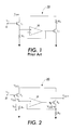
- FIG. 1 there is shown a prior art buffering circuit diagram 10 which shifts down a voltage prior to a buffer (Op-Amp) 14 and shifts it back up after buffer 14.
- node 12 has a voltage V 1 which needs to be buffered.
- voltage V 1 has to be shifted down.
- node 12 is connected to the gate of a Metal Oxide Semiconductor Field Effect Transistor (MOSFET) T 1 .
- MOSFET Metal Oxide Semiconductor Field Effect Transistor
- the drain of transistor T 1 is connected to a power supply V DD and its source is grounded through resistor R 1 .
- MOSFET Metal Oxide Semiconductor Field Effect Transistor
- the source of transistor T 1 is connected to the non-inverting input of Op-Amp 14.
- the inverting input of Op-Amp 14 is connected to its output which is connected to the gate of the transistor T 2 .
- Op-Amp 14 delivers its non-inverting input to its output and therefrom to the gate of transistor T 2 .
- a PMOS transistor T 2 is used.
- V S2 V G2 - V GS2
- 1 ⁇ 2V GS2 1 ⁇ 2 is the absolute value of the V GS2 which has a negative value for PMOS transistors.
- transistor T 1 is a NMOS and transistor T 2 is a PMOS, even if the source current I S1 of transistor T1 and the source current I S2 of transistor T2 are kept the same, the gate to source voltages V GS1 and V GS2 are not exactly the same. This is due to the fact that transistors T 1 and T 2 are different type transistors and they do not have similar characteristics. Therefore, the source voltage V S2 of the transistor T 2 which is the voltage that has been shifted up, is not exactly equal to V 1 .
- a buffering integrated circuit which utilizes an Op-Amp and two MOSFETs for level shifting down and up.
- the source of the first MOSFET is connected to a first input of the Op-Amp and the source of the second MOSFET is connected to the second input of the Op-Amp and the output of the Op-Amp is connected to the gate of the second MOSFET.
- the first MOSFET receives a voltage and shifts it down and delivers it to the first input of the Op-Amp.
- the second MOSFET causes its gate and the output of the Op-Amp to be substantially equal to the received voltage by the first MOSFET.
- node 22 has a voltage V 3 which needs to be buffered. Voltage V 3 is shifted down to match the input voltage of an Op-Amp 24.
- node 22 is connected to the gate of MOSFET T 3 which is used as a level shifter.
- the drain of transistor T 3 is connected to a power supply V DD1 and its source is connected to ground through resistor R 3 .
- Transistor T 3 shifts down the voltage of its gate V G3 to the source voltage V S3 by the gate to source voltage V GS3 .
- V S3 of the transistor T 3 V G3 - V GS3
- V S3 V 3 - V GS3
- transistor T 3 shifts down voltage V 3 by V GS3 to V S3 .
- V S3 is also called V 3(shifted down)
- the source of transistor T 3 is connected to non-inverting input of Op-Amp 24.
- the output of Op-Amp 24 is connected to the gate of the transistor T 4 .
- the drain of transistor T 4 is connected to the power supply V DD1 and the source of transistor T 4 is grounded through a resistor R4.
- resistors R 3 and R 4 are selected in such a manner that the source current I S3 of transistor T 3 and the source current I S4 of transistor T 4 are equal.
- Op-Amp 24 delivers its non-inverting input to its output and therefrom to the gate of transistor T 4 .
- its output voltage needs to be shifted back to the original value of V 3 .
- a NMOS transistor T 4 is used in order to shift back the voltage V 3(shifted down) to voltage V 3 .
- transistor T 4 is used to guide the output of Op-Amp 24 to be shifted up.
- Both transistors T 3 and T 4 are NMOS transistors and they both are made with the same process and in the layout they are placed close to each other to minimize the process variation of different locations on the wafer.
- the gate to source voltages (threshold voltages) V GS3 and V GS4 of the two transistors T 3 and T 4 are substantially the same since the transistors T 3 and T 4 have identical sizes and currents.
- V G4 V S4 + V GS4
- V S3 V S4 (source voltage of T 4 is set by Op-Amp 24 to be equal to source voltage of T 3 )
- V GS3 V GS4 (two identical transistors T 3 and T 4 have same currents)
- the output is obtained from the gate of transistor T4 which is also the output of the Op-Amp 24 and is buffered by the Op-Amp 24.
- the output voltage V OUT can be modified. This can be used in such applications which may require a voltage higher than the inverting or non-inverting input voltages of the Op-Amp 24 but not equal to the voltage V 3 of node 22.
- FIG. 3 there is shown an alternative circuit 30 of this invention which is the same as circuit 20 of Figure 2 except the passive loads R 3 and R 4 of Figure 2 are replaced by a current mirror 40. All the elements of circuit 30 which are the same as the elements of circuit 20 are designated the same reference numerals.
- the current mirror 40 comprises three NMOS transistors T 5 , T 6 , and T 7 .
- the sources of transistors T 5 , T 6 and T 7 are all grounded and the gates of transistors T 5 , T 6 and T 7 are connected to each other.
- the drain of transistor T 5 is connected to the source of transistor T 4 and the drain of transistor T 6 is connected to the source of transistor T 3 .
- the drain of transistor T 7 is connected to its gate and also to the power supply V DD1 through resistor R 5 .
- Transistor T 7 generates a current I and transistors T 5 and T 6 force the currents I S33 and I S44 to be identical to the current I. Therefore, the source current I S33 of transistor T 3 and the source current I S44 of transistor T 4 are identical.
- the disclosed embodiments of this invention shift down a voltage which needs to be buffered and shift it up substantially to its original value.
- FIG. 4 there is shown a buffering integrated circuit diagram 40 of this invention which shifts up voltage V 4 to match the requirements of Op-Amp 44 and subsequently shifts down the shifted up voltage back to its original value.
- transistor T 8 shifts up the voltage V 4 and transistor T 9 causes the voltage V OUT2 of its gate and the output of Op-Amp 44 to be substantially equal to V 4 .
- transistors T 8 and T 9 are PMOS transistors.
- the output voltage V OUT2 can be modified. This can be used in such applications that may require a voltage lower than the inverting or non-inverting input voltages of the Op-Amp 24 but not equal to the voltage V 4 of node 42.
Landscapes
- Engineering & Computer Science (AREA)
- Power Engineering (AREA)
- Microelectronics & Electronic Packaging (AREA)
- Logic Circuits (AREA)
- Amplifiers (AREA)
Applications Claiming Priority (2)
| Application Number | Priority Date | Filing Date | Title |
|---|---|---|---|
| US96070597A | 1997-10-30 | 1997-10-30 | |
| US960705 | 1997-10-30 |
Publications (1)
| Publication Number | Publication Date |
|---|---|
| EP0913932A2 true EP0913932A2 (de) | 1999-05-06 |
Family
ID=25503512
Family Applications (1)
| Application Number | Title | Priority Date | Filing Date |
|---|---|---|---|
| EP19980308565 Withdrawn EP0913932A2 (de) | 1997-10-30 | 1998-10-20 | Integrierte Pufferschaltung |
Country Status (2)
| Country | Link |
|---|---|
| EP (1) | EP0913932A2 (de) |
| JP (1) | JPH11214934A (de) |
Cited By (2)
| Publication number | Priority date | Publication date | Assignee | Title |
|---|---|---|---|---|
| EP1388926A1 (de) * | 2002-08-05 | 2004-02-11 | Matsushita Electric Industrial Co., Ltd. | Pegelschiebender Spannungsgenerator |
| EP3282581A1 (de) * | 2016-08-05 | 2018-02-14 | MediaTek Inc. | Pufferstufe und steuerschaltung |
Families Citing this family (1)
| Publication number | Priority date | Publication date | Assignee | Title |
|---|---|---|---|---|
| JP4104012B2 (ja) | 2005-03-10 | 2008-06-18 | 株式会社半導体理工学研究センター | 電流ミラー回路 |
-
1998
- 1998-10-20 EP EP19980308565 patent/EP0913932A2/de not_active Withdrawn
- 1998-10-21 JP JP10299750A patent/JPH11214934A/ja not_active Withdrawn
Cited By (3)
| Publication number | Priority date | Publication date | Assignee | Title |
|---|---|---|---|---|
| EP1388926A1 (de) * | 2002-08-05 | 2004-02-11 | Matsushita Electric Industrial Co., Ltd. | Pegelschiebender Spannungsgenerator |
| EP3282581A1 (de) * | 2016-08-05 | 2018-02-14 | MediaTek Inc. | Pufferstufe und steuerschaltung |
| US10613560B2 (en) | 2016-08-05 | 2020-04-07 | Mediatek Inc. | Buffer stage and control circuit |
Also Published As
| Publication number | Publication date |
|---|---|
| JPH11214934A (ja) | 1999-08-06 |
Similar Documents
| Publication | Publication Date | Title |
|---|---|---|
| US6563371B2 (en) | Current bandgap voltage reference circuits and related methods | |
| US5446396A (en) | Voltage comparator with hysteresis | |
| JPH06326595A (ja) | インターフェース回路及び低電圧信号受信回路 | |
| US6747514B1 (en) | MOSFET amplifier with dynamically biased cascode output | |
| US5959446A (en) | High swing current efficient CMOS cascode current mirror | |
| JP4117780B2 (ja) | 基準電圧回路および電子機器 | |
| JP2005018783A (ja) | 一定の基準電流を発生させるための電流源 | |
| US20060097769A1 (en) | Level shift circuit and semiconductor circuit device including the level shift circuit | |
| WO1991005404A2 (en) | Current mirror | |
| US6184745B1 (en) | Reference voltage generating circuit | |
| US6717451B1 (en) | Precision analog level shifter with programmable options | |
| US8482321B2 (en) | Input circuit and semiconductor integrated circuit including the same | |
| EP0913932A2 (de) | Integrierte Pufferschaltung | |
| US6181195B1 (en) | Impedance transport circuit | |
| US6323725B1 (en) | Constant transconductance bias circuit having body effect cancellation circuitry | |
| US6825718B2 (en) | Impedance matching circuit | |
| US5598094A (en) | Current mirror | |
| US7436214B2 (en) | Pseudo differential current mode receiver | |
| EP1017164A2 (de) | Stromspiegel mit einem konstanten Strom über einen weiten Bereich der Ausgangslastimpedanz | |
| JPH07191065A (ja) | 集積コンパレータ回路 | |
| US20100073037A1 (en) | Output impedance control circuit | |
| JP4359709B2 (ja) | 基準電圧発生装置 | |
| JPH08293745A (ja) | Cmis差動増幅回路 | |
| JPH0685584A (ja) | 比較器 | |
| KR100330094B1 (ko) | 밴드캡레퍼런스를이용한바이어스회로 |
Legal Events
| Date | Code | Title | Description |
|---|---|---|---|
| PUAI | Public reference made under article 153(3) epc to a published international application that has entered the european phase |
Free format text: ORIGINAL CODE: 0009012 |
|
| AK | Designated contracting states |
Kind code of ref document: A2 Designated state(s): AT BE CH CY DE DK ES FI FR GB GR IE IT LI LU MC NL PT SE |
|
| AX | Request for extension of the european patent |
Free format text: AL;LT;LV;MK;RO;SI |
|
| STAA | Information on the status of an ep patent application or granted ep patent |
Free format text: STATUS: THE APPLICATION HAS BEEN WITHDRAWN |
|
| 18W | Application withdrawn |
Withdrawal date: 19990902 |