EP0915516A2 - Substrat pour module empilé et module empilé - Google Patents
Substrat pour module empilé et module empilé Download PDFInfo
- Publication number
- EP0915516A2 EP0915516A2 EP98120397A EP98120397A EP0915516A2 EP 0915516 A2 EP0915516 A2 EP 0915516A2 EP 98120397 A EP98120397 A EP 98120397A EP 98120397 A EP98120397 A EP 98120397A EP 0915516 A2 EP0915516 A2 EP 0915516A2
- Authority
- EP
- European Patent Office
- Prior art keywords
- chip select
- electrodes
- electrode
- substrates
- substrate
- Prior art date
- Legal status (The legal status is an assumption and is not a legal conclusion. Google has not performed a legal analysis and makes no representation as to the accuracy of the status listed.)
- Withdrawn
Links
Images


Classifications
-
- H—ELECTRICITY
- H05—ELECTRIC TECHNIQUES NOT OTHERWISE PROVIDED FOR
- H05K—PRINTED CIRCUITS; CASINGS OR CONSTRUCTIONAL DETAILS OF ELECTRIC APPARATUS; MANUFACTURE OF ASSEMBLAGES OF ELECTRICAL COMPONENTS
- H05K1/00—Printed circuits
- H05K1/02—Details
- H05K1/14—Structural association of two or more printed circuits
- H05K1/144—Stacked arrangements of planar printed circuit boards
-
- H—ELECTRICITY
- H05—ELECTRIC TECHNIQUES NOT OTHERWISE PROVIDED FOR
- H05K—PRINTED CIRCUITS; CASINGS OR CONSTRUCTIONAL DETAILS OF ELECTRIC APPARATUS; MANUFACTURE OF ASSEMBLAGES OF ELECTRICAL COMPONENTS
- H05K1/00—Printed circuits
- H05K1/02—Details
- H05K1/11—Printed elements for providing electric connections to or between printed circuits
- H05K1/111—Pads for surface mounting, e.g. lay-out
- H05K1/112—Pads for surface mounting, e.g. lay-out directly combined with via connections
-
- H—ELECTRICITY
- H10—SEMICONDUCTOR DEVICES; ELECTRIC SOLID-STATE DEVICES NOT OTHERWISE PROVIDED FOR
- H10W—GENERIC PACKAGES, INTERCONNECTIONS, CONNECTORS OR OTHER CONSTRUCTIONAL DETAILS OF DEVICES COVERED BY CLASS H10
- H10W90/00—Package configurations
-
- H—ELECTRICITY
- H10—SEMICONDUCTOR DEVICES; ELECTRIC SOLID-STATE DEVICES NOT OTHERWISE PROVIDED FOR
- H10W—GENERIC PACKAGES, INTERCONNECTIONS, CONNECTORS OR OTHER CONSTRUCTIONAL DETAILS OF DEVICES COVERED BY CLASS H10
- H10W90/00—Package configurations
- H10W90/401—Package configurations characterised by multiple insulating or insulated package substrates, interposers or RDLs
-
- H—ELECTRICITY
- H10—SEMICONDUCTOR DEVICES; ELECTRIC SOLID-STATE DEVICES NOT OTHERWISE PROVIDED FOR
- H10W—GENERIC PACKAGES, INTERCONNECTIONS, CONNECTORS OR OTHER CONSTRUCTIONAL DETAILS OF DEVICES COVERED BY CLASS H10
- H10W90/00—Package configurations
- H10W90/701—Package configurations characterised by the relative positions of pads or connectors relative to package parts
-
- H—ELECTRICITY
- H10—SEMICONDUCTOR DEVICES; ELECTRIC SOLID-STATE DEVICES NOT OTHERWISE PROVIDED FOR
- H10W—GENERIC PACKAGES, INTERCONNECTIONS, CONNECTORS OR OTHER CONSTRUCTIONAL DETAILS OF DEVICES COVERED BY CLASS H10
- H10W72/00—Interconnections or connectors in packages
- H10W72/01—Manufacture or treatment
-
- H—ELECTRICITY
- H10—SEMICONDUCTOR DEVICES; ELECTRIC SOLID-STATE DEVICES NOT OTHERWISE PROVIDED FOR
- H10W—GENERIC PACKAGES, INTERCONNECTIONS, CONNECTORS OR OTHER CONSTRUCTIONAL DETAILS OF DEVICES COVERED BY CLASS H10
- H10W72/00—Interconnections or connectors in packages
- H10W72/071—Connecting or disconnecting
- H10W72/072—Connecting or disconnecting of bump connectors
- H10W72/07251—Connecting or disconnecting of bump connectors characterised by changes in properties of the bump connectors during connecting
-
- H—ELECTRICITY
- H10—SEMICONDUCTOR DEVICES; ELECTRIC SOLID-STATE DEVICES NOT OTHERWISE PROVIDED FOR
- H10W—GENERIC PACKAGES, INTERCONNECTIONS, CONNECTORS OR OTHER CONSTRUCTIONAL DETAILS OF DEVICES COVERED BY CLASS H10
- H10W72/00—Interconnections or connectors in packages
- H10W72/20—Bump connectors, e.g. solder bumps or copper pillars; Dummy bumps; Thermal bumps
- H10W72/241—Dispositions, e.g. layouts
- H10W72/244—Dispositions, e.g. layouts relative to underlying supporting features, e.g. bond pads, RDLs or vias
-
- H—ELECTRICITY
- H10—SEMICONDUCTOR DEVICES; ELECTRIC SOLID-STATE DEVICES NOT OTHERWISE PROVIDED FOR
- H10W—GENERIC PACKAGES, INTERCONNECTIONS, CONNECTORS OR OTHER CONSTRUCTIONAL DETAILS OF DEVICES COVERED BY CLASS H10
- H10W72/00—Interconnections or connectors in packages
- H10W72/20—Bump connectors, e.g. solder bumps or copper pillars; Dummy bumps; Thermal bumps
- H10W72/29—Bond pads specially adapted therefor
-
- H—ELECTRICITY
- H10—SEMICONDUCTOR DEVICES; ELECTRIC SOLID-STATE DEVICES NOT OTHERWISE PROVIDED FOR
- H10W—GENERIC PACKAGES, INTERCONNECTIONS, CONNECTORS OR OTHER CONSTRUCTIONAL DETAILS OF DEVICES COVERED BY CLASS H10
- H10W72/00—Interconnections or connectors in packages
- H10W72/90—Bond pads, in general
- H10W72/921—Structures or relative sizes of bond pads
- H10W72/922—Bond pads being integral with underlying chip-level interconnections
-
- H—ELECTRICITY
- H10—SEMICONDUCTOR DEVICES; ELECTRIC SOLID-STATE DEVICES NOT OTHERWISE PROVIDED FOR
- H10W—GENERIC PACKAGES, INTERCONNECTIONS, CONNECTORS OR OTHER CONSTRUCTIONAL DETAILS OF DEVICES COVERED BY CLASS H10
- H10W72/00—Interconnections or connectors in packages
- H10W72/90—Bond pads, in general
- H10W72/941—Dispositions of bond pads
- H10W72/942—Dispositions of bond pads relative to underlying supporting features, e.g. bond pads, RDLs or vias
-
- H—ELECTRICITY
- H10—SEMICONDUCTOR DEVICES; ELECTRIC SOLID-STATE DEVICES NOT OTHERWISE PROVIDED FOR
- H10W—GENERIC PACKAGES, INTERCONNECTIONS, CONNECTORS OR OTHER CONSTRUCTIONAL DETAILS OF DEVICES COVERED BY CLASS H10
- H10W90/00—Package configurations
- H10W90/20—Configurations of stacked chips
- H10W90/22—Configurations of stacked chips the stacked chips being on both top and bottom sides of a package substrate, interposer or RDL
-
- H—ELECTRICITY
- H10—SEMICONDUCTOR DEVICES; ELECTRIC SOLID-STATE DEVICES NOT OTHERWISE PROVIDED FOR
- H10W—GENERIC PACKAGES, INTERCONNECTIONS, CONNECTORS OR OTHER CONSTRUCTIONAL DETAILS OF DEVICES COVERED BY CLASS H10
- H10W90/00—Package configurations
- H10W90/20—Configurations of stacked chips
- H10W90/297—Configurations of stacked chips characterised by the through-semiconductor vias [TSVs] in the stacked chips
-
- H—ELECTRICITY
- H10—SEMICONDUCTOR DEVICES; ELECTRIC SOLID-STATE DEVICES NOT OTHERWISE PROVIDED FOR
- H10W—GENERIC PACKAGES, INTERCONNECTIONS, CONNECTORS OR OTHER CONSTRUCTIONAL DETAILS OF DEVICES COVERED BY CLASS H10
- H10W90/00—Package configurations
- H10W90/701—Package configurations characterised by the relative positions of pads or connectors relative to package parts
- H10W90/721—Package configurations characterised by the relative positions of pads or connectors relative to package parts of bump connectors
- H10W90/722—Package configurations characterised by the relative positions of pads or connectors relative to package parts of bump connectors between stacked chips
Definitions
- This invention relates to a packaging structure in which a semiconductor device such as a memory or the like is used, and particularly to a stacked module formed by stacking semiconductor devices and connecting them and substrates used for the stacked module, in which a semiconductor device is mounted on the surface thereof, to be stacked.
- a known packaging method for a semiconductor device is that a semiconductor device is mounted on a substrate, the substrates are stacked in plural layers to construct a stacked module, and the module is mounted on a motherboard.
- This packaging for a semiconductor device by the stacked module is effective for reducing the packaging area.
- the stacked module using a substrate is effectively utilized for packaging a semiconductor chip such as a semiconductor memory or the like.
- a semiconductor chip such as a semiconductor memory or the like.
- DRAM dynamic RAMs
- FIG. 10 the external terminals of the DRAM 80, 81 are all shared except RAS (Row Address Strobe).
- RAS Row Address Strobe
- the terminals 82, 83 connected to RAS are separately used for chip select. Chip select may be performed not by RAS, but by CAS (Column Address Strobe).
- terminals other than a chip select terminal for determining which DRAMs 80, 81 is operated are shared, thus in the case of wiring packaging, substrates on which DRAMs are mounted can be stacked.
- the stacked module is, for example, as described in Japan Patent Laid-Open No. 8-236694, such that a plurality of substrates (carrier) where a semiconductor chip (LSI chip) is mounted facedown are stacked and connection between the substrates is performed by metallic pins or conductive bumps.
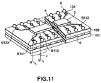
- FIG. 11 is a perspective view showing this type of a stacked module using conductive bumps.
- the stacked module of FIG. 11 is equivalent to a memory circuit of FIG. 10.
- semiconductor chips 3, 4 are respectively chips of DRAMs 80, 81 of FIG. 10.
- the semiconductor chips 3, 4 are mounted facedown on substrates 100, 101.
- the matrix of the substrates 100, 101 is formed by an insulator such as ceramics, glass or the like.
- a conductive bump 5 is mounted on each electrode pad of the substrate 100, a conductive bump 6 is mounted on each electrode pad of the substrate 101, and the respective electrode pads are wired to terminals (not shown) of the semiconductor chips 3, 4. Connection between the substrates 100, 101 is performed through the conductive bumps 6.
- the conductive bumps 5 are served as external terminals at the time of connecting the stacked module of FIG. 11 facedown to a motherboard not shown.
- FIG. 12A shows the upper substrate 100 where the semiconductor chip 3 is mounted
- FIG. 12B shows the lower substrate 101 where the semiconductor chip 4 is mounted
- they are plan views respectively showing the condition before the conductive bumps 5, 6 are mounted.
- Electrode pads 111 to 134 connected to the terminal (not shown) of the semiconductor device 3, on which the conductive bumps 5 are mounted, through hole electrode pads B111 to B134 connected to the electrode pads 111 to 134, and wirings for connecting the respective through hole electrode pads and the terminals of the semiconductor device 3 to each other are formed on the surface of the substrate 100.
- electrode pads 141 to 164 connected to the terminals (not shown) of the semiconductor device 4, on which the conductive bumps 6 of FIG. 11 are mounted, through-hole electrode pads C111 to C134 connected to the electrode pads 141 to 164, and wiring for connecting the respective through-hole electrode pads and the terminals of the semiconductor device 4 to each other are formed on the surface of the substrate 101.
- the reason why the electrode pads on which the conductive bumps 5, 6 are placed are separate from the through-hole electrodes is that the conductive bumps such as solder bumps or the like are prevented from being absorbed in the through-holes.
- the through-hole electrode pads B111 to B134 and C111 to C134 of Figures 12A and 12B are electrically connected to the through-hole electrode pads B111' to B134' and C111' to C134' (only reference numerals, not shown) formed on the back of the substrates 100 and 101 through through-holes.
- the same electrode pads 111' to 134' and 141' to 164' are formed on the back side of the substrates 100 and 101 of the electrode pads 111 to 134 and 141 to 164.
- the electrode pads 111' to 134' on the back side of the substrate 100 are respectively connected to the through-hole electrode pads B111' to B134' on the same back side, and the electrode pads 141' to 164' of the back side of the substrate 101 are respectively connected to the through-hole electrode pads C111' to C134' on the back side.
- the electrode pads and the through-hole electrodes are formed in pair on the surface side and back side of the substrates 100, 101, whereby the electrode patterns are made uniform so as to improve productivity in pattern printing.
- the conductive bumps 6 directly connect the electrode pads 141 to 164 on the surface side of the lower substrate 101 and the electrode pads 111' to 134' on the back side of the upper substrate 100 to each other.
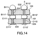
- the condition of the connection is shown in Figures 13 and 14.
- FIG. 13 is a perspective view of a J-part of FIG. 11 to an enlarged scale
- FIG. 14 is a sectional view taken along line G - G of FIG. 11.
- the through electrode pads B111 and B111', B112 and B112', C111 and C111', C112 and C112' are respectively connected to each other by through-hole internal electrodes S31, S32, S33, S34.
- the conductive bumps 6, as shown in FIG. 13, directly connect the electrode pads 111', 112' on the back side of the upper substrate 100 to the electrode pads 141, 142 on the surface side of the lower substrate 101 to each other.
- the connection form of the other electrode pad part is also similar to Figures 13 and 14.
- the respective electrode pads of the substrates 100, 101 are directly connected to each other vertically through the conductive bumps 6.
- the semiconductor devices 3 and 4 are vertically direct-coupled to each other through the conductive bumps 6 to be connected, and mounted facedown on a motherboard not shown through the conductive bumps 5.
- connection for chip select is a wiring part between the RAS terminal of the semiconductor chip 3 and the electrode pads 111, 112, and between the RAS terminal of the semiconductor chip 3 and the electrode pads 141, 142 (through hole electrode pads B111, B112, C111, C112).
- the connection pattern for chip select differs with the substrates of the respective layers.
- a chip select signal is supplied to the electrode pad connected to the RAS of the semiconductor chip 3. At this time, the chip select signal is transmitted to the electrode pad 142, but this is not connected to the RAS, so that the semiconductor device 4 is not selected.
- a chip select signal is supplied to the electrode pad 111 connected to the RAS of the semiconductor chip 4.
- chip select is enabled by changing wiring for chip select at every stage of the substrates. Hence it is necessary to use different substrates in the respective layers in the stacked module.
- a stacked module of the present invention is a stacked module constructed so that substrates on which a semiconductor device having a chip select terminal to be selected according to an external signal is mounted are stacked in N-layer (N is integers from 2 up) and the upper and lower terminals are connected to each other. All of the substrates (1, 2 in FIG. 3 and FIG. 6) have the same wiring structure.
- Each substrate (1 in FIG. 3 and FIG. 6) has N-number of chip select electrodes (B1 and 11, B2 and 12 in FIG. 3 and FIG. 6) arranged adjacent to each other, first chip select electrodes (B1 and 11, C1 and 41 in FIG. 3 and FIG. 6) among N-number of chip select electrodes are connected to the chip select terminal of a mounted semiconductor device (3 in FIG.
- substrates in common can be used all in N-number of layers so as to improve productivity, and even if the upper and lower positional relationship of the substrates is mistaken, there is no obstacle.
- the first chip select electrode is positioned at the most end of N-number of chip select electrodes.
- the other chip select electrodes and the opposite surface side electrodes positioned on the opposite surface side of the adjacent chip select electrode in the direction of the chip select electrode are, to be concrete, connected to each other by conductors (L1, S1, S2 in FIG. 3) arranged in the interior of the substrate.
- a stacked module in which first and second substrates are stacked and upper and lower terminals are connected to each other, is characterized in that the first and second substrates (1, 2 in FIG. 6) have the same wiring structure, the first substrate (1 in FIG. 6) has chip select electrodes (B1 and 11, B2 and 12) arranged adjacent to each other, one side chip select electrodes (B1 and 11) are connected to chip select terminals of a mounted semiconductor device (3 in FIG. 1), the other side chip select electrodes (B2, 12 and S10 in FIG. 6) are pierced through the first substrate to reach the opposite surface side and then connected to the opposite surface side electrodes (11' in FIG.
- the substrate of the present invention includes N-number (N is integers from 2 up) of chip select electrodes arranged adjacent to each other, wherein a first chip select electrode positioned at the most end of the N-number of chip select electrodes is connected to the chip select terminal of the semiconductor device, and the other chip select electrode is connected to the opposite surface side electrode positioned on the opposite surface side of the adjacent chip select electrode in the direction of the first chip select electrode.
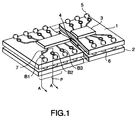
- FIG. 1 is a perspective view, with portions broken away, showing a first embodiment of a stacked module according to the present invention.
- the stacked module of FIG. 1 is equivalent to a memory circuit.
- semiconductor chips 3, 4 are respectively DRAM chips of DRAM 80, 81 of FIG. 10.
- the semiconductor chips 3, 4 are mounted facedown on substrates 1, 2.
- the matrices of the substrates 1, 2 are formed by an insulator such as ceramics or glass.
- a conductive bump 5 such as a solder bump is formed on each electrode pad of the substrate 1
- a conductive bump 6 such as a solder bump or the like is formed on each electrode pad of the substrate 2, and connection between the substrates is performed through the conductive bump 6.
- the conductive bump 5 serves as an external terminal at the time of mounting the stacked module of FIG. 1 facedown on a motherboard not shown.
- the number of external terminals is twenty four.
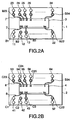
- FIG. 2A shows the upper substrate 1 on which the semiconductor chip 3 is mounted
- FIG. 2B shows the lower substrate 2 on which the semiconductor chip 4 is mounted
- they are plan views respectively showing the condition before the conductive bumps 5, 6 are mounted.
- the substrates 1 and 2 have the same wiring structure.
- FIG. 2A on the surface of the substrate 1, formed are 24 electrode pads 11 to 34 connected to the terminal (not shown) of the semiconductor chip 3, on which the conductive bump 5 of FIG. 1 is mounted, chip select electrode pads B1, B2 connected to the electrode pads 11, 12, through-hole electrode pads B3 to B34 connected to the electrode pads 13 to 34, and wirings 7 for connecting the chip select electrode pads B1, B2, and the through-hole electrode pads B3 to B34 to the respective terminals of the semiconductor chip 3.
- FIG. 2B on the surface of the substrate 2, formed are 24 electrode pads 41 to 64 connected to the terminal (not shown) of the semiconductor chip 4, on which the conductive bump 6 of FIG. 1 is mounted, chip select electrode pads C1, C2 connected to the electrode pads 41, 42, through-hole electrode pads C3 to C34 connected to the electrode pads 43 to 64, and wirings 8 for connecting the chip select electrode pads C1, C2 and the respective through-hole electrode pads to the respective terminals of the semiconductor chip 4.
- the electrode pads 11, 12 (B1, B2) and the electrode pads 41, 42 (C1, C2) of the substrates 1, 2 are the electrode pads for chip select of the semiconductor chips 3, 4, and the other electrode pads 13 to 34 and electrode pads 43 to 64 are connected to terminals other than the chip select terminals and also connected to each other at the time of stacking and packaging.
- the electrode pad 12 (B2) is not connected to the semiconductor chip 3, and the electrode pad 42 (C2) is not connected to the semiconductor chip 4.
- electrode pads for placing the conductive bumps 5, 6 thereon are provided separately from the conductive pads B1 to B34, C1 to C34 is to improve placing of the conductive bumps such as solder bumps or the like.
- the through-hole electrode pads B3 to B34 and the through-hole electrode pads C3 to C34 are electrically connected to through-hole electrode pads B3' to B34' and C3' to C34' (only reference numerals, not shown) formed on the back sides of the substrates 1, 2 through through-holes. Further, the same electrode pads 11' to 34' and 41' to 64' (only reference numerals, not shown) are formed on the back sides of the substrates 1, 2 of the electrode pads 11 to 34 and 41 to 64 on which the conductive bumps 5, 6 are placed.
- the electrode pads 11' to 34' on the back side of the substrate 1 are respectively connected to the chip select electrode pads B1', B2' and the through-hole electrode pads B31' to B34' on the same back side similarly to the surface side, and also the electrode pads 41' to 64' on the back side of the substrate 2 are respectively connected to the chip select electrode pads C1', C2' and the through-hole electrode pads C3' to C34' on the same back side.
- the electrode pads and the through-hole electrodes are formed in pair on the surface sides and the back sides of the substrates 1, 2, whereby the substrates may be used in any layer of the stacked module.
- the conductive bumps 6 respectively connect the electrode pads 41 to 64 of the surface side of the lower substrate 2 and the electrode pads 11' to 34' of the back side of the upper substrate 1 directly to each other. Thus, the connection between the semiconductor chips 3 and 4 through the conductive bumps 6 is enabled.
- FIG. 3 is a perspective view of a part P in FIG. 1 to an enlarged scale
- FIG. 4 is a sectional view taken along line A - A of FIG. 1.
- the chip select electrode pad B2 of the substrate 1 and the electrode pad B1' on the back side of the adjacent chip select electrode pad B1 are connected to each other inside the substrate 1
- the chip select electrode pad C2 of the substrate 2 and the electrode pad C1' on the back side of the adjacent chip select electrode pad C1 are connected to each other inside the substrate 2.
- the chip select electrode pad B2 is connected to the back side electrode pad B1' through a via hole internal electrode S2, an internal conductive layer L1, and a via hole internal electrode S1, and further connected from the electrode pad 11' through the conductive bump 6 to the chip select electrode pad C1.
- the chip select electrode pad C1 is connected to the RAS terminal of the semiconductor device 4 mounted on the lower substrate 2, so that a chip select signal supplied to the chip select electrode pad B2 is supplied to the terminal of RAS of the semiconductor chip 4 to be selected.
- the chip select electrode pad B1 is independent of the electrode pad B2.
- the electrode pad 11 (and B1) of the upper substrate 1 serving as a connecting terminal to a motherboard is connected to the RAS terminal of the semiconductor chip 3, so that chip select for the semiconductor chip 3 is performed by the electrode pad 11.
- chip select electrode pads B1 and B2 are utilized as a terminal for performing chip select for the semiconductor chips 3, 4.
- the same wiring structure as that of the substrate 1 is formed also in the inside of the substrate 2. That is, the chip select electrode C2 is connected to the electrode pad C1' and the electrode pad 41' on the back side through a via hole internal electrode S4, an internal conductive layer L2, and a via hole internal electrode S3.
- the chip select electrode pad C1 is independent of the electrode pad C2.
- the internal wiring of substrate 2 and the electrode pad C2 are unused wiring.
- the substrate 1 includes a two-layer structure of a first layer 1A and a second layer 1B.
- a via hole internal electrode S2 is formed
- a via hole internal electrode S1 is formed, and further an internal conductive layer L1 is formed.
- the substrate 2 is also obtained by forming a first layer 2A and a second layer 2B and stacking the same to each other by the same method as the substrate 1.
- the substrates 1 and 2 have the quite same wiring structure, so that the productivity is high and the yield is improved. Further, even if the positions of the substrates 1, 2 are inverted, the function will not be changed. Hence, it is not necessary to replace a stacked module so as to improve the economical efficiency.
- FIG. 5 is a sectional view showing a second embodiment in which a three-layer substrate is used. However, FIG. 5 shows a section of only a chip select electrode pad part. The wiring structure of the other electrode pads is approximately the same as that in the first embodiment, so the illustration and description are omitted.
- Chip select electrode pads B1 to B3, C1 to C3, D1 to D3 are formed on the surfaces of the substrates 100, 1001, 1002. Further on the back sides thereof, electrode pads B1' to B3', C1' to C3', D1' to D3' are similarly formed.
- the chip select electrode pads B1, C1, and D1 positioned at the most end (left end) are connected to the chip select terminals (RAS terminal of DRAM chip) of the semiconductor chips of the respective layers.
- Conductive bumps 5, 6, 6K are formed on separate electrode pads connected to the electrode pads B1 to B3, C1 to C3, D1 to D3 similarly to the first embodiment.
- the chip select electrode pads B2 and C1 are connected to each other through an internal conductive layer L1, via hole internal electrodes at both ends thereof, and a conductive bump 6, and the chip select electrode pads B3 and D1 are connected to each other through an internal conductive layer L4, via hole internal electrodes at both ends thereof, a conductive bump 6, an electrode pad C2, an internal conductive layer L2 and a conductive bump 6K.
- the respective internal conductive layers L1 to L6 are extended independently of each other toward the chip select electrode pads C1, D1 connected to the chip select terminal (RAS terminal of DRAM chip) of the semiconductor chip.
- the chip select electrode pads B1, B2 and B3 are individually connected to the chip select terminal (RAS terminal) of the semiconductor chip of the substrate of each layer. Moreover, the wiring structure is the same in the respective substrates.
- the internal conductive layers L3, L5, L6 are not used in the case of FIG: 5.
- the substrate is two-layer or three-layer, but in the case of performing chip select for N-number (N is integers) of semiconductor chips, a substrate of N-layer structure is used.
- the number of chip select electrode pads is N equal to that of the semiconductor chips, the respective chip select electrode pads are connected through internal wiring of the substrate and conductive bumps between the upper and lower substrates to the chip select terminal (e.g. RAS terminal of DRAM) of one semiconductor chip to be selected.
- electrodes electrode pads and through-hole internal electrodes vertically piercing the substrates to be connected to each other and N-number of chip select electrode pads are formed on the surfaces of the respective substrates.
- a first chip select electrode pad on the surface of the substrate of the i-th layer (1 ⁇ i ⁇ N, i is integers) from above is connected to a second chip select electrode pad positioned on the opposite surface side of the adjacent chip select electrode pad.
- This connection is performed through an internal conductor (conductive layer).
- the internal conductor is formed toward the direction in which the chip select electrode pad (first chip select electrode pad) connected to the chip select terminal of the semiconductor device is positioned.
- the second chip select electrode pad is connected to a chip select electrode pad on the surface of the substrate of the (i+1)-th layer from above through a conductive bump.
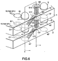
- FIG. 6 is a partial perspective view showing a third embodiment of a stacked module according to the present invention
- FIG. 7 is a sectional view taken along line C - C of FIG. 6.
- back conductive layers L10, L11 are formed on the back sides of the substrates 1, 2 instead of the internal conductive layers L1 and L2 in the embodiment shown in Figures 3 and 4.
- No through-hole and via hole are not formed between the chip select electrode pad B1 (C1) and the electrode pad B1' (C1') on the back side thereof.
- the electrode pads B1' and 11', B2' and 12', C1' and 41', C2' and 42' are not connected with each other.
- the chip select electrode pad B1 is connected to the chip select terminal of the semiconductor chip of the substrate 1.
- the chip select electrode pad B2 is connected through the through-hole internal electrode S10 to the electrode pad B2' on the back side.
- the electrode pad B2' is further connected to the chip select terminal of the semiconductor chip of the substrate 2 through a back conductive layer L10, the back electrode pad 11', the conductive bump 6 and the chip select electrode pad C1.
- the chip select electrode pads B1, B2 function as chip select external terminals of two semiconductor chips similarly to the first embodiment.
- the chip select electrode pad C2 of the substrate 2 is connected through a through-hole internal electrode S11 to an electrode pad C2' on the back side, and further connected from the back conductive layer L11 to the back electrode pad 41', but this connecting path is not used for chip select.
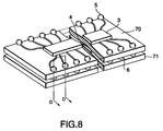
- FIG. 8 is a perspective view showing a fourth embodiment of a stacked module according to the present invention
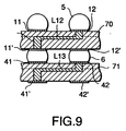
- FIG. 9 is a sectional view taken along line D - D of FIG. 8.
- the stacked module shown in FIG. 8 is so constructed that the same functions as those of the electrode pads B1 to B34 and C1 to C34 shown in FIG. 1 are joined with the electrode pads where the conductive bumps 5, 6 are formed.
- electrode pads 11, 12 on the surface of a substrate 70 on which a semiconductor chip 3 is mounted, and electrode pads 41, 42 on the surface of a substrate 71 on which a semiconductor chip 4 is mounted are chip select electrode pads.
- the other electrode pads are vertically connected to each other through a conductor piercing through the substrates 70, 71.
- the internal conductors L12, L13 play a part instead of the internal conductive layers L1, L2 of FIG. 4.
- connection between the chip select electrode pad and the internal conductive layer is performed by the via hole internal electrode, but in FIG. 9, the via hole is filled up with internal conductors L12, L13.
- no holes such as a via hole and a through-hole are formed in the electrode pads where the conductive bumps 5, 6 are formed, so that the conductive bumps 5, 6 can be formed directly on the electrode pad surface so as to reduce the number of the electrode pads.
- a semiconductor device mounted on a substrate is not limited to a base chip of a semiconductor, but it may be a semiconductor package packaged by resin or ceramics.
- the semiconductor chip 3 is mounted on a surface where the conductive bump 5 is formed in FIG. 1, the semiconductor chip 3 may be mounted on the opposite side to the surface. Further, the chip select electrode pads may be positioned in any place if only they are adjacent to each other. For example, the chip select electrode pads may be formed in the positions of the electrode pads B3, B4.
- first chip select electrodes e.g. B1 and 11, C1 and 42
- the other chip select electrodes B2 and 12 in FIG. 3
- the opposite surface side electrodes B1' and 11' in FIG. 3
- the opposite surface side electrodes and the chip select electrodes (C1 and 41 in FIG. 3) of the substrate (2 in FIG. 3) confronting therewith are connected to each other by the conductive bump (6 in FIG. 3).
- the chip select electrode may be an electrode pad or an electrode pin.
- a conductive bump is not needed.
- a conductive line other than the electrode pin may be all right.
- the other chip select electrodes and the opposite surface side electrodes positioned on the opposite surface side of the adjacent chip select electrode in the direction of the chip select electrode are connected to each other by conductors (e.g. L1, S1, S2 in FIG. 3) arranged in the interior of the substrate.
- the conductors may have any shape.
- the productivity is high and the yield can be improved. Furthermore, even if the positions of the substrates 1, 2 are inverted, the function will not be changed, so that it is not necessary to replace a stacked module and the economical efficiency can be improved.
Landscapes
- Engineering & Computer Science (AREA)
- Microelectronics & Electronic Packaging (AREA)
- Dram (AREA)
- Combinations Of Printed Boards (AREA)
- Production Of Multi-Layered Print Wiring Board (AREA)
- Internal Circuitry In Semiconductor Integrated Circuit Devices (AREA)
- Wire Bonding (AREA)
Applications Claiming Priority (3)
| Application Number | Priority Date | Filing Date | Title |
|---|---|---|---|
| JP9298909A JP2870530B1 (ja) | 1997-10-30 | 1997-10-30 | スタックモジュール用インターポーザとスタックモジュール |
| JP29890997 | 1997-10-30 | ||
| JP298909/97 | 1997-10-30 |
Publications (2)
| Publication Number | Publication Date |
|---|---|
| EP0915516A2 true EP0915516A2 (fr) | 1999-05-12 |
| EP0915516A3 EP0915516A3 (fr) | 2004-01-02 |
Family
ID=17865748
Family Applications (1)
| Application Number | Title | Priority Date | Filing Date |
|---|---|---|---|
| EP98120397A Withdrawn EP0915516A3 (fr) | 1997-10-30 | 1998-10-28 | Substrat pour module empilé et module empilé |
Country Status (5)
| Country | Link |
|---|---|
| US (1) | US5995379A (fr) |
| EP (1) | EP0915516A3 (fr) |
| JP (1) | JP2870530B1 (fr) |
| KR (1) | KR100298282B1 (fr) |
| TW (1) | TW405247B (fr) |
Cited By (4)
| Publication number | Priority date | Publication date | Assignee | Title |
|---|---|---|---|---|
| DE10049551A1 (de) * | 1999-10-26 | 2001-05-03 | Sharp Kk | Gestapeltes Halbleiterbauteil |
| DE10134648A1 (de) * | 2001-07-20 | 2002-10-10 | Infineon Technologies Ag | Anordnung aus gestapelten elektronischen Bauteilen und Verfahren zur Herstellung der Anordnung |
| EP1288968A2 (fr) * | 2001-07-24 | 2003-03-05 | Hewlett-Packard Company | Méoire à l'étât solide |
| EP1685600A4 (fr) * | 2003-09-05 | 2008-05-14 | Sanmina Sci Corp | Ensemble electronique empilable |
Families Citing this family (75)
| Publication number | Priority date | Publication date | Assignee | Title |
|---|---|---|---|---|
| US6002177A (en) * | 1995-12-27 | 1999-12-14 | International Business Machines Corporation | High density integrated circuit packaging with chip stacking and via interconnections |
| JP3268740B2 (ja) | 1997-08-20 | 2002-03-25 | 株式会社東芝 | Asicの設計製造方法、スタンダードセル、エンベッテドアレイ、及びマルチ・チップ・パッケージ |
| JP3727172B2 (ja) * | 1998-06-09 | 2005-12-14 | 沖電気工業株式会社 | 半導体装置 |
| JP3563604B2 (ja) * | 1998-07-29 | 2004-09-08 | 株式会社東芝 | マルチチップ半導体装置及びメモリカード |
| US6504241B1 (en) * | 1998-10-15 | 2003-01-07 | Sony Corporation | Stackable semiconductor device and method for manufacturing the same |
| US6122187A (en) * | 1998-11-23 | 2000-09-19 | Micron Technology, Inc. | Stacked integrated circuits |
| KR100319608B1 (ko) * | 1999-03-09 | 2002-01-05 | 김영환 | 적층형 반도체 패키지 및 그 제조방법 |
| JP2000277944A (ja) * | 1999-03-24 | 2000-10-06 | Ando Electric Co Ltd | 増設用の基板および基板の増設方法 |
| JP3213292B2 (ja) * | 1999-07-12 | 2001-10-02 | ソニーケミカル株式会社 | 多層基板、及びモジュール |
| US6521483B1 (en) | 1999-07-22 | 2003-02-18 | Seiko Epson Corporation | Semiconductor device, method of manufacture thereof, circuit board, and electronic device |
| KR100343453B1 (ko) * | 1999-10-28 | 2002-07-11 | 박종섭 | 다중 적층형 메모리 모듈 |
| US6404660B1 (en) | 1999-12-23 | 2002-06-11 | Rambus, Inc. | Semiconductor package with a controlled impedance bus and method of forming same |
| DE10009171B4 (de) * | 2000-02-26 | 2005-08-11 | Robert Bosch Gmbh | Stromrichter und sein Herstellverfahren |
| JP3779524B2 (ja) * | 2000-04-20 | 2006-05-31 | 株式会社東芝 | マルチチップ半導体装置及びメモリカード |
| DE10044148A1 (de) * | 2000-09-06 | 2002-03-21 | Infineon Technologies Ag | Elektronisches Bauteil mit gestapelten Bausteinen und Verfahren zu seiner Herstellung |
| JP3405456B2 (ja) * | 2000-09-11 | 2003-05-12 | 沖電気工業株式会社 | 半導体装置,半導体装置の製造方法,スタック型半導体装置及びスタック型半導体装置の製造方法 |
| US7240254B2 (en) * | 2000-09-21 | 2007-07-03 | Inapac Technology, Inc | Multiple power levels for a chip within a multi-chip semiconductor package |
| US6812726B1 (en) * | 2002-11-27 | 2004-11-02 | Inapac Technology, Inc. | Entering test mode and accessing of a packaged semiconductor device |
| US7444575B2 (en) * | 2000-09-21 | 2008-10-28 | Inapac Technology, Inc. | Architecture and method for testing of an integrated circuit device |
| JP3934867B2 (ja) * | 2000-09-29 | 2007-06-20 | 株式会社東芝 | 不揮発性半導体記憶装置および不揮発性半導体メモリシステム |
| US6653572B2 (en) * | 2001-02-07 | 2003-11-25 | The Furukawa Electric Co., Ltd. | Multilayer circuit board |
| KR100364635B1 (ko) * | 2001-02-09 | 2002-12-16 | 삼성전자 주식회사 | 칩-레벨에 형성된 칩 선택용 패드를 포함하는 칩-레벨3차원 멀티-칩 패키지 및 그 제조 방법 |
| US7610447B2 (en) * | 2001-02-28 | 2009-10-27 | Rambus Inc. | Upgradable memory system with reconfigurable interconnect |
| US6889304B2 (en) | 2001-02-28 | 2005-05-03 | Rambus Inc. | Memory device supporting a dynamically configurable core organization |
| US6469375B2 (en) * | 2001-02-28 | 2002-10-22 | William F. Beausoleil | High bandwidth 3D memory packaging technique |
| DE10125025A1 (de) * | 2001-05-22 | 2002-12-12 | Infineon Technologies Ag | Schaltungsplantine für Speicherbauelemente |
| JP4109839B2 (ja) * | 2001-06-01 | 2008-07-02 | 株式会社東芝 | 半導体装置 |
| US6914786B1 (en) * | 2001-06-14 | 2005-07-05 | Lsi Logic Corporation | Converter device |
| JP2003060053A (ja) * | 2001-08-10 | 2003-02-28 | Fujitsu Ltd | 半導体チップ及びそれを用いた半導体集積回路装置及び半導体チップ選択方法 |
| JP2003100947A (ja) | 2001-09-20 | 2003-04-04 | Mitsubishi Electric Corp | 半導体装置及び半導体装置モジュール |
| US8166361B2 (en) | 2001-09-28 | 2012-04-24 | Rambus Inc. | Integrated circuit testing module configured for set-up and hold time testing |
| US8286046B2 (en) | 2001-09-28 | 2012-10-09 | Rambus Inc. | Integrated circuit testing module including signal shaping interface |
| US7313740B2 (en) * | 2002-07-25 | 2007-12-25 | Inapac Technology, Inc. | Internally generating patterns for testing in an integrated circuit device |
| US8001439B2 (en) | 2001-09-28 | 2011-08-16 | Rambus Inc. | Integrated circuit testing module including signal shaping interface |
| US6611052B2 (en) * | 2001-11-16 | 2003-08-26 | Micron Technology, Inc. | Wafer level stackable semiconductor package |
| US7046522B2 (en) * | 2002-03-21 | 2006-05-16 | Raymond Jit-Hung Sung | Method for scalable architectures in stackable three-dimensional integrated circuits and electronics |
| US6542393B1 (en) | 2002-04-24 | 2003-04-01 | Ma Laboratories, Inc. | Dual-bank memory module with stacked DRAM chips having a concave-shaped re-route PCB in-between |
| US6891447B2 (en) * | 2002-07-12 | 2005-05-10 | Massachusetts Institute Of Technology | Electromagnetic coupling connector for three-dimensional electronic circuits |
| US8063650B2 (en) | 2002-11-27 | 2011-11-22 | Rambus Inc. | Testing fuse configurations in semiconductor devices |
| US6809269B2 (en) * | 2002-12-19 | 2004-10-26 | Endicott Interconnect Technologies, Inc. | Circuitized substrate assembly and method of making same |
| US7183643B2 (en) * | 2003-11-04 | 2007-02-27 | Tessera, Inc. | Stacked packages and systems incorporating the same |
| TW200535918A (en) * | 2004-03-09 | 2005-11-01 | Japan Science & Tech Agency | Semiconductor device and methods for fabricating the same, semiconductor system having laminated structure, semiconductor interposer, and semiconductor system |
| US20060206745A1 (en) * | 2005-03-11 | 2006-09-14 | Advanced Micro Devices, Inc. | Automatic resource assignment in devices having stacked modules |
| US7251160B2 (en) * | 2005-03-16 | 2007-07-31 | Sandisk Corporation | Non-volatile memory and method with power-saving read and program-verify operations |
| JP4577688B2 (ja) | 2005-05-09 | 2010-11-10 | エルピーダメモリ株式会社 | 半導体チップ選択方法、半導体チップ及び半導体集積回路装置 |
| US7095602B1 (en) | 2005-06-29 | 2006-08-22 | Murata Manufacturing Co., Ltd. | Ceramic structure and nonreciprocal circuit device |
| US7826243B2 (en) * | 2005-12-29 | 2010-11-02 | Bitmicro Networks, Inc. | Multiple chip module and package stacking for storage devices |
| JP4753725B2 (ja) * | 2006-01-20 | 2011-08-24 | エルピーダメモリ株式会社 | 積層型半導体装置 |
| US7701045B2 (en) * | 2006-04-11 | 2010-04-20 | Rambus Inc. | Point-to-point connection topology for stacked devices |
| US7506098B2 (en) * | 2006-06-08 | 2009-03-17 | Bitmicro Networks, Inc. | Optimized placement policy for solid state storage devices |
| US7952184B2 (en) | 2006-08-31 | 2011-05-31 | Micron Technology, Inc. | Distributed semiconductor device methods, apparatus, and systems |
| KR100827724B1 (ko) | 2006-09-12 | 2008-05-07 | 엠텍비젼 주식회사 | 웨이퍼 레벨 패키지 적층 구조를 가지는 시스템 인 패키지및 그 제조 방법 |
| US7781927B2 (en) * | 2006-10-13 | 2010-08-24 | Lg Innotek Co., Ltd. | Vibration motor |
| US7754532B2 (en) | 2006-10-19 | 2010-07-13 | Micron Technology, Inc. | High density chip packages, methods of forming, and systems including same |
| US7605477B2 (en) * | 2007-01-25 | 2009-10-20 | Raytheon Company | Stacked integrated circuit assembly |
| KR100874926B1 (ko) * | 2007-06-07 | 2008-12-19 | 삼성전자주식회사 | 스택 모듈, 이를 포함하는 카드 및 이를 포함하는 시스템 |
| US8078339B2 (en) * | 2007-07-13 | 2011-12-13 | Cummins Inc. | Circuit board with integrated connector |
| US8560124B2 (en) | 2007-07-13 | 2013-10-15 | Cummins Inc. | Idle control system and method for adaptive temperature control |
| KR101176187B1 (ko) * | 2007-11-21 | 2012-08-22 | 삼성전자주식회사 | 스택형 반도체 장치 및 이 장치의 직렬 경로 형성 방법 |
| JP2009239256A (ja) * | 2008-03-03 | 2009-10-15 | Panasonic Corp | 半導体装置及びその製造方法 |
| US8082537B1 (en) | 2009-01-28 | 2011-12-20 | Xilinx, Inc. | Method and apparatus for implementing spatially programmable through die vias in an integrated circuit |
| US7989959B1 (en) * | 2009-01-29 | 2011-08-02 | Xilinx, Inc. | Method of forming stacked-die integrated circuit |
| US8987868B1 (en) | 2009-02-24 | 2015-03-24 | Xilinx, Inc. | Method and apparatus for programmable heterogeneous integration of stacked semiconductor die |
| KR20100096879A (ko) * | 2009-02-25 | 2010-09-02 | 삼성전자주식회사 | 구리 패드를 포함하는 반도체 소자, 그 적층 구조 및 그 제조 방법 |
| CN101894829B (zh) * | 2009-05-19 | 2012-06-27 | 国碁电子(中山)有限公司 | 堆叠式封装结构 |
| KR20110112707A (ko) | 2010-04-07 | 2011-10-13 | 삼성전자주식회사 | 층간 연결 유닛을 갖는 적층 메모리 장치, 이를 포함하는 메모리 시스템, 및 전송선의 지연시간 보상 방법 |
| US9015023B2 (en) | 2010-05-05 | 2015-04-21 | Xilinx, Inc. | Device specific configuration of operating voltage |
| US9000490B2 (en) | 2013-04-19 | 2015-04-07 | Xilinx, Inc. | Semiconductor package having IC dice and voltage tuners |
| KR102077608B1 (ko) * | 2013-09-26 | 2020-02-17 | 에스케이하이닉스 주식회사 | 반도체 칩 및 이를 갖는 스택 패키지 |
| US9893037B1 (en) * | 2017-04-20 | 2018-02-13 | Nanya Technology Corporation | Multi-chip semiconductor package, vertically-stacked devices and manufacturing thereof |
| JP2020145351A (ja) * | 2019-03-07 | 2020-09-10 | キオクシア株式会社 | 半導体装置およびその製造方法 |
| US11004833B1 (en) * | 2020-02-17 | 2021-05-11 | Xilinx, Inc. | Multi-chip stacked devices |
| KR102714883B1 (ko) * | 2020-06-25 | 2024-10-07 | 삼성전자주식회사 | 반도체 패키지 |
| US12015003B2 (en) | 2021-09-29 | 2024-06-18 | International Business Machines Corporation | High density interconnection and wiring layers, package structures, and integration methods |
| US12170252B2 (en) | 2021-09-29 | 2024-12-17 | International Business Machines Corporation | Electronic substrate stacking |
Family Cites Families (12)
| Publication number | Priority date | Publication date | Assignee | Title |
|---|---|---|---|---|
| JPS6129140A (ja) * | 1984-07-20 | 1986-02-10 | Hitachi Ltd | 半導体装置 |
| US5198888A (en) * | 1987-12-28 | 1993-03-30 | Hitachi, Ltd. | Semiconductor stacked device |
| JPH03295266A (ja) * | 1990-04-12 | 1991-12-26 | Hitachi Ltd | 高集積半導体装置 |
| US5130894A (en) * | 1990-11-26 | 1992-07-14 | At&T Bell Laboratories | Three-dimensional circuit modules |
| JPH0513666A (ja) * | 1991-06-29 | 1993-01-22 | Sony Corp | 複合半導体装置 |
| US5397916A (en) * | 1991-12-10 | 1995-03-14 | Normington; Peter J. C. | Semiconductor device including stacked die |
| US5434452A (en) * | 1993-11-01 | 1995-07-18 | Motorola, Inc. | Z-axis compliant mechanical IC wiring substrate and method for making the same |
| US5585675A (en) * | 1994-05-11 | 1996-12-17 | Harris Corporation | Semiconductor die packaging tub having angularly offset pad-to-pad via structure configured to allow three-dimensional stacking and electrical interconnections among multiple identical tubs |
| US5434745A (en) * | 1994-07-26 | 1995-07-18 | White Microelectronics Div. Of Bowmar Instrument Corp. | Stacked silicon die carrier assembly |
| JP2944449B2 (ja) * | 1995-02-24 | 1999-09-06 | 日本電気株式会社 | 半導体パッケージとその製造方法 |
| US5612570A (en) * | 1995-04-13 | 1997-03-18 | Dense-Pac Microsystems, Inc. | Chip stack and method of making same |
| US5854507A (en) * | 1998-07-21 | 1998-12-29 | Hewlett-Packard Company | Multiple chip assembly |
-
1997
- 1997-10-30 JP JP9298909A patent/JP2870530B1/ja not_active Expired - Lifetime
-
1998
- 1998-10-19 TW TW087117285A patent/TW405247B/zh not_active IP Right Cessation
- 1998-10-23 US US09/177,384 patent/US5995379A/en not_active Expired - Lifetime
- 1998-10-28 EP EP98120397A patent/EP0915516A3/fr not_active Withdrawn
- 1998-10-29 KR KR19980045750A patent/KR100298282B1/ko not_active Expired - Lifetime
Cited By (6)
| Publication number | Priority date | Publication date | Assignee | Title |
|---|---|---|---|---|
| DE10049551A1 (de) * | 1999-10-26 | 2001-05-03 | Sharp Kk | Gestapeltes Halbleiterbauteil |
| US6362529B1 (en) | 1999-10-26 | 2002-03-26 | Sharp Kabushiki Kaisha | Stacked semiconductor device |
| KR100414839B1 (ko) * | 1999-10-26 | 2004-01-13 | 샤프 가부시키가이샤 | 적층형 반도체 장치 |
| DE10134648A1 (de) * | 2001-07-20 | 2002-10-10 | Infineon Technologies Ag | Anordnung aus gestapelten elektronischen Bauteilen und Verfahren zur Herstellung der Anordnung |
| EP1288968A2 (fr) * | 2001-07-24 | 2003-03-05 | Hewlett-Packard Company | Méoire à l'étât solide |
| EP1685600A4 (fr) * | 2003-09-05 | 2008-05-14 | Sanmina Sci Corp | Ensemble electronique empilable |
Also Published As
| Publication number | Publication date |
|---|---|
| JP2870530B1 (ja) | 1999-03-17 |
| TW405247B (en) | 2000-09-11 |
| EP0915516A3 (fr) | 2004-01-02 |
| JPH11135711A (ja) | 1999-05-21 |
| KR100298282B1 (ko) | 2001-09-06 |
| KR19990037491A (ko) | 1999-05-25 |
| US5995379A (en) | 1999-11-30 |
Similar Documents
| Publication | Publication Date | Title |
|---|---|---|
| US5995379A (en) | Stacked module and substrate therefore | |
| US4956694A (en) | Integrated circuit chip stacking | |
| KR100293775B1 (ko) | 3차원 메모리모듈 및 이를 이용한 반도체장치 | |
| US5780925A (en) | Lead frame package for electronic devices | |
| USRE36916E (en) | Apparatus for stacking semiconductor chips | |
| US5396102A (en) | Semiconductor device | |
| US7183643B2 (en) | Stacked packages and systems incorporating the same | |
| US9355996B2 (en) | Microelectronic package with consolidated chip structures | |
| US8344518B2 (en) | Apparatus for stacking integrated circuits | |
| US4984064A (en) | Semiconductor device | |
| CN1951161B (zh) | 区域阵列零件的共用通路退耦 | |
| US6011695A (en) | External bus interface printed circuit board routing for a ball grid array integrated circuit package | |
| US7095107B2 (en) | Ball assignment schemes for integrated circuit packages | |
| US6770980B2 (en) | Semiconductor device having semiconductor element packaged on interposer | |
| US5691569A (en) | Integrated circuit package that has a plurality of staggered pins | |
| US20060202317A1 (en) | Method for MCP packaging for balanced performance | |
| JPH0239101B2 (fr) | ||
| US20030067082A1 (en) | Apparatus and methods for stacking integrated circuit devices with interconnected stacking structure | |
| US6295220B1 (en) | Memory bar and related circuits and methods | |
| JPH09186424A (ja) | プリント回路基板 | |
| US6188133B1 (en) | Semiconductor with plurality of connecting parts arranged on lower surface of a substrate | |
| JP2515755B2 (ja) | 半導体装置 | |
| JPH10242190A (ja) | メモリモジュール | |
| JP2664720B2 (ja) | Ic実装装置 | |
| KR20020041114A (ko) | 반도체 칩 및 그를 이용한 반도체 칩 패키지 |
Legal Events
| Date | Code | Title | Description |
|---|---|---|---|
| PUAI | Public reference made under article 153(3) epc to a published international application that has entered the european phase |
Free format text: ORIGINAL CODE: 0009012 |
|
| AK | Designated contracting states |
Kind code of ref document: A2 Designated state(s): AT BE CH CY DE DK ES FI FR GB GR IE IT LI LU MC NL PT SE |
|
| AX | Request for extension of the european patent |
Free format text: AL;LT;LV;MK;RO;SI |
|
| PUAL | Search report despatched |
Free format text: ORIGINAL CODE: 0009013 |
|
| AK | Designated contracting states |
Kind code of ref document: A3 Designated state(s): AT BE CH CY DE DK ES FI FR GB GR IE IT LI LU MC NL PT SE |
|
| AX | Request for extension of the european patent |
Extension state: AL LT LV MK RO SI |
|
| 17P | Request for examination filed |
Effective date: 20031118 |
|
| AKX | Designation fees paid |
Designated state(s): DE FR GB |
|
| 17Q | First examination report despatched |
Effective date: 20050415 |
|
| STAA | Information on the status of an ep patent application or granted ep patent |
Free format text: STATUS: THE APPLICATION IS DEEMED TO BE WITHDRAWN |
|
| 18D | Application deemed to be withdrawn |
Effective date: 20050826 |