EP0916450B1 - Verfahren und Vorrichtung zum Polieren von Halbleiterscheiben - Google Patents
Verfahren und Vorrichtung zum Polieren von Halbleiterscheiben Download PDFInfo
- Publication number
- EP0916450B1 EP0916450B1 EP98119004A EP98119004A EP0916450B1 EP 0916450 B1 EP0916450 B1 EP 0916450B1 EP 98119004 A EP98119004 A EP 98119004A EP 98119004 A EP98119004 A EP 98119004A EP 0916450 B1 EP0916450 B1 EP 0916450B1
- Authority
- EP
- European Patent Office
- Prior art keywords
- polishing
- semiconductor wafers
- regions
- temperatures
- plate
- Prior art date
- Legal status (The legal status is an assumption and is not a legal conclusion. Google has not performed a legal analysis and makes no representation as to the accuracy of the status listed.)
- Expired - Lifetime
Links
Images
Classifications
-
- B—PERFORMING OPERATIONS; TRANSPORTING
- B24—GRINDING; POLISHING
- B24B—MACHINES, DEVICES, OR PROCESSES FOR GRINDING OR POLISHING; DRESSING OR CONDITIONING OF ABRADING SURFACES; FEEDING OF GRINDING, POLISHING, OR LAPPING AGENTS
- B24B37/00—Lapping machines or devices; Accessories
- B24B37/11—Lapping tools
- B24B37/12—Lapping plates for working plane surfaces
-
- B—PERFORMING OPERATIONS; TRANSPORTING
- B24—GRINDING; POLISHING
- B24B—MACHINES, DEVICES, OR PROCESSES FOR GRINDING OR POLISHING; DRESSING OR CONDITIONING OF ABRADING SURFACES; FEEDING OF GRINDING, POLISHING, OR LAPPING AGENTS
- B24B37/00—Lapping machines or devices; Accessories
- B24B37/005—Control means for lapping machines or devices
- B24B37/015—Temperature control
-
- B—PERFORMING OPERATIONS; TRANSPORTING
- B24—GRINDING; POLISHING
- B24B—MACHINES, DEVICES, OR PROCESSES FOR GRINDING OR POLISHING; DRESSING OR CONDITIONING OF ABRADING SURFACES; FEEDING OF GRINDING, POLISHING, OR LAPPING AGENTS
- B24B37/00—Lapping machines or devices; Accessories
- B24B37/04—Lapping machines or devices; Accessories designed for working plane surfaces
- B24B37/042—Lapping machines or devices; Accessories designed for working plane surfaces operating processes therefor
Definitions
- the invention relates to a method for polishing semiconductor wafers the at least one side of at least one semiconductor wafer against one with one Polishing cloth covered polishing plate is pressed and polished, the semiconductor wafer and the polishing plate perform a relative movement.
- planarization of a semiconductor wafer using a chemo-mechanical polishing process forms an important processing step in the manufacturing process a flat, defect-free and smooth semiconductor wafer.
- This polishing step sets in many manufacturing processes the last shaping and thus the surface properties significantly determining step before reusing the semiconductor wafer as a raw material for the manufacture of electrical, electronic and microelectronic Components represent.
- the objectives of the polishing process are in particular the achievement a high level of flatness and parallelism of the two disc sides, the removal through Pretreatment of damaged surface layers ("damage removal") and reduction the micro roughness of the semiconductor wafer.
- Single-sided and double-sided polishing processes are usually used.
- single side batch polishing the semiconductor wafers with one side on the front of a carrier plate mounted by a positive and non-positive between the side and the support plate Connection, for example by adhesion, gluing, kitten or vacuum application, will be produced.
- the semiconductor wafers are placed on the Carrier plate mounted so that they form a pattern of concentric rings.
- a polishing agent a polishing plate, over which a polishing cloth is stretched, with a certain polishing force pressed and polished.
- the carrier plate and the polishing plate are thereby usually rotated at different speeds.
- the necessary polishing force is provided by a pressure stamp hereinafter referred to as "polishing head” transfer the back of the carrier plate.
- a variety of used polishing machines are designed so that they over have several polishing pots and accordingly several carrier plates be able to record.
- Double side polishing With double side polishing (DSP) the front and back are polished simultaneously by several semiconductor wafers between two covered with polishing cloths, upper and lower polishing plates. there the semiconductor wafers lie in thin guide cages ("wafer carrier"), which are referred to as rotor disks and in a similar form when lapping semiconductor wafers be used. Double-sided polishing processes and devices are always for the treatment of groups of semiconductor wafers designed ("batch polishing").
- Polished semiconductor wafers often have pages that are not parallel to each other but in cross-section the shape of a wedge take in.
- the shape of the wedge can be described with the term linear thickness variation describe.
- the linear thickness variation is the largest measured difference in thickness between two measuring points, the on the same diameter symmetrical to the center of the semiconductor wafer lie.
- the measuring points are usually symmetrical on a circle that is a distance of, for example 6 mm from the edge of the wafer of the semiconductor wafer. Is the edge the semiconductor wafer, which faces the edge of the carrier plate, thicker (thinner) than the edge of the pane, towards the center of the carrier plate shows, one speaks of a positive (negative) linear Wedging.
- TTV total thickness variation
- the wedging of a semiconductor wafer caused by the polishing is the result an uneven material removal. It can arise if the carrier plate while the polish is deformed radially by its own weight or a certain radial wedge-shape due to manufacturing. Sometimes there is an emerging one Wear of the polishing cloth Cause that the disc geometry in the Several polishing runs deteriorated. A certain basic wedge results even when using ideally flat carrier plates due to the kinematic conditions for single disc polishing, which promote inhomogeneous material removal.
- EP-4033 A1 proposes intermediate layers made of soft elastic bodies between the polishing pot and the back of the carrier plate, whereby the carrier plate is intentionally curved a little radially symmetrically. With that, too to a certain extent be prevented that the semiconductor wafers are polished wedge-shaped.
- this method cannot be automated and is prone to errors because of its success largely depends on the experience and prudence of the operators that choose the intermediate layers based on their width and insert them. But also if no mistakes are made, the wedge of the polished semiconductor wafers remains above a certain limit.
- the present invention solves the problem of polishing semiconductor wafers to achieve improved uniformity of the polishing removal, so that in particular the wedge shape of the polished semiconductor wafers is low.
- the invention relates to a method for polishing semiconductor wafers the at least one side of at least one semiconductor wafer against one with one Polishing cloth covered polishing plate is pressed and polished, the semiconductor wafer and the polishing plate perform a relative movement, characterized in that the Semiconductor wafer during polishing at least two areas on the polishing plate sweeps that have certain radial latitudes and different temperatures and tempering agents are provided in the polishing plate, with the help of which the number, the radial latitudes and the temperatures of the areas before polishing the Semiconductor wafers can be set.
- a radially convex temperature profile arises during polishing on the polishing plate, which is used for the wedging of polished semiconductor wafers is jointly responsible.
- the temperature profile causes an inhomogeneous material removal, not by using the above-mentioned elastic intermediate layers (for example when using ceramic carrier plates that are practically not curved ) or not sufficient (when using carrier plates from less stiff material) can be compensated.
- the invention makes it possible to polish the wedge of Setting semiconductor wafers within comparatively wide limits. By the invention can produce semiconductor wafers that are specifically positive or negative wedge are.
- the invention is primarily used for kinematic influences and influences of the carrier plate or the polishing cloth, which too Wedges would lead to compensate and for example an extension of the service life of the polishing cloth to reach.
- the invention can be used both for one-sided polishing (one and Multi-disc polish), as well as for double-sided polish become.
- the invention is illustrated below using the example multi-disc single-side polishing (single-side batch polishing) explained in more detail.
- the semiconductor wafers at least two areas during polishing paint over the polishing plate, which is caused by temperature control in the Polishing pads are kept at certain temperatures.
- the Areas are preferably laid out in concentric rings, taking temperatures from at least two of the ranges differ.
- the number, the radial latitudes and the temperatures the areas are determined before a polishing run. Not excluded is the temperature at which the areas be held during a polishing run change.
- the polishing cloth wears during polishing Semiconductor wafers on a conventional polishing plate are not homogeneous Temperature before.
- the temperature often increases from the edge r / 2 of the polishing plate (r is the radius of the polishing plate) and falls off towards the center of the polishing plate, making a radial convex temperature profile results.
- r is the radius of the polishing plate
- a homogenization of the temperature profile can be achieved.
- a radially convex temperature profile should be at least two tempered areas can be set up on the polishing plate.
- radial temperature profile are made uniform.
- the number of areas, their radial latitude and the temperatures, on which they are held are before polishing of the semiconductor wafers.
- the basis for the determination can data from an analysis of the geometry previously polished Semiconductor wafers are used, for example the linear thickness variation determined for these semiconductor wafers. Measurement data of the radial temperature profile can also form the basis of the polishing plate during a previous one Polishing run were determined.
- the functional relationship between that after a polish too expected geometry of the semiconductor wafers and the one to be determined Number, width and temperatures of the areas on the The polishing plate is expediently carried out by routine experimentation determined. In such experiments, the number is radial Systematic changes in width and temperature of the areas and the effects on the geometry of the polished semiconductor wafers examined.
- the polishing process can be started be automated easily.
- a host computer dialed as input data the radial temperature profile, which during a previous polishing run or data on the geometry (for example on the wedge shape) of semiconductor wafers, which polishes on a walking polishing trip have been based on the empirical relationship found those to achieve a desired one Disc geometry necessary parameters (number, radial width and temperature of the Areas)
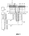
- FIG. 1 is a preferred device suitable for carrying out the claimed method shown schematically.
- the figure shows a vertical section through the device in side view.
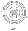
- Figure 2 is a horizontal section through the polishing plate of the device shown in top view.
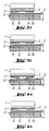
- FIGS. 3a, 3b and 4a, 4b show schematically like the geometry of semiconductor wafers through the application of the invention can be influenced.
- FIG. 1 In the embodiment shown is a single-side polishing machine with several polishing pots, one of which one can be seen.
- the polishing pot 1 presses a carrier plate 2 against with a polishing force K.
- the carrier plate is, for example held on the polishing pot by vacuum suction.
- the semiconductor wafers 5 are fixed on the front of the carrier plate 2 facing the polishing cloth 3. While of the polishing rotates both the carrier plate and the polishing plate with a certain Speed and direction of rotation.
- Essential feature of the device are ring combs running in concentric tracks in the polishing plate which flows a tempering medium.
- the temperature control medium is through flow lines VZ1 to VZ5 pumped into the respective ring chambers and leaves them again through return lines RZ1 to RZ5.
- the supply and return lines run through a rotating union 6, which is attached to the underside of the polishing plate 4. For the sake of clarity, the supply and return lines are shown interrupted.
- the temperature control medium is from a thermostat 7 at a desired temperature held.
- the thermostat is operated by one Control computer 8 controlled, the target temperatures SZ1 to SZ5 specifies for the temperature control medium in the annular chambers Z1 to Z5.
- the master computer accesses a data store 9 back, stored in the measurement data of previous polishing runs and automatically calculates the Target temperatures.
- the temperature control medium holds a certain one in each annular chamber Temperature upright, so that on the polishing plate radially symmetrical Areas with a characteristic temperature arise that sweep over the semiconductor wafers during polishing.
- the number of available areas depends on the number of the provided ring chambers.
- the radial widths of the areas are of the chosen radial widths of the annular chambers and depending on the temperature of the temperature control medium flows through the annular chambers.
- FIG 2 is a horizontal section through the polishing plate the device shown in Figure 1 in plan view. If the temperature of the temperature control medium in each ring chamber Z1 to Z5 from the temperatures of the tempering medium in the rest Differentiates annular chambers, produce the annular chambers the polishing plate corresponds to the number of annular chambers Number of annular areas. These areas are on a Temperature maintained, which is essentially the temperature of the Temperature control medium in the associated ring chamber corresponds. The Number of areas is correspondingly lower when the temperature of the temperature control medium in two or more neighboring ones Annular chambers is the same.
- Is the temperature of the temperature control medium the same in two adjacent ring chambers results from this an area on the polishing plate whose radial width is approximately the sum of the redial widths of these annular chambers equivalent. 2 to 5 annular chambers are preferred provided.
- the radial widths of the annular chambers are preferably 25 to 120% of the diameter of the to be polished Semiconductor wafers.
- the annular chambers can deviate from the illustration in Fig. 2 also be structured in itself (for example meandering).
- the specification of a certain radial temperature profile the polishing plate by providing areas with a certain temperature can also be considered other than described above can be achieved, for example by the integration of heating and cooling elements in the polishing plate. These can be done inductively or through a likewise in the polishing plate housed power supply are operated.
- FIGS. 3a, 3b and 4a, 4b show schematically like the geometry of semiconductor wafers through the application the invention can be influenced.
- the figures reflect that Result of exemplary embodiments.
Landscapes
- Engineering & Computer Science (AREA)
- Mechanical Engineering (AREA)
- Finish Polishing, Edge Sharpening, And Grinding By Specific Grinding Devices (AREA)
- Mechanical Treatment Of Semiconductor (AREA)
Description
Claims (7)
- Verfahren zum Polieren von Halbleiterscheiben, bei dem mindestens eine Seite mindestens einer Halbleiterscheibe gegen einen mit einem Poliertuch bespannten Polierteller gedrückt und poliert wird, wobei die Halbleiterscheibe und der Polierteller eine Relativbewegung ausführen, dadurch gekennzeichnet, daß die Halbleiterscheibe während des Polierens mindestens zwei Bereiche auf dem Polierteller überstreicht, die bestimmte radiale Breiten aufweisen und unterschiedliche Temperaturen haben, und Temperiermittel im Polierteller vorgesehen sind, mit deren Hilfe die Anzahl, die radialen Breiten und die Temperaturen der Bereiche vor dem Polieren der Halbleiterscheiben festgelegt werden.
- Verfahren nach Anspruch 1, dadurch gekennzeichnet, daß die Bereiche in Draufsicht auf den Polierteller konzentrische Ringe ausbilden.
- Verfahren nach Anspruch 1 oder Anspruch 2, dadurch gekennzeichnet, daß die Anzahl, die radialen Breiten und die Temperaturen der Bereiche in Abhängigkeit des Ergebnisses einer während einer vorangegangenen Polierfahrt durchgeführten Messung des radialen Temperaturprofils des Poliertellers festgelegt werden.
- Verfahren nach Anspruch 1 oder Anspruch 2, dadurch gekennzeichnet, daß die Anzahl, die radialen Breiten und die Temperaturen der Bereiche in Abhängigkeit des Ergebnisses einer Analyse der Geometrie von zuvor polierten Halbleiterscheiben festgelegt werden.
- Verfahren nach einem der Ansprüche 1 bis 4, dadurch gekennzeichnet, daß die Anzahl, die radialen Breiten und die Temperaturen der Bereiche rechnergestützt und automatisch festgelegt werden.
- Verfahren nach einem der Ansprüche 1 bis 5, dadurch gekennzeichnet, daß die Temperaturen der Bereiche während des Polierens verändert werden.
- Verfahren nach einem der Ansprüche 1 bis 6, dadurch gekennzeichnet, das das Polieren ausgewählt ist aus einer Gruppe von Polierverfahren, die die Einseitenpolitur, die Doppelseitenpolitur, die Einscheibenpolitur und die Mehrscheibenpolitur umfaßt.
Applications Claiming Priority (2)
| Application Number | Priority Date | Filing Date | Title |
|---|---|---|---|
| DE19748020 | 1997-10-30 | ||
| DE19748020A DE19748020A1 (de) | 1997-10-30 | 1997-10-30 | Verfahren und Vorrichtung zum Polieren von Halbleiterscheiben |
Publications (2)
| Publication Number | Publication Date |
|---|---|
| EP0916450A1 EP0916450A1 (de) | 1999-05-19 |
| EP0916450B1 true EP0916450B1 (de) | 2002-01-09 |
Family
ID=7847146
Family Applications (1)
| Application Number | Title | Priority Date | Filing Date |
|---|---|---|---|
| EP98119004A Expired - Lifetime EP0916450B1 (de) | 1997-10-30 | 1998-10-08 | Verfahren und Vorrichtung zum Polieren von Halbleiterscheiben |
Country Status (8)
| Country | Link |
|---|---|
| US (1) | US6095898A (de) |
| EP (1) | EP0916450B1 (de) |
| JP (1) | JPH11207605A (de) |
| KR (1) | KR100315162B1 (de) |
| DE (2) | DE19748020A1 (de) |
| MY (1) | MY133888A (de) |
| SG (1) | SG75876A1 (de) |
| TW (1) | TW407311B (de) |
Families Citing this family (32)
| Publication number | Priority date | Publication date | Assignee | Title |
|---|---|---|---|---|
| US5700180A (en) | 1993-08-25 | 1997-12-23 | Micron Technology, Inc. | System for real-time control of semiconductor wafer polishing |
| JP3693483B2 (ja) * | 1998-01-30 | 2005-09-07 | 株式会社荏原製作所 | 研磨装置 |
| US6020262A (en) * | 1998-03-06 | 2000-02-01 | Siemens Aktiengesellschaft | Methods and apparatus for chemical mechanical planarization (CMP) of a semiconductor wafer |
| US6352466B1 (en) * | 1998-08-31 | 2002-03-05 | Micron Technology, Inc. | Method and apparatus for wireless transfer of chemical-mechanical planarization measurements |
| JP2000334658A (ja) * | 1999-05-28 | 2000-12-05 | Fujitsu Ltd | ラップ加工装置 |
| US6358119B1 (en) * | 1999-06-21 | 2002-03-19 | Taiwan Semiconductor Manufacturing Company | Way to remove CU line damage after CU CMP |
| US6244944B1 (en) * | 1999-08-31 | 2001-06-12 | Micron Technology, Inc. | Method and apparatus for supporting and cleaning a polishing pad for chemical-mechanical planarization of microelectronic substrates |
| DE10009656B4 (de) * | 2000-02-24 | 2005-12-08 | Siltronic Ag | Verfahren zur Herstellung einer Halbleiterscheibe |
| DE10012840C2 (de) * | 2000-03-16 | 2001-08-02 | Wacker Siltronic Halbleitermat | Verfahren zur Herstellung einer Vielzahl von polierten Halbleiterscheiben |
| KR100413493B1 (ko) * | 2001-10-17 | 2004-01-03 | 주식회사 하이닉스반도체 | 화학적 기계적 연마 장치의 연마 플래튼 및 그를 이용한평탄화방법 |
| JP4510362B2 (ja) * | 2001-11-30 | 2010-07-21 | 俊郎 土肥 | Cmp装置およびcmp方法 |
| US20050161814A1 (en) * | 2002-12-27 | 2005-07-28 | Fujitsu Limited | Method for forming bumps, semiconductor device and method for manufacturing same, substrate processing apparatus, and semiconductor manufacturing apparatus |
| DE102004017452A1 (de) * | 2004-04-08 | 2005-11-03 | Siltronic Ag | Vorrichtung zur flächigen, abrasiven Bearbeitung eines scheibenförmigen Werkstücks |
| US20060226123A1 (en) * | 2005-04-07 | 2006-10-12 | Applied Materials, Inc. | Profile control using selective heating |
| US7201634B1 (en) | 2005-11-14 | 2007-04-10 | Infineon Technologies Ag | Polishing methods and apparatus |
| US20070227901A1 (en) * | 2006-03-30 | 2007-10-04 | Applied Materials, Inc. | Temperature control for ECMP process |
| DE102006032455A1 (de) * | 2006-07-13 | 2008-04-10 | Siltronic Ag | Verfahren zum gleichzeitigen beidseitigen Schleifen mehrerer Halbleiterscheiben sowie Halbleierscheibe mit hervorragender Ebenheit |
| DE102007063232B4 (de) * | 2007-12-31 | 2023-06-22 | Advanced Micro Devices, Inc. | Verfahren zum Polieren eines Substrats |
| US8149256B2 (en) * | 2008-06-04 | 2012-04-03 | Varian Semiconductor Equipment Associates, Inc. | Techniques for changing temperature of a platen |
| US20100279435A1 (en) * | 2009-04-30 | 2010-11-04 | Applied Materials, Inc. | Temperature control of chemical mechanical polishing |
| TWI825043B (zh) | 2017-11-14 | 2023-12-11 | 美商應用材料股份有限公司 | 用於化學機械研磨的溫度控制的方法與系統 |
| US11597052B2 (en) | 2018-06-27 | 2023-03-07 | Applied Materials, Inc. | Temperature control of chemical mechanical polishing |
| TWI885783B (zh) | 2019-02-20 | 2025-06-01 | 美商應用材料股份有限公司 | 化學機械拋光裝置及化學機械拋光方法 |
| TWI859239B (zh) | 2019-05-29 | 2024-10-21 | 美商應用材料股份有限公司 | 用於化學機械研磨系統的蒸氣處置站的設備及方法 |
| US11628478B2 (en) | 2019-05-29 | 2023-04-18 | Applied Materials, Inc. | Steam cleaning of CMP components |
| US11633833B2 (en) | 2019-05-29 | 2023-04-25 | Applied Materials, Inc. | Use of steam for pre-heating of CMP components |
| US11897079B2 (en) | 2019-08-13 | 2024-02-13 | Applied Materials, Inc. | Low-temperature metal CMP for minimizing dishing and corrosion, and improving pad asperity |
| TWI912098B (zh) | 2019-08-13 | 2026-01-11 | 美商應用材料股份有限公司 | 化學機械研磨系統 |
| WO2022006008A1 (en) | 2020-06-29 | 2022-01-06 | Applied Materials, Inc. | Control of steam generation for chemical mechanical polishing |
| CN115103738A (zh) | 2020-06-29 | 2022-09-23 | 应用材料公司 | Cmp中的温度和浆体流动速率控制 |
| US11577358B2 (en) | 2020-06-30 | 2023-02-14 | Applied Materials, Inc. | Gas entrainment during jetting of fluid for temperature control in chemical mechanical polishing |
| CN115461193A (zh) | 2020-06-30 | 2022-12-09 | 应用材料公司 | 用于cmp温度控制的设备和方法 |
Family Cites Families (6)
| Publication number | Priority date | Publication date | Assignee | Title |
|---|---|---|---|---|
| DE2809274A1 (de) * | 1978-03-03 | 1979-09-13 | Wacker Chemitronic | Verfahren zur vergleichmaessigung des polierabtrages von scheiben beim polieren |
| DE3128880C2 (de) * | 1981-07-22 | 1987-03-19 | Fa. Peter Wolters, 2370 Rendsburg | Maschine zum Läppen oder Polieren |
| JPH0659623B2 (ja) * | 1984-03-23 | 1994-08-10 | 株式会社日立製作所 | ウェハのメカノケミカルポリシング加工方法および装置 |
| US5036630A (en) * | 1990-04-13 | 1991-08-06 | International Business Machines Corporation | Radial uniformity control of semiconductor wafer polishing |
| JP2985490B2 (ja) * | 1992-02-28 | 1999-11-29 | 信越半導体株式会社 | 研磨機の除熱方法 |
| US5873769A (en) * | 1997-05-30 | 1999-02-23 | Industrial Technology Research Institute | Temperature compensated chemical mechanical polishing to achieve uniform removal rates |
-
1997
- 1997-10-30 DE DE19748020A patent/DE19748020A1/de not_active Withdrawn
-
1998
- 1998-09-15 SG SG1998003674A patent/SG75876A1/en unknown
- 1998-10-08 DE DE59802824T patent/DE59802824D1/de not_active Expired - Lifetime
- 1998-10-08 EP EP98119004A patent/EP0916450B1/de not_active Expired - Lifetime
- 1998-10-09 MY MYPI98004632A patent/MY133888A/en unknown
- 1998-10-22 KR KR1019980044284A patent/KR100315162B1/ko not_active Expired - Lifetime
- 1998-10-28 JP JP30728298A patent/JPH11207605A/ja active Pending
- 1998-10-28 TW TW087117834A patent/TW407311B/zh not_active IP Right Cessation
- 1998-10-28 US US09/181,428 patent/US6095898A/en not_active Expired - Lifetime
Also Published As
| Publication number | Publication date |
|---|---|
| KR19990037292A (ko) | 1999-05-25 |
| DE59802824D1 (de) | 2002-02-28 |
| JPH11207605A (ja) | 1999-08-03 |
| DE19748020A1 (de) | 1999-05-06 |
| MY133888A (en) | 2007-11-30 |
| KR100315162B1 (ko) | 2002-06-20 |
| TW407311B (en) | 2000-10-01 |
| US6095898A (en) | 2000-08-01 |
| SG75876A1 (en) | 2000-10-24 |
| EP0916450A1 (de) | 1999-05-19 |
Similar Documents
| Publication | Publication Date | Title |
|---|---|---|
| EP0916450B1 (de) | Verfahren und Vorrichtung zum Polieren von Halbleiterscheiben | |
| DE69611851T2 (de) | Haltevorrichtung für ein Substrat und Verfahren und Vorrichtung zum Polieren eines Substrates | |
| DE2462565C2 (de) | Preßeinrichtung mit Preßstempel zum Befestigen von mehreren Halbleiterwerkstücken auf einer Montageplatte | |
| EP0004033B1 (de) | Verfahren zur Vergleichmässigung des Polierabtrages von Scheiben beim Polieren | |
| DE102005045081B4 (de) | Suszeptor | |
| DE3112019C2 (de) | ||
| EP0847835B1 (de) | Verfahren und Vorrichtung zum Polieren von Halbleiterscheiben | |
| DE112016005417B4 (de) | Waferpolierverfahren | |
| DE69302944T2 (de) | Poliervorrichtung und Verfahren zur Ableitung deren Wärme | |
| DE102007056628B4 (de) | Verfahren und Vorrichtung zum gleichzeitigen Schleifen mehrerer Halbleiterscheiben | |
| DE2132174A1 (de) | Verfahren und Vorrichtung zum Herstellen eines dielektrisch isolierten Halbleitergebildes | |
| DE112016005920B4 (de) | Verfahren zum beidseitigen Polieren eines Wafers, Verfahren zum Herstellen eines Epitaxialwafers und Verwendung desselben sowie Epitaxialwafer | |
| DE112005001447B4 (de) | Doppelseitenpolierträger und Herstellungsverfahren desselben | |
| DE4105145A1 (de) | Verfahren und vorrichtung zum planar-schleifen der oberflaeche eines dielektrikums, das auf einem halbleiter-substrat aufgebracht ist | |
| DE112015006224B4 (de) | Einzelwaferverarbeitungsverfahren zum polieren einer seite eines halbleiterwafers und einzelwaferverarbeitungsvorrichtung zum polieren einer seite eines halbleiterwafers | |
| DE102011082777A1 (de) | Verfahren zum beidseitigen Polieren einer Halbleiterscheibe | |
| DE19543847A1 (de) | Poliervorrichtung | |
| DE112013006059T5 (de) | Doppelseiten-Poliermaschine mit einer Trägerplattenparallelitätssteuerung | |
| DE102017210423A1 (de) | Verfahren, Steuerungssystem und Anlage zum Bearbeiten einer Halbleiterscheibe sowie Halbleiterscheibe | |
| DE102008056276B4 (de) | Verfahren zur Regelung des Arbeitsspalts einer Doppelseitenbearbeitungsmaschine | |
| DE102010026987A1 (de) | Herstellvorrichtung und -verfahren für Halbleiterbauelement | |
| DE69934652T2 (de) | Mehrteiliger Polierkissen-Aufbau fór chemisch-mechanisches Polierverfahren | |
| DE3033944A1 (de) | Laeppvorrichtung fuer duenne plaettchen und aufspannvorrichtung fuer dieselben als teil der laeppvorrichtung | |
| DE60110819T2 (de) | Vorrichtung zum polieren von scheibenartigen gegenständen | |
| DE10261306A1 (de) | Haltering mit reduzierter Abnutzungs- und Kontaminationsrate für einen Polierkopf einer CMP-Anlage |
Legal Events
| Date | Code | Title | Description |
|---|---|---|---|
| PUAI | Public reference made under article 153(3) epc to a published international application that has entered the european phase |
Free format text: ORIGINAL CODE: 0009012 |
|
| 17P | Request for examination filed |
Effective date: 19981008 |
|
| AK | Designated contracting states |
Kind code of ref document: A1 Designated state(s): DE FI GB IT |
|
| AX | Request for extension of the european patent |
Free format text: AL;LT;LV;MK;RO;SI |
|
| 17Q | First examination report despatched |
Effective date: 19990518 |
|
| AKX | Designation fees paid |
Free format text: DE FI GB IT |
|
| GRAG | Despatch of communication of intention to grant |
Free format text: ORIGINAL CODE: EPIDOS AGRA |
|
| GRAG | Despatch of communication of intention to grant |
Free format text: ORIGINAL CODE: EPIDOS AGRA |
|
| GRAH | Despatch of communication of intention to grant a patent |
Free format text: ORIGINAL CODE: EPIDOS IGRA |
|
| GRAH | Despatch of communication of intention to grant a patent |
Free format text: ORIGINAL CODE: EPIDOS IGRA |
|
| GRAA | (expected) grant |
Free format text: ORIGINAL CODE: 0009210 |
|
| REG | Reference to a national code |
Ref country code: GB Ref legal event code: IF02 |
|
| AK | Designated contracting states |
Kind code of ref document: B1 Designated state(s): DE FI GB IT |
|
| REF | Corresponds to: |
Ref document number: 59802824 Country of ref document: DE Date of ref document: 20020228 |
|
| GBT | Gb: translation of ep patent filed (gb section 77(6)(a)/1977) |
Effective date: 20020406 |
|
| PG25 | Lapsed in a contracting state [announced via postgrant information from national office to epo] |
Ref country code: GB Free format text: LAPSE BECAUSE OF NON-PAYMENT OF DUE FEES Effective date: 20021008 Ref country code: FI Free format text: LAPSE BECAUSE OF NON-PAYMENT OF DUE FEES Effective date: 20021008 |
|
| PLBE | No opposition filed within time limit |
Free format text: ORIGINAL CODE: 0009261 |
|
| STAA | Information on the status of an ep patent application or granted ep patent |
Free format text: STATUS: NO OPPOSITION FILED WITHIN TIME LIMIT |
|
| 26N | No opposition filed | ||
| GBPC | Gb: european patent ceased through non-payment of renewal fee |
Effective date: 20021008 |
|
| PG25 | Lapsed in a contracting state [announced via postgrant information from national office to epo] |
Ref country code: IT Free format text: LAPSE BECAUSE OF NON-PAYMENT OF DUE FEES;WARNING: LAPSES OF ITALIAN PATENTS WITH EFFECTIVE DATE BEFORE 2007 MAY HAVE OCCURRED AT ANY TIME BEFORE 2007. THE CORRECT EFFECTIVE DATE MAY BE DIFFERENT FROM THE ONE RECORDED. Effective date: 20051008 |
|
| PGFP | Annual fee paid to national office [announced via postgrant information from national office to epo] |
Ref country code: DE Payment date: 20171019 Year of fee payment: 20 |
|
| REG | Reference to a national code |
Ref country code: DE Ref legal event code: R071 Ref document number: 59802824 Country of ref document: DE |