EP0923111A2 - Halbleiter-Montageeinrichtung mit einem hin und her geführten Chipgreifer - Google Patents
Halbleiter-Montageeinrichtung mit einem hin und her geführten Chipgreifer Download PDFInfo
- Publication number
- EP0923111A2 EP0923111A2 EP98811128A EP98811128A EP0923111A2 EP 0923111 A2 EP0923111 A2 EP 0923111A2 EP 98811128 A EP98811128 A EP 98811128A EP 98811128 A EP98811128 A EP 98811128A EP 0923111 A2 EP0923111 A2 EP 0923111A2
- Authority
- EP
- European Patent Office
- Prior art keywords
- lever
- swivel
- pivot
- chip
- levers
- Prior art date
- Legal status (The legal status is an assumption and is not a legal conclusion. Google has not performed a legal analysis and makes no representation as to the accuracy of the status listed.)
- Granted
Links
Images


Classifications
-
- H—ELECTRICITY
- H10—SEMICONDUCTOR DEVICES; ELECTRIC SOLID-STATE DEVICES NOT OTHERWISE PROVIDED FOR
- H10P—GENERIC PROCESSES OR APPARATUS FOR THE MANUFACTURE OR TREATMENT OF DEVICES COVERED BY CLASS H10
- H10P72/00—Handling or holding of wafers, substrates or devices during manufacture or treatment thereof
- H10P72/04—Apparatus for manufacture or treatment
- H10P72/0446—Apparatus for mounting on conductive members, e.g. leadframes or conductors on insulating substrates
-
- Y—GENERAL TAGGING OF NEW TECHNOLOGICAL DEVELOPMENTS; GENERAL TAGGING OF CROSS-SECTIONAL TECHNOLOGIES SPANNING OVER SEVERAL SECTIONS OF THE IPC; TECHNICAL SUBJECTS COVERED BY FORMER USPC CROSS-REFERENCE ART COLLECTIONS [XRACs] AND DIGESTS
- Y10—TECHNICAL SUBJECTS COVERED BY FORMER USPC
- Y10T—TECHNICAL SUBJECTS COVERED BY FORMER US CLASSIFICATION
- Y10T29/00—Metal working
- Y10T29/53—Means to assemble or disassemble
- Y10T29/5313—Means to assemble electrical device
- Y10T29/53174—Means to fasten electrical component to wiring board, base, or substrate
- Y10T29/53178—Chip component
-
- Y—GENERAL TAGGING OF NEW TECHNOLOGICAL DEVELOPMENTS; GENERAL TAGGING OF CROSS-SECTIONAL TECHNOLOGIES SPANNING OVER SEVERAL SECTIONS OF THE IPC; TECHNICAL SUBJECTS COVERED BY FORMER USPC CROSS-REFERENCE ART COLLECTIONS [XRACs] AND DIGESTS
- Y10—TECHNICAL SUBJECTS COVERED BY FORMER USPC
- Y10T—TECHNICAL SUBJECTS COVERED BY FORMER US CLASSIFICATION
- Y10T29/00—Metal working
- Y10T29/53—Means to assemble or disassemble
- Y10T29/5313—Means to assemble electrical device
- Y10T29/53174—Means to fasten electrical component to wiring board, base, or substrate
- Y10T29/53183—Multilead component
Definitions
- the invention relates to a semiconductor assembly device a chip gripper, which is between a first location and a second location can be moved back and forth by means of a lever mechanism is a chip from a chip carrier at the first location lift off and place the chip on a substrate at the second location.
- a chip gripper which is between a first location and a second location can be moved back and forth by means of a lever mechanism is a chip from a chip carrier at the first location lift off and place the chip on a substrate at the second location.
- Such a device known as a "pick-and-place” is part of an assembly machine called “Die Bonder” used in semiconductor assembly. It serves the numerous, similar chips of a wafer that are next to each other on a carrier, one after the other on a Substrate, e.g. a metallic leadframe.
- Chip ready at said first location Chip ready at said first location, and so will the substrate moved to a new substrate location at the second location to provide.
- the chip gripper can be raised and lowered in a known manner, either together with the whole facility or on its own relative to the facility.
- the aim of the invention is for a semiconductor assembly device of the type mentioned above, when State of the art to overcome existing disadvantages.
- Movement mechanism is primarily intended to ensure accurate positioning ensure the chip gripper in the two end positions, doing so but also quick back and forth movements, i.e. short cycle times enable.
- the Lever mechanism of the device on a first pivot lever sits and with alternating swivel direction between two end positions in which it is driven to the side of one or the other place.
- a second swivel lever is mounted at the end of the first pivot lever. He is with respect to the pivot direction of the first pivot lever in opposite directions as well as with a specific translation for its pivoting movement driven; at its end he is with the chip gripper connected.
- the translation mentioned and the lengths of both Swivel levers are coordinated in a certain way, namely, that in the two end positions of the first pivot lever both swivel levers are in the extended position and the chip gripper has reached one or the other location is.
- the invention is above all It is essential that at the end of each movement game the Chip gripper its end position (i.e. the first or the second Location) each in the direction of the extended swivel lever reached, so any movement component disappears in the end positions transverse to the longitudinal direction of the lever. Also the The mass force of the accelerated chip gripper then acts in the direction the extended lever and helps to a certain extent for stabilization the stretch position at.
- a lever mechanism with these parameters is known per se as so-called Straight guidance, which means that a body moved by it - here the chip gripper - moves on a straight line.
- the device according to the invention is but basically also with other parameters (even with not integer values of n) can be realized.
- Special further configurations that defined in claim 1, according to the invention Means are specified in the dependent claims.
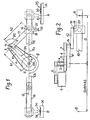
- the Bonders 1 and 2 is part of the semiconductor assembly device one not shown and known per se, Assembly machines called "The Bonders". It is used by means of of a chip gripper 20 in cycles at a first location A to lift a semiconductor chip 30 off a chip carrier 32 and, after moving the chip gripper, the chip in a second place B to be placed on a substrate 38 (“pick-and-place”).
- the chip carrier 32 typically an adhesive film
- the Chip carrier 32 with the chips one Wafers 35 are located on a sliding wafer table 34, which each provides a next chip 30 at location A.
- the Substrate 38 e.g. a metallic lead frame lies on top of one referred to as "indexer" shifter 36, the advances the substrate step by step to one at location B.
- the chip gripper 20 Part of a so-called bond head
- the pick-and-place facility can be raised and lowered, but it can also be Device as a whole vertically movable (seen in Fig. 1) be executed.
- the pick-and-place device according to FIGS. 1 and 2 has one first pivot lever 10 which is stuck on a shaft 4.
- the Shaft 4 is located in the middle between locations A and B (bearing 3, Fig. 2), i.e. the pivot axis of the lever 10 has the same Distance S to A and B on.
- a second pivot lever 12 is mounted by means of the shaft 14 at the end of the first pivot lever. The end of the second lever is in turn via an axis 16 connected to a carriage 18. This carries the chip gripper 20 and slides along a linear guide 19, which is between A and B extends.
- a fixed rotary actuator e.g. consisting of engine 1 and Toothed belt gear 2 (only indicated in Fig. 2) drives the first lever 10 via the shaft 4 with changing pivoting direction on.
- the lever 10 covers a swivel range ⁇ between two end positions Ea, Eb, in which it each has a location A or points to the other location B.
- Fig. 1 are the end positions the swivel lever and the chip gripper are indicated by dash-dotted lines, an intermediate position (with the swivel angle ⁇ 1 of the lever 10) drawn with solid lines.
- the end positions Ea and Eb of the first angle lever 10 are replaced by a suitable one Drive control of motor 1 determined and adhered to.
- the second pivot lever 12 is not “passive" by the first lever 10 taken, but experiences a drive with certain Translation relative to and opposite to the first lever Swivel direction. According to the example shown, this is Drive realized by means of a toothed belt 6, which has a fixed, to the shaft 4 coaxial gear 5 and one on the shaft 14 fixed gear 7 wraps around (instead of the toothed belt 6 could also be an intermediate gear mounted on the lever 12 provide, which meshes with the gears 5 and 7). With that the pivoting movements of the two levers 10 and 12 (pivot angle ⁇ 1 or ⁇ 2) coupled with each other in a certain way.
- the translation n between the levers 10 and 12 is 2 , ie in each lever position the angle ⁇ 2 of the lever 12 relative to the lever 10 is twice the pivoting angle ⁇ 1 of the lever 10. Furthermore, it is essential that the Levers 10 and 12 have the same lengths h1 and h2 and the sum of both lever lengths h1 + h2 is equal to the distance S.
- the lever mechanism according to FIGS. 1 and 2 has the properties straight guidance, i.e. the end of the second pivot lever 12 (Axis 16) moves on a straight line G. This means that from the carriage 18 no transverse forces or moments on the Linear guide 19 are exercised. This leadership and the articulated Connection between carriage 18 and lever 12 have in essential only the function, the orientation of the chip gripper to maintain during its displacement (with rigid connection between lever 12 and chip gripper 20 the latter would together with the transported chip 30 each by 180 ° - based on the levels of the chip carrier 32 and the substrate 38 - turned). As can easily be seen with reference to FIG.
- FIG. 3 shows the time course of the path s Velocity v and acceleration a at the end of the second Swivel lever (axis 16) during a movement game from A to B or vice versa, under the idealized assumption that the Swivel angle ⁇ 1 is linear with time t.
- 1 and 2 all run in the lever mechanism three sizes s, v and a according to harmonic functions. In the alternating movement is a sudden start and stopping the drive, as assumed in FIG. 3, does not realistic.
- 4 shows a corresponding one Course of s, v and a under practical conditions with "Gentle" start-up and braking of the drive in the area of the end positions.
- the pivoting movements take place the levers 10 and 12 in vertical planes, i.e. vertically to chip carrier 32 and to substrate 38
- the pivot axes of the levers stand vertically and the levers accordingly horizontally move in levels that correspond to the levels of the chip carrier and the Substrate parallel.
- the chip gripper can then with the End of the second pivot lever to be rigidly connected, and one Longitudinal guide (corresponding to the linear guide 19 in Fig. 1 and 2) is then generally not necessary.
- one Longitudinal guide corresponding to the linear guide 19 in Fig. 1 and 2
- End stops can also be used in such an embodiment variant for the vertical and lateral position of the chip gripper (or the second swivel lever) be appropriate.
- FIG. 5 shows a further example of a device according to the invention
- Semiconductor assembly device shown in floor plan, with horizontally pivoted pivoting levers 10 ', 12' and compared to the example of FIGS. 1 and 2 changed parameters.
- the axis 4 'of the first pivot lever 10' is on the perpendicular M stored between A and B so that in the end positions Ea and Eb the lever 10 'and the one in the extended position relative to it point second pivot lever 12 'to location A or B.
- the here chip gripper rigidly connected to the end of the second lever 12 ' 20 'then stands above location A or B.
- the alternating one (Not shown) pivot drive of the lever 10 ' can be analog 2, but the Swivel range, as mentioned, is only 120 °.
- the end positions Ea and Eb are in turn by appropriate control of the drive motor certainly.
- opposite drive of the second pivot lever 12 'again serves a toothed belt 6', which the fixed gear 5 'and the gear 7' loops.
- the latter is connected to the lever 12 'via the shaft 14', and its number of teeth is 1/3 of that of the wheel 5 '. Therefore is the pivot angle ⁇ 2 of the lever 12 'relative to the lever 10 'always three times the swivel angle ⁇ 1 of the lever 10'.
- Each chip 30 undergoes a rotation of on the way from A to B. 120 °.
- the wafer 35 must therefore correspond to the chip edges be oriented parallel and perpendicular to Ea, and also the displacements of the wafer table 34 must of course be so directed be as indicated by arrows in FIG. 5.
- the formation of the Pick and Place facility with the two Swivel levers 10 'and 12' also allow the use of Stop or limiting means that the movement of the Lead chip gripper 20 in the end positions Ea and Eb and thus Swing the pivot lever 10 'and 12' and thus the Effectively prevent chip gripper 20 during a rapid stop.
- the Fig. 6 shows the pivot lever 12 'just before it reaches the end position Eb reached.
- the pivot lever 12 ' has a T-shaped end 41 two end faces 41a and 41b.
- the center of the chip gripper 20 moves along the dashed line 42.
- the ends 41a and 41b move along curves 43a and 43b, respectively.
- Stop means are used instead of the linear guide 19.
Landscapes
- Die Bonding (AREA)
- Transmission Devices (AREA)
- Manipulator (AREA)
- Container, Conveyance, Adherence, Positioning, Of Wafer (AREA)
- Manufacture Of Motors, Generators (AREA)
- Specific Conveyance Elements (AREA)
- Feeding Of Workpieces (AREA)
- Sheets, Magazines, And Separation Thereof (AREA)
Abstract
Description
- Fig. 1
- ist die Seitenansicht eines ersten Ausführungsbeispiels der erfindungsgemässen Halbleiter-Montageeinrichtung in vereinfachter Darstellung,
- Fig. 2
- ist die Draufsicht der Einrichtung nach Fig. 1 (Wafer und Substrat weggelassen),
- Fig. 3 und 4
- sind Zeitdiagramme zu der Einrichtung nach Fig. 1 und 2,
- Fig. 5
- veranschaulicht ein weiteres Ausführungsbeispiel in Draufsicht, und
- Fig. 6
- zeigt Anschlagsmittel.
Claims (9)
- Halbleiter-Montageeinrichtung mit einem Chipgreifer (20), welcher zwischen einem ersten Ort (A) und einem zweiten Ort (B) mittels eines Hebelmechanismus hin und her bewegbar ist, um jeweils am ersten Ort einen Chip (30) von einem Chipträger (32) abzuheben und am zweiten Ort den Chip auf ein Substrat (38) abzulegen, gekennzeichnetdurch einen ersten Schwenkhebel (10), der auf einer im gleichen Abstand (S) vom ersten (A) und vom zweiten Ort (B) gelagerten Antriebswelle (4) sitzt und mit wechselnder Schwenkrichtung zwischen zwei Endlagen (Ea, Eb) angetrieben ist, in denen der Schwenkhebel (10) je zur Seite des einen (A) oder des anderen Ortes (B) hin weist;und durch einen zweiten Schwenkhebel (12), der am Ende des ersten Schwenkhebels (10) gelagert und in Bezug auf dessen Schwenkrichtung gegensinnig und mit bestimmter Übersetzung (n) zu dessen Schwenkbewegung angetrieben ist und der an seinem Ende mit dem Chipgreifer (20) verbunden ist;wobei die genannte Übersetzung (n) und die Längen (h1, h2) beider Schwenkhebel (10, 12) so aufeinander abgestimmt sind, dass in beiden Endlagen (Ea, Eb) des ersten Schwenkhebels (10) beide Schwenkhebel (10, 12) sich zueinander in Strecklage befinden und der Chipgreifer (20) über dem einen (A) bzw. dem andern Ort (B) angelangt ist.
- Halbleiter-Montageeinrichtung nach Anspruch 1, dadurch gekennzeichnet, dass der Schwenkbereich (Φ) zwischen den Endlagen (Ea, Eb) des ersten Schwenkhebels (10) gleich 180°, die Übersetzung (n) zwischen beiden Schwenkhebeln (10, 12) gleich 2 und das Längenverhältnis (h1/h2) beider Schwenkhebel (10, 12) gleich 1 ist.
- Halbleiter-Montageeinrichtung nach Anspruch 1 oder 2, dadurch gekennzeichnet, dass am Ende des zweiten Schwenkhebels (12) ein Schlitten (18) angelenkt ist, der entlang eines Führungsorgans (19) verschiebbar ist und den Chipgreifer (20) trägt.
- Halbleiter-Montageeinrichtung nach einem der Ansprüche 1 bis 3, dadurch gekennzeichnet, dass die beiden Schwenkhebel (10, 12) in Ebenen schwenken, die senkrecht zum Substrat (38) stehen.
- Halbleiter-Montageeinrichtung nach 1, dadurch gekennzeichnet, dass die beiden Schwenkhebel (10', 12') in Ebenen schwenken, die parallel zum Substrat (38) liegen.
- Halbleiter-Montageeinrichtung nach Anspruch 5, dadurch gekennzeichnet, dass der Schwenkbereich (Φ) zwischen den Endlagen (Ea, Eb) des ersten Schwenkhebels (10') gleich 120°, die Übersetzung (n) zwischen beiden Schwenkhebeln (10, 12) gleich 3 und das Längenverhältnis (h1/h2) beider Schwenkhebel (10', 12') gleich 2 ist.
- Halbleiter-Montageeinrichtung nach Anspruch 5 oder 6, dadurch gekennzeichnet, dass der Chipgreifer (20') mit dem Ende des zweiten Schwenkhebels (12') starr verbunden ist.
- Halbleiter-Montageeinrichtung nach einem der Ansprüche 1 bis 7, dadurch gekennzeichnet, dass der zweite Schwenkhebel (12) auf einer Welle (14) gelagert ist, auf der ein Zahnrad (7) sitzt, welches von einem zur Antriebswelle (4) koaxialen, feststehenden Zahnrad (5) über einen Zahnriemen (6) oder ein am ersten Schwenkhebel (10) gelagertes Zwischenrad angetrieben ist.
- Halbleiter-Montageeinrichtung nach einem der Ansprüche 1 bis 8, dadurch gekennzeichnet, dass in den Endlagen (Ea, Eb) quer zur Bewegungsrichtung des Chipgreifers (20) angeordnete Anschlagsmittel (44) für den zweiten Schwenkhebel (12; 12') vorhanden sind.
Priority Applications (1)
| Application Number | Priority Date | Filing Date | Title |
|---|---|---|---|
| EP98811128A EP0923111B1 (de) | 1997-12-07 | 1998-11-11 | Halbleiter-Montageeinrichtung mit einem hin und her geführten Chipgreifer |
Applications Claiming Priority (5)
| Application Number | Priority Date | Filing Date | Title |
|---|---|---|---|
| CH280797 | 1997-12-07 | ||
| CH280797 | 1997-12-07 | ||
| EP98810426 | 1998-05-11 | ||
| EP98810426 | 1998-05-11 | ||
| EP98811128A EP0923111B1 (de) | 1997-12-07 | 1998-11-11 | Halbleiter-Montageeinrichtung mit einem hin und her geführten Chipgreifer |
Publications (3)
| Publication Number | Publication Date |
|---|---|
| EP0923111A2 true EP0923111A2 (de) | 1999-06-16 |
| EP0923111A3 EP0923111A3 (de) | 2004-12-29 |
| EP0923111B1 EP0923111B1 (de) | 2007-05-02 |
Family
ID=4242039
Family Applications (1)
| Application Number | Title | Priority Date | Filing Date |
|---|---|---|---|
| EP98811128A Expired - Lifetime EP0923111B1 (de) | 1997-12-07 | 1998-11-11 | Halbleiter-Montageeinrichtung mit einem hin und her geführten Chipgreifer |
Country Status (10)
| Country | Link |
|---|---|
| US (2) | US6185815B1 (de) |
| EP (1) | EP0923111B1 (de) |
| JP (1) | JP4220042B2 (de) |
| KR (1) | KR100550049B1 (de) |
| CN (1) | CN1130763C (de) |
| AT (1) | ATE361549T1 (de) |
| DE (1) | DE59813989D1 (de) |
| MY (1) | MY131974A (de) |
| SG (1) | SG74676A1 (de) |
| TW (1) | TW410413B (de) |
Cited By (11)
| Publication number | Priority date | Publication date | Assignee | Title |
|---|---|---|---|---|
| SG85730A1 (en) * | 1999-09-10 | 2002-01-15 | Esec Trading Sa | Method and apparatus for mounting semiconductor chips |
| EP1189496A1 (de) | 2000-09-13 | 2002-03-20 | Esec Trading S.A. | Vorrichtung für die Montage von Halbleiterchips |
| DE102004026534B4 (de) * | 2003-06-06 | 2007-09-27 | Esec Trading S.A. | Halbleiter-Montageeinrichtung |
| US7284318B2 (en) | 2001-12-05 | 2007-10-23 | Esec, Trading Sa | Apparatus for mounting semiconductor chips |
| DE102005029136B4 (de) * | 2004-07-02 | 2008-03-27 | Unaxis International Trading Ltd. | Verfahren und Einrichtung für die Montage von Halbleiterchips |
| CH697294B1 (de) * | 2003-12-22 | 2008-08-15 | Oerlikon Assembly Equipment Ag | Verfahren für die Kalibration der Greifachse des Bondkopfs eines Automaten für die Montage von Halbleiterchips auf einem Substrat. |
| DE102004043084B4 (de) * | 2003-09-12 | 2009-01-29 | Oerlikon Assembly Equipment Ag, Steinhausen | Einrichtung und Verfahren für die Montage oder Verdrahtung von Halbleiterchips |
| DE102007058802B3 (de) * | 2007-12-06 | 2009-06-10 | Datacon Technology Gmbh | Thermodenvorrichtung |
| WO2009037108A3 (de) * | 2007-09-18 | 2009-06-25 | Oerlikon Assembly Equipment Ag | Pick und place system für eine halbleiter-montageeinrichtung |
| DE112008002467T5 (de) | 2007-10-09 | 2010-08-26 | Esec Ag | Verfahren für die Entnahme von Halbleiterchips von einem Wafertisch und Verfahren für die Montage von Halbleiterchips auf einem Substrat |
| CN105460681A (zh) * | 2015-12-29 | 2016-04-06 | 重庆市大通茂纺织科技有限公司 | 单维度柔性物料铺平装置 |
Families Citing this family (22)
| Publication number | Priority date | Publication date | Assignee | Title |
|---|---|---|---|---|
| US6785815B1 (en) * | 1999-06-08 | 2004-08-31 | Intertrust Technologies Corp. | Methods and systems for encoding and protecting data using digital signature and watermarking techniques |
| DE19958328A1 (de) * | 1999-10-08 | 2001-07-12 | Flexchip Ag | Verfahren zum Herstellen einer elektrischen Verbindung zwischen Chip-Kontaktelemente-Einheiten und externen Kontaktanschlüssen |
| SG100644A1 (en) | 2000-04-04 | 2003-12-26 | Esec Trading Sa | Linear guide with air bearing |
| EP1253817A3 (de) * | 2001-04-23 | 2003-07-09 | Liconic Ag | Einrichtung zum Aufnehmen und Plazieren von kleinen Gegenständen |
| DE20116653U1 (de) * | 2001-05-07 | 2002-01-03 | Esec Trading S.A., Cham | Montageautomat für die Plazierung eines Halbleiterchips als Flipchip auf einem Substrat |
| US20040105750A1 (en) * | 2002-11-29 | 2004-06-03 | Esec Trading Sa, A Swiss Corporation | Method for picking semiconductor chips from a foil |
| US20050161814A1 (en) | 2002-12-27 | 2005-07-28 | Fujitsu Limited | Method for forming bumps, semiconductor device and method for manufacturing same, substrate processing apparatus, and semiconductor manufacturing apparatus |
| TWI231561B (en) * | 2003-05-21 | 2005-04-21 | Esec Trading Sa | Apparatus for mounting semiconductors |
| US7428958B2 (en) * | 2004-11-15 | 2008-09-30 | Nikon Corporation | Substrate conveyor apparatus, substrate conveyance method and exposure apparatus |
| TWI447840B (zh) * | 2004-11-15 | 2014-08-01 | 尼康股份有限公司 | 基板搬運裝置、基板搬運方法以及曝光裝置 |
| JP2006272523A (ja) * | 2005-03-30 | 2006-10-12 | Shinmei Ind Co Ltd | ワーク搬送装置 |
| US7569932B2 (en) * | 2005-11-18 | 2009-08-04 | Checkpoint Systems, Inc. | Rotary chip attach |
| WO2009047214A2 (en) * | 2007-10-09 | 2009-04-16 | Oerlikon Assembly Equipment Ag, Steinhausen | Method for picking up semiconductor chips from a wafer table and mounting the removed semiconductor chips on a substrate |
| JP4941422B2 (ja) * | 2008-07-14 | 2012-05-30 | パナソニック株式会社 | 部品実装システム |
| KR101493046B1 (ko) * | 2008-11-13 | 2015-02-12 | 삼성전자주식회사 | 유동 그리퍼를 포함하는 클램핑 장치 |
| CN102848377B (zh) * | 2011-06-28 | 2015-01-21 | 昆山市佰奥自动化设备科技有限公司 | 旋转摆动机械手臂 |
| KR101360634B1 (ko) * | 2013-03-08 | 2014-02-07 | 문정만 | 동력 전달 시스템 |
| CN103594382B (zh) * | 2013-11-21 | 2016-01-20 | 刘锦刚 | 一种由滑块驱动的竖直部分具有弹性材料的芯片安装装置 |
| FR3039743B1 (fr) | 2015-07-29 | 2017-07-21 | Jfp Microtechnic | Dispositif de manipulation de petits objets |
| JP6768454B2 (ja) * | 2016-11-08 | 2020-10-14 | コマツ産機株式会社 | ワーク搬送装置 |
| JP6618957B2 (ja) * | 2017-06-14 | 2019-12-11 | アイダエンジニアリング株式会社 | プレス機械のワーク搬送装置 |
| CN110597302A (zh) * | 2019-10-25 | 2019-12-20 | 浙江正泰新能源开发有限公司 | 光伏跟踪器系统 |
Family Cites Families (86)
| Publication number | Priority date | Publication date | Assignee | Title |
|---|---|---|---|---|
| US3337941A (en) | 1965-05-27 | 1967-08-29 | Ibm | Recycle control circuit for a chip positioning machine |
| US4144449A (en) | 1977-07-08 | 1979-03-13 | Sperry Rand Corporation | Position detection apparatus |
| US4151945A (en) | 1977-12-08 | 1979-05-01 | Universal Instruments Corporation | Automated hybrid circuit board assembly apparatus |
| DE2823360C3 (de) * | 1978-05-29 | 1981-06-25 | Texas Instruments Deutschland Gmbh, 8050 Freising | Vorrichtung zur Überführung von Gegenständen |
| US4351264A (en) | 1979-03-20 | 1982-09-28 | S&S Corrugated Paper Machinery Co., Inc. | Adhesive metering device |
| EP0020879A1 (de) | 1979-06-06 | 1981-01-07 | Erwin Sick GmbH Optik-Elektronik | Opto-elektronischer Abstandsmesser |
| JPS5645337A (en) | 1979-09-11 | 1981-04-25 | Hitachi Ltd | Feeding and assembling device for parts |
| DE2939102A1 (de) | 1979-09-27 | 1981-04-16 | Henkel KGaA, 4000 Düsseldorf | Klebstoffauftragsvorrichtung und verfahren zum betrieb derselben |
| US4461610A (en) * | 1980-06-02 | 1984-07-24 | Tdk Corporation | Apparatus for mounting chip type circuit elements on printed circuit boards |
| US4378134A (en) | 1981-10-19 | 1983-03-29 | Excellon Industries | Air bearing guide system |
| GB2111863B (en) | 1981-12-24 | 1985-09-04 | Thorn Consumer Electronics Lim | Spray apparatus and method of spraying articles and an article made by the method |
| US4606117A (en) * | 1983-05-13 | 1986-08-19 | Tdk Corporation | Apparatus for automatically mounting chip type circuit elements on printed circuit boards |
| JPS6012799A (ja) * | 1983-07-01 | 1985-01-23 | 三洋電機株式会社 | チップ状電子部品の自動装着装置 |
| FR2548857B1 (fr) | 1983-07-04 | 1987-11-27 | Cortaillod Cables Sa | Procede de fabrication en continu d'une carte imprimee |
| FR2548852A1 (fr) | 1983-07-08 | 1985-01-11 | Drubay Fernand | Reseau de communication de signaux video sous forme analogique |
| EP0144717B1 (de) | 1983-11-05 | 1988-10-19 | Zevatech AG | Verfahren und Vorrichtung zur Positionierung von Bauteilen auf einem Werkstück |
| US4584047A (en) | 1984-04-03 | 1986-04-22 | Monarch Marking Systems, Inc. | Hand-held labeler having improved web position sensing and print head control |
| US4586670A (en) | 1984-12-17 | 1986-05-06 | Usm Corporation | Tape stripper for electrical component tape feeder |
| US4610083A (en) | 1985-08-26 | 1986-09-09 | Zenith Electronics Corporation | Method and apparatus for electronic component matching |
| GB2183820A (en) | 1985-11-09 | 1987-06-10 | Dynapert Precima Ltd | Electronic component placement |
| JPS62144255U (de) | 1986-02-28 | 1987-09-11 | ||
| US4728252A (en) * | 1986-08-22 | 1988-03-01 | Lam Research Corporation | Wafer transport mechanism |
| JP2662948B2 (ja) | 1986-10-30 | 1997-10-15 | ニツト− システム テクノロジ− インコ−ポレ−テツド | チップテープのトップテープ除去装置 |
| DE3704505A1 (de) * | 1987-02-13 | 1988-08-25 | Leybold Ag | Einlegegeraet fuer vakuumanlagen |
| JPS63277166A (ja) * | 1987-05-09 | 1988-11-15 | Hitachi Ltd | チツプ電子部品供給装置 |
| US4937511A (en) * | 1987-07-21 | 1990-06-26 | Western Technologies Automation, Inc. | Robotic surface mount assembly system |
| KR970004947B1 (ko) * | 1987-09-10 | 1997-04-10 | 도오교오 에레구토론 가부시끼가이샤 | 핸들링장치 |
| US4924304A (en) | 1987-11-02 | 1990-05-08 | Mpm Corporation | Video probe aligning of object to be acted upon |
| CH674886A5 (de) | 1987-11-09 | 1990-07-31 | Alphasem Ag | |
| US4810154A (en) * | 1988-02-23 | 1989-03-07 | Molex Incorporated | Component feeder apparatus and method for vision-controlled robotic placement system |
| US4961893A (en) | 1988-04-28 | 1990-10-09 | Schlumberger Industries | Method for manufacturing memory cards |
| US4819326A (en) * | 1988-06-16 | 1989-04-11 | Stannek Karl H | Method for robotic placement of electronic parts on a circuit board |
| US4943342A (en) * | 1988-08-29 | 1990-07-24 | Golemon Valia S | Component feeding device for circuit board mounting apparatus |
| US5289625A (en) | 1989-04-05 | 1994-03-01 | Canon Kabushiki Kaisha | Method for supplying articles and apparatus therefor |
| JPH02303751A (ja) | 1989-05-17 | 1990-12-17 | Hitachi Ltd | 部品位置決め方法 |
| JPH038655A (ja) | 1989-06-02 | 1991-01-16 | Sanyo Electric Co Ltd | 部品供給テープの部品残量報知方式 |
| US5342460A (en) | 1989-06-13 | 1994-08-30 | Matsushita Electric Industrial Co., Ltd. | Outer lead bonding apparatus |
| JP2803221B2 (ja) * | 1989-09-19 | 1998-09-24 | 松下電器産業株式会社 | Ic実装装置及びその方法 |
| JPH03133763A (ja) | 1989-10-11 | 1991-06-06 | Sony Corp | 部品連装置及びその部品切れ検知システム |
| US5157734A (en) | 1989-12-19 | 1992-10-20 | Industrial Technology Research Institute | Method and apparatus for picking and placing a surface mounted device with the aid of machine vision |
| US5191693A (en) | 1989-12-29 | 1993-03-09 | Canon Kabushiki Kaisha | Tape type work conveying method and conveying apparatus |
| CA2044649A1 (en) | 1990-06-19 | 1991-12-20 | Masanori Nishiguchi | Method and apparatus for packaging a semiconductor device |
| JPH0469777A (ja) | 1990-07-10 | 1992-03-04 | Dainippon Screen Mfg Co Ltd | プリント基板のパターン検査装置 |
| JP2870142B2 (ja) | 1990-07-17 | 1999-03-10 | 日本電気株式会社 | コプラナリティ測定方法及びその装置 |
| US5213653A (en) | 1990-09-05 | 1993-05-25 | Yamaha Hatsudoki Kabushiki Kaisha | Waste tape disposing means of tape feeder |
| US5235164A (en) | 1990-09-19 | 1993-08-10 | Matsushita Electric Industrial Co., Ltd. | Parts supply device, parts supply method, parts managing system, and parts managing apparatus |
| US5400497A (en) | 1990-10-29 | 1995-03-28 | Matsushita Electric Industrial Co., Ltd. | Electronic parts mounting apparatus having memory equipped parts supply device |
| US5278634A (en) | 1991-02-22 | 1994-01-11 | Cyberoptics Corporation | High precision component alignment sensor system |
| US5248362A (en) | 1991-05-24 | 1993-09-28 | Interfic Developments, Inc. | Method for applying glue to the flute tips of a single-faced corrugated paperboard sheet |
| DE4119401C2 (de) | 1991-06-10 | 1998-07-23 | Finetech Ges Fuer Elektronik T | Vorrichtung zum Bestücken eines Schaltungsträgers mit elektronischen Bauelementen |
| US5309223A (en) | 1991-06-25 | 1994-05-03 | Cyberoptics Corporation | Laser-based semiconductor lead measurement system |
| US5195234A (en) | 1991-08-19 | 1993-03-23 | Motorola, Inc. | Method and apparatus for visual alignment of parts |
| DE4127696A1 (de) | 1991-08-21 | 1993-02-25 | Adalbert Fritsch | Vorrichtung zum positionieren von smd-bauelementen, insbesondere smd-chips |
| JPH0718448B2 (ja) | 1991-09-19 | 1995-03-06 | テイエチケー株式会社 | リニアベアリング用スライダ及びその製造法 |
| JPH05121470A (ja) * | 1991-10-29 | 1993-05-18 | Toshiba Corp | ダイボンダ装置 |
| JPH05145283A (ja) | 1991-11-15 | 1993-06-11 | Sony Corp | 部品情報読取装置 |
| US5275657A (en) | 1991-11-25 | 1994-01-04 | E. I. Du Pont De Nemours And Company | Apparatus for applying adhesive to a honeycomb half-cell structure |
| JPH05169885A (ja) | 1991-12-26 | 1993-07-09 | Mitsubishi Electric Corp | 薄型icカード |
| JP3008655B2 (ja) | 1992-04-01 | 2000-02-14 | ソニー株式会社 | 固体撮像装置 |
| US5547537A (en) | 1992-05-20 | 1996-08-20 | Kulicke & Soffa, Investments, Inc. | Ceramic carrier transport for die attach equipment |
| JPH0666319A (ja) | 1992-06-19 | 1994-03-08 | Nippon Thompson Co Ltd | 転がり案内ユニット及びその製造方法 |
| JPH0689910A (ja) | 1992-09-07 | 1994-03-29 | Toshiba Corp | ダイボンディング装置 |
| US5415693A (en) | 1992-10-01 | 1995-05-16 | Hitachi Techno Engineering Co., Ltd. | Paste applicator |
| JPH06302992A (ja) | 1993-04-14 | 1994-10-28 | Toshiba Corp | 部品実装機のカートリッジ構造及び部品実装機の管理システム |
| US5459794A (en) | 1993-07-15 | 1995-10-17 | Ninomiya; Takanori | Method and apparatus for measuring the size of a circuit or wiring pattern formed on a hybrid integrated circuit chip and a wiring board respectively |
| DE69426053T2 (de) | 1993-10-08 | 2001-06-21 | Valtac, Alex Beaud | Speicheranordnung |
| EP0649719B1 (de) | 1993-10-26 | 1997-10-01 | Siemens Aktiengesellschaft | Verfahren zur Herstellung von Chipkarten mittels Spritzgiessen |
| KR0163366B1 (ko) * | 1993-11-26 | 1999-02-01 | 오쿠라 고이치 | 펠레트 본딩장치 |
| JPH07157259A (ja) | 1993-12-02 | 1995-06-20 | Hitachi Ltd | 乗客コンベア乗り込み時の転倒防止装置 |
| CA2113752C (en) | 1994-01-19 | 1999-03-02 | Stephen Michael Rooks | Inspection system for cross-sectional imaging |
| US5559727A (en) | 1994-02-24 | 1996-09-24 | Quad Systems Corporation | Apparatus and method for determining the position of a component prior to placement |
| US5488771A (en) | 1994-03-09 | 1996-02-06 | Advanced Engineering Systems, Operations & Products Inc. | Method for manufacturing externally pressurized bearing assemblies |
| DE4416697A1 (de) | 1994-05-11 | 1995-11-16 | Giesecke & Devrient Gmbh | Datenträger mit integriertem Schaltkreis |
| US5650081A (en) | 1994-06-29 | 1997-07-22 | Zevatech, Inc. | Thermode solder blade with electric heater greater than four ohms |
| US5554821A (en) | 1994-07-15 | 1996-09-10 | National Semiconductor Corporation | Removable computer peripheral cards having a solid one-piece housing |
| US5475919B1 (en) | 1994-10-07 | 2000-10-17 | Three View Technology Co Ltd | Pcmcia card manufacturing process |
| US5499756A (en) | 1995-02-03 | 1996-03-19 | Motorola, Inc. | Method of applying a tacking agent to a printed circuit board |
| US5669970A (en) | 1995-06-02 | 1997-09-23 | Mpm Corporation | Stencil apparatus for applying solder paste |
| JP3129151B2 (ja) | 1995-06-13 | 2001-01-29 | 松下電器産業株式会社 | バンプ付電子部品の製造装置および製造方法 |
| JP3202543B2 (ja) * | 1995-06-23 | 2001-08-27 | 株式会社東芝 | ダイボンディング方法及びその装置 |
| JP3305923B2 (ja) | 1995-08-21 | 2002-07-24 | 株式会社東芝 | 半導体製造装置および半導体製造方法 |
| US5768125A (en) * | 1995-12-08 | 1998-06-16 | Asm International N.V. | Apparatus for transferring a substantially circular article |
| JPH09323276A (ja) * | 1996-06-03 | 1997-12-16 | Toyota Autom Loom Works Ltd | 搬送装置及びロボットアーム |
| US5708419A (en) | 1996-07-22 | 1998-01-13 | Checkpoint Systems, Inc. | Method of wire bonding an integrated circuit to an ultraflexible substrate |
| US6077022A (en) | 1997-02-18 | 2000-06-20 | Zevatech Trading Ag | Placement machine and a method to control a placement machine |
| US5788379A (en) | 1997-04-08 | 1998-08-04 | Zevatech, Inc. | High precision plate bearing structures and methods of assembly |
-
1998
- 1998-11-11 EP EP98811128A patent/EP0923111B1/de not_active Expired - Lifetime
- 1998-11-11 AT AT98811128T patent/ATE361549T1/de not_active IP Right Cessation
- 1998-11-11 DE DE59813989T patent/DE59813989D1/de not_active Expired - Lifetime
- 1998-11-18 SG SG1998004852A patent/SG74676A1/en unknown
- 1998-11-23 TW TW087119374A patent/TW410413B/zh not_active IP Right Cessation
- 1998-12-01 MY MYPI98005436A patent/MY131974A/en unknown
- 1998-12-02 US US09/205,001 patent/US6185815B1/en not_active Expired - Lifetime
- 1998-12-03 JP JP34432698A patent/JP4220042B2/ja not_active Expired - Fee Related
- 1998-12-07 KR KR1019980053361A patent/KR100550049B1/ko not_active Expired - Fee Related
- 1998-12-07 CN CN98123078A patent/CN1130763C/zh not_active Expired - Fee Related
-
2000
- 2000-11-29 US US09/726,736 patent/US20010000057A1/en not_active Abandoned
Cited By (12)
| Publication number | Priority date | Publication date | Assignee | Title |
|---|---|---|---|---|
| SG85730A1 (en) * | 1999-09-10 | 2002-01-15 | Esec Trading Sa | Method and apparatus for mounting semiconductor chips |
| EP1189496A1 (de) | 2000-09-13 | 2002-03-20 | Esec Trading S.A. | Vorrichtung für die Montage von Halbleiterchips |
| US7284318B2 (en) | 2001-12-05 | 2007-10-23 | Esec, Trading Sa | Apparatus for mounting semiconductor chips |
| DE102004026534B4 (de) * | 2003-06-06 | 2007-09-27 | Esec Trading S.A. | Halbleiter-Montageeinrichtung |
| DE102004043084B4 (de) * | 2003-09-12 | 2009-01-29 | Oerlikon Assembly Equipment Ag, Steinhausen | Einrichtung und Verfahren für die Montage oder Verdrahtung von Halbleiterchips |
| CH697294B1 (de) * | 2003-12-22 | 2008-08-15 | Oerlikon Assembly Equipment Ag | Verfahren für die Kalibration der Greifachse des Bondkopfs eines Automaten für die Montage von Halbleiterchips auf einem Substrat. |
| DE102005029136B4 (de) * | 2004-07-02 | 2008-03-27 | Unaxis International Trading Ltd. | Verfahren und Einrichtung für die Montage von Halbleiterchips |
| WO2009037108A3 (de) * | 2007-09-18 | 2009-06-25 | Oerlikon Assembly Equipment Ag | Pick und place system für eine halbleiter-montageeinrichtung |
| DE112008002467T5 (de) | 2007-10-09 | 2010-08-26 | Esec Ag | Verfahren für die Entnahme von Halbleiterchips von einem Wafertisch und Verfahren für die Montage von Halbleiterchips auf einem Substrat |
| DE102007058802B3 (de) * | 2007-12-06 | 2009-06-10 | Datacon Technology Gmbh | Thermodenvorrichtung |
| CN105460681A (zh) * | 2015-12-29 | 2016-04-06 | 重庆市大通茂纺织科技有限公司 | 单维度柔性物料铺平装置 |
| CN105460681B (zh) * | 2015-12-29 | 2017-07-11 | 重庆市大通茂纺织科技有限公司 | 单维度柔性物料铺平装置 |
Also Published As
| Publication number | Publication date |
|---|---|
| KR19990062846A (ko) | 1999-07-26 |
| KR100550049B1 (ko) | 2006-10-04 |
| DE59813989D1 (de) | 2007-06-14 |
| TW410413B (en) | 2000-11-01 |
| US20010000057A1 (en) | 2001-03-22 |
| EP0923111A3 (de) | 2004-12-29 |
| MY131974A (en) | 2007-09-28 |
| EP0923111B1 (de) | 2007-05-02 |
| CN1130763C (zh) | 2003-12-10 |
| SG74676A1 (en) | 2000-08-22 |
| JP4220042B2 (ja) | 2009-02-04 |
| ATE361549T1 (de) | 2007-05-15 |
| JPH11260841A (ja) | 1999-09-24 |
| CN1220487A (zh) | 1999-06-23 |
| US6185815B1 (en) | 2001-02-13 |
Similar Documents
| Publication | Publication Date | Title |
|---|---|---|
| EP0923111B1 (de) | Halbleiter-Montageeinrichtung mit einem hin und her geführten Chipgreifer | |
| EP0850709B1 (de) | Transfereinrichtung und Mehrstationenpresse | |
| DE102012014558B4 (de) | Kinematisches Haltesystem für einen Bestückkopf einer Bestückvorrichtung | |
| DE60012445T2 (de) | Elektromagnetisch betätigbarer Greifer | |
| DE4418142A1 (de) | Vorrichtung und Verfahren zum Umsetzen von Teilen in eine Testeinrichtung | |
| DE10346271A1 (de) | Handflächenmechanismus für eine Roboterhand | |
| DE10211553A1 (de) | Montageapparat für Elektronikteile und Montageverfahren derselben | |
| EP3122519A1 (de) | Parallelroboter und steuerungsverfahren | |
| DE10017041B4 (de) | x-y-Positionierantrieb mit Auslegerachse | |
| WO2004032202A2 (de) | Vorrichtung und verfahren zur aufbringung von halbleiterchips auf trägern | |
| EP0666228A1 (de) | Vorrichtung zur seriellen Übergabe von Gegenständen zwischen zwei Fördermitteln | |
| DE69308729T2 (de) | Vorrichtung zum Schneiden und Verpacken von Teig | |
| DE69215816T2 (de) | Vorrichtung zum Montieren von Werkstücken | |
| DE69532379T2 (de) | Greifkopf für eine bestückungsmaschine | |
| WO2009037108A2 (de) | Pick und place system für eine halbleiter-montageeinrichtung | |
| DE69206935T2 (de) | Vorrichtung zum Montieren von Werkstücken | |
| CH696103A5 (de) | Halbleiter-Montageeinrichtung. | |
| DE69423762T2 (de) | Mechanismus für eine drehbewegung | |
| DE102015119153B4 (de) | Vorrichtung und Verfahren zum Etikettieren von einzelnen Packungen | |
| DE69500396T2 (de) | Eine Vorrichtung zum Montieren von Komponenten in spezifische Positionen | |
| DE102020131035A1 (de) | Lineares Transportsystem mit Objektübergabe | |
| EP0393588A2 (de) | Gerät zum Beladen und/oder Entladen von elektronischen Bauelementen, insbesondere IC's, auf oder von Trägern | |
| CH698720B1 (de) | Verfahren und Montageautomat für die Montage von Halbleiterchips als Flipchip auf einem Substrat. | |
| CH619423A5 (en) | Process and apparatus for forming a yarn package and yarn package produced by the process | |
| DE69206932T2 (de) | Verfahren und Vorrichtung zum Transportieren eines Werkstückes in kontinuierlichem Betrieb |
Legal Events
| Date | Code | Title | Description |
|---|---|---|---|
| PUAI | Public reference made under article 153(3) epc to a published international application that has entered the european phase |
Free format text: ORIGINAL CODE: 0009012 |
|
| AK | Designated contracting states |
Kind code of ref document: A2 Designated state(s): AT BE CH CY DE DK ES FI FR GB GR IE IT LI LU MC NL PT SE |
|
| AX | Request for extension of the european patent |
Free format text: AL;LT;LV;MK;RO;SI |
|
| RAP1 | Party data changed (applicant data changed or rights of an application transferred) |
Owner name: ESEC TRADING SA |
|
| PUAL | Search report despatched |
Free format text: ORIGINAL CODE: 0009013 |
|
| AK | Designated contracting states |
Kind code of ref document: A3 Designated state(s): AT BE CH CY DE DK ES FI FR GB GR IE IT LI LU MC NL PT SE |
|
| AX | Request for extension of the european patent |
Extension state: AL LT LV MK RO SI |
|
| RAP1 | Party data changed (applicant data changed or rights of an application transferred) |
Owner name: UNAXIS INTERNATIONAL TRADING LTD |
|
| 17P | Request for examination filed |
Effective date: 20050629 |
|
| AKX | Designation fees paid |
Designated state(s): AT CH DE FR GB IT LI |
|
| GRAP | Despatch of communication of intention to grant a patent |
Free format text: ORIGINAL CODE: EPIDOSNIGR1 |
|
| GRAS | Grant fee paid |
Free format text: ORIGINAL CODE: EPIDOSNIGR3 |
|
| GRAA | (expected) grant |
Free format text: ORIGINAL CODE: 0009210 |
|
| RAP1 | Party data changed (applicant data changed or rights of an application transferred) |
Owner name: OERLIKON ASSEMBLY EQUIPMENT AG, STEINHAUSEN |
|
| AK | Designated contracting states |
Kind code of ref document: B1 Designated state(s): AT CH DE FR GB IT LI |
|
| REG | Reference to a national code |
Ref country code: GB Ref legal event code: FG4D Free format text: NOT ENGLISH |
|
| REG | Reference to a national code |
Ref country code: CH Ref legal event code: EP |
|
| REF | Corresponds to: |
Ref document number: 59813989 Country of ref document: DE Date of ref document: 20070614 Kind code of ref document: P |
|
| REG | Reference to a national code |
Ref country code: CH Ref legal event code: NV Representative=s name: PATENTANWALTSBUERO DR. URS FALK |
|
| ET | Fr: translation filed | ||
| GBV | Gb: ep patent (uk) treated as always having been void in accordance with gb section 77(7)/1977 [no translation filed] |
Effective date: 20070502 |
|
| PLBE | No opposition filed within time limit |
Free format text: ORIGINAL CODE: 0009261 |
|
| STAA | Information on the status of an ep patent application or granted ep patent |
Free format text: STATUS: NO OPPOSITION FILED WITHIN TIME LIMIT |
|
| 26N | No opposition filed |
Effective date: 20080205 |
|
| PG25 | Lapsed in a contracting state [announced via postgrant information from national office to epo] |
Ref country code: IT Free format text: LAPSE BECAUSE OF FAILURE TO SUBMIT A TRANSLATION OF THE DESCRIPTION OR TO PAY THE FEE WITHIN THE PRESCRIBED TIME-LIMIT Effective date: 20070502 Ref country code: GB Free format text: LAPSE BECAUSE OF FAILURE TO SUBMIT A TRANSLATION OF THE DESCRIPTION OR TO PAY THE FEE WITHIN THE PRESCRIBED TIME-LIMIT Effective date: 20070502 |
|
| PGFP | Annual fee paid to national office [announced via postgrant information from national office to epo] |
Ref country code: AT Payment date: 20081112 Year of fee payment: 11 |
|
| PG25 | Lapsed in a contracting state [announced via postgrant information from national office to epo] |
Ref country code: AT Free format text: LAPSE BECAUSE OF NON-PAYMENT OF DUE FEES Effective date: 20091111 |
|
| REG | Reference to a national code |
Ref country code: FR Ref legal event code: PLFP Year of fee payment: 18 |
|
| PGFP | Annual fee paid to national office [announced via postgrant information from national office to epo] |
Ref country code: DE Payment date: 20151103 Year of fee payment: 18 Ref country code: CH Payment date: 20151111 Year of fee payment: 18 |
|
| PGFP | Annual fee paid to national office [announced via postgrant information from national office to epo] |
Ref country code: FR Payment date: 20151008 Year of fee payment: 18 |
|
| REG | Reference to a national code |
Ref country code: DE Ref legal event code: R119 Ref document number: 59813989 Country of ref document: DE |
|
| REG | Reference to a national code |
Ref country code: CH Ref legal event code: PL |
|
| PG25 | Lapsed in a contracting state [announced via postgrant information from national office to epo] |
Ref country code: CH Free format text: LAPSE BECAUSE OF NON-PAYMENT OF DUE FEES Effective date: 20161130 Ref country code: LI Free format text: LAPSE BECAUSE OF NON-PAYMENT OF DUE FEES Effective date: 20161130 |
|
| REG | Reference to a national code |
Ref country code: FR Ref legal event code: ST Effective date: 20170731 |
|
| PG25 | Lapsed in a contracting state [announced via postgrant information from national office to epo] |
Ref country code: FR Free format text: LAPSE BECAUSE OF NON-PAYMENT OF DUE FEES Effective date: 20161130 |
|
| PG25 | Lapsed in a contracting state [announced via postgrant information from national office to epo] |
Ref country code: DE Free format text: LAPSE BECAUSE OF NON-PAYMENT OF DUE FEES Effective date: 20170601 |