EP0924764A2 - Carte de circuit imprimé avec une pluralité de dispositifs sémiconducteurs - Google Patents
Carte de circuit imprimé avec une pluralité de dispositifs sémiconducteurs Download PDFInfo
- Publication number
- EP0924764A2 EP0924764A2 EP98121912A EP98121912A EP0924764A2 EP 0924764 A2 EP0924764 A2 EP 0924764A2 EP 98121912 A EP98121912 A EP 98121912A EP 98121912 A EP98121912 A EP 98121912A EP 0924764 A2 EP0924764 A2 EP 0924764A2
- Authority
- EP
- European Patent Office
- Prior art keywords
- wiring board
- semiconductor packages
- semiconductor
- lead
- insulating tape
- Prior art date
- Legal status (The legal status is an assumption and is not a legal conclusion. Google has not performed a legal analysis and makes no representation as to the accuracy of the status listed.)
- Withdrawn
Links
Images


Classifications
-
- H—ELECTRICITY
- H05—ELECTRIC TECHNIQUES NOT OTHERWISE PROVIDED FOR
- H05K—PRINTED CIRCUITS; CASINGS OR CONSTRUCTIONAL DETAILS OF ELECTRIC APPARATUS; MANUFACTURE OF ASSEMBLAGES OF ELECTRICAL COMPONENTS
- H05K3/00—Apparatus or processes for manufacturing printed circuits
- H05K3/30—Assembling printed circuits with electric components, e.g. with resistors
- H05K3/303—Assembling printed circuits with electric components, e.g. with resistors with surface mounted components
-
- H—ELECTRICITY
- H10—SEMICONDUCTOR DEVICES; ELECTRIC SOLID-STATE DEVICES NOT OTHERWISE PROVIDED FOR
- H10W—GENERIC PACKAGES, INTERCONNECTIONS, CONNECTORS OR OTHER CONSTRUCTIONAL DETAILS OF DEVICES COVERED BY CLASS H10
- H10W74/00—Encapsulations, e.g. protective coatings
-
- H—ELECTRICITY
- H10—SEMICONDUCTOR DEVICES; ELECTRIC SOLID-STATE DEVICES NOT OTHERWISE PROVIDED FOR
- H10W—GENERIC PACKAGES, INTERCONNECTIONS, CONNECTORS OR OTHER CONSTRUCTIONAL DETAILS OF DEVICES COVERED BY CLASS H10
- H10W90/00—Package configurations
-
- H—ELECTRICITY
- H05—ELECTRIC TECHNIQUES NOT OTHERWISE PROVIDED FOR
- H05K—PRINTED CIRCUITS; CASINGS OR CONSTRUCTIONAL DETAILS OF ELECTRIC APPARATUS; MANUFACTURE OF ASSEMBLAGES OF ELECTRICAL COMPONENTS
- H05K2201/00—Indexing scheme relating to printed circuits covered by H05K1/00
- H05K2201/09—Shape and layout
- H05K2201/09209—Shape and layout details of conductors
- H05K2201/09654—Shape and layout details of conductors covering at least two types of conductors provided for in H05K2201/09218 - H05K2201/095
- H05K2201/09781—Dummy conductors, i.e. not used for normal transport of current; Dummy electrodes of components
-
- H—ELECTRICITY
- H05—ELECTRIC TECHNIQUES NOT OTHERWISE PROVIDED FOR
- H05K—PRINTED CIRCUITS; CASINGS OR CONSTRUCTIONAL DETAILS OF ELECTRIC APPARATUS; MANUFACTURE OF ASSEMBLAGES OF ELECTRICAL COMPONENTS
- H05K2201/00—Indexing scheme relating to printed circuits covered by H05K1/00
- H05K2201/10—Details of components or other objects attached to or integrated in a printed circuit board
- H05K2201/10431—Details of mounted components
- H05K2201/10439—Position of a single component
- H05K2201/10462—Flat component oriented parallel to the PCB surface
-
- H—ELECTRICITY
- H05—ELECTRIC TECHNIQUES NOT OTHERWISE PROVIDED FOR
- H05K—PRINTED CIRCUITS; CASINGS OR CONSTRUCTIONAL DETAILS OF ELECTRIC APPARATUS; MANUFACTURE OF ASSEMBLAGES OF ELECTRICAL COMPONENTS
- H05K2201/00—Indexing scheme relating to printed circuits covered by H05K1/00
- H05K2201/10—Details of components or other objects attached to or integrated in a printed circuit board
- H05K2201/10431—Details of mounted components
- H05K2201/10439—Position of a single component
- H05K2201/10484—Obliquely mounted
-
- H—ELECTRICITY
- H05—ELECTRIC TECHNIQUES NOT OTHERWISE PROVIDED FOR
- H05K—PRINTED CIRCUITS; CASINGS OR CONSTRUCTIONAL DETAILS OF ELECTRIC APPARATUS; MANUFACTURE OF ASSEMBLAGES OF ELECTRICAL COMPONENTS
- H05K2201/00—Indexing scheme relating to printed circuits covered by H05K1/00
- H05K2201/10—Details of components or other objects attached to or integrated in a printed circuit board
- H05K2201/10431—Details of mounted components
- H05K2201/10568—Integral adaptations of a component or an auxiliary PCB for mounting, e.g. integral spacer element
-
- H—ELECTRICITY
- H05—ELECTRIC TECHNIQUES NOT OTHERWISE PROVIDED FOR
- H05K—PRINTED CIRCUITS; CASINGS OR CONSTRUCTIONAL DETAILS OF ELECTRIC APPARATUS; MANUFACTURE OF ASSEMBLAGES OF ELECTRICAL COMPONENTS
- H05K2201/00—Indexing scheme relating to printed circuits covered by H05K1/00
- H05K2201/10—Details of components or other objects attached to or integrated in a printed circuit board
- H05K2201/10613—Details of electrical connections of non-printed components, e.g. special leads
- H05K2201/10621—Components characterised by their electrical contacts
- H05K2201/10681—Tape Carrier Package [TCP]; Flexible sheet connector
-
- H—ELECTRICITY
- H05—ELECTRIC TECHNIQUES NOT OTHERWISE PROVIDED FOR
- H05K—PRINTED CIRCUITS; CASINGS OR CONSTRUCTIONAL DETAILS OF ELECTRIC APPARATUS; MANUFACTURE OF ASSEMBLAGES OF ELECTRICAL COMPONENTS
- H05K2201/00—Indexing scheme relating to printed circuits covered by H05K1/00
- H05K2201/10—Details of components or other objects attached to or integrated in a printed circuit board
- H05K2201/10613—Details of electrical connections of non-printed components, e.g. special leads
- H05K2201/10742—Details of leads
- H05K2201/1075—Shape details
- H05K2201/1078—Leads having locally deformed portion, e.g. for retention
-
- H—ELECTRICITY
- H05—ELECTRIC TECHNIQUES NOT OTHERWISE PROVIDED FOR
- H05K—PRINTED CIRCUITS; CASINGS OR CONSTRUCTIONAL DETAILS OF ELECTRIC APPARATUS; MANUFACTURE OF ASSEMBLAGES OF ELECTRICAL COMPONENTS
- H05K2201/00—Indexing scheme relating to printed circuits covered by H05K1/00
- H05K2201/20—Details of printed circuits not provided for in H05K2201/01 - H05K2201/10
- H05K2201/2036—Permanent spacer or stand-off in a printed circuit or printed circuit assembly
-
- H—ELECTRICITY
- H10—SEMICONDUCTOR DEVICES; ELECTRIC SOLID-STATE DEVICES NOT OTHERWISE PROVIDED FOR
- H10W—GENERIC PACKAGES, INTERCONNECTIONS, CONNECTORS OR OTHER CONSTRUCTIONAL DETAILS OF DEVICES COVERED BY CLASS H10
- H10W70/00—Package substrates; Interposers; Redistribution layers [RDL]
- H10W70/40—Leadframes
-
- H—ELECTRICITY
- H10—SEMICONDUCTOR DEVICES; ELECTRIC SOLID-STATE DEVICES NOT OTHERWISE PROVIDED FOR
- H10W—GENERIC PACKAGES, INTERCONNECTIONS, CONNECTORS OR OTHER CONSTRUCTIONAL DETAILS OF DEVICES COVERED BY CLASS H10
- H10W70/00—Package substrates; Interposers; Redistribution layers [RDL]
- H10W70/60—Insulating or insulated package substrates; Interposers; Redistribution layers
-
- Y—GENERAL TAGGING OF NEW TECHNOLOGICAL DEVELOPMENTS; GENERAL TAGGING OF CROSS-SECTIONAL TECHNOLOGIES SPANNING OVER SEVERAL SECTIONS OF THE IPC; TECHNICAL SUBJECTS COVERED BY FORMER USPC CROSS-REFERENCE ART COLLECTIONS [XRACs] AND DIGESTS
- Y02—TECHNOLOGIES OR APPLICATIONS FOR MITIGATION OR ADAPTATION AGAINST CLIMATE CHANGE
- Y02P—CLIMATE CHANGE MITIGATION TECHNOLOGIES IN THE PRODUCTION OR PROCESSING OF GOODS
- Y02P70/00—Climate change mitigation technologies in the production process for final industrial or consumer products
- Y02P70/50—Manufacturing or production processes characterised by the final manufactured product
Definitions
- the present invention relates to a semiconductor device and an electronic apparatus and, more particularly, to a low-profile mass-storage electronic apparatus in which tape carrier packages (TCPs) with a memory chip encapsulated are mounted on a wiring board in high density.
- TCPs tape carrier packages
- Japanese Published Unexamined Patent Application Nos. Hei 7(1995)-321441 and Hei 8(1996)-191127 disclose mounting structures in which the lead extended from one side of a resin-encapsulated package is bent in a slanting direction to mount the package on the wiring board in a tilted relation to the mounting surface thereof and the package is supported by a supporting member extended from another side of the package to prevent the same from falling down.
- Japanese Published Unexamined Patent Application No. Hei 4(1992)-65135 discloses a mounting structure in which a lead extended from one end of a tape carrier package is bent to a given angle to mount the tape carrier package in a vertical or tilted relation to the mounting surface of the wiring board.
- each package is tilted at an angle of 45 degrees or more relative to the mounting surface of the wiring board, so that, when packages are mounted on both sides of the mounting board, the thickness thereof increases, making it difficult to be applied to a low-profile electronic apparatus strictly restricted in height dimensions such as a memory module and a memory card.
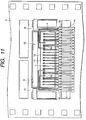
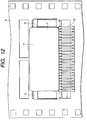
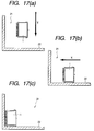
- FIG. 1 is a top view illustrating an electronic apparatus practiced as one preferred embodiment of the present invention.
- FIG. 2 is a side view illustrating the electronic apparatus shown in FIG. 1.
- the above-mentioned electronic apparatus is a dual in-line memory module (DIMM) for use as a main memory of a note-size personal computer for example.
- this memory module comprises a wiring board 2 mounted on both sides thereof with a plurality of tape carrier packages (TCPs) 1 and a case 3 for accommodating the wiring board 2.
- TCPs tape carrier packages
- the case 3 is provided at one part thereof with a slit 19 for letting the heat generated in the TCP 1 escape outside.
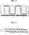
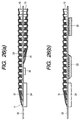
- FIG. 3 is a top view illustrating the top surface of the wiring board 2 with the TCP 1 mounted.
- FIG. 4 is a top view illustrating the rear surface of the wiring board 2 with the TCP 1 mounted.
- FIG. 5 is a side view illustrating a short side of the wiring board 2 with the TCP 1 mounted.
- Each of these TCPs 1 encapsulates a semiconductor chip (not shown) formed with a 16-megabit (Mbit) DRAM (Dynamic Random Access Memory) for example.
- Mbit 16-megabit
- DRAM Dynamic Random Access Memory
- One of the long sides of the wiring board 2 provides a connector.
- the connector is arranged on the top and rear sides thereof with a plurality of terminals (connector pins) 5 in a row for inserting this memory module into a socket of the mother board.
- the wiring board 2 is mounted in an excess area thereof with small electronic parts 6 and 7 such as a chip capacitor and a clock generator as required.
- the 32 TCPs 1 mounted on the wiring board 2 are all of the same dimensions. These TCPs 1 are all mounted at a small tilt angle of about 8 degrees relative to the mounting surface. In this mounting structure, the total thickness of the wiring board 2 including the TCPs 1 on both the sides is extremely small, complying with the strict memory module specifications in height (a maximum total height of 3.8 mm).
- each TCP 1 is mounted at a small tilt angle not more than 45 degrees, so that the surface area of each of these three TCPs 1 not covered by the adjacent TCP 1 increases, thereby enhancing heat dissipation of the densely mounted TCPs 1.
- a slight gap S is provided in the overlapped portion between adjacent TCPs 1 along the short direction of the wiring board 2. That is, these TCPs 1 are mounted such that each does not come in contact with the other.
- This mounting structure facilitates the air convection in the gap between the adjacent TCPs 1 mounted in a tilted relation to the mounting surface of the wiring board 2, further enhancing heat dissipation of the densely mounted TCPs 1.
- the TCPs 1 in the left-most row and the third row from the left end of the wiring board are arranged such that their leads 4 come to the top of the wiring board.
- the TCPs 1 in the second and fourth rows from the left end of the wiring board are arranged such that their leads 4 come to the bottom (the connector side) of the wiring board.
- the four rows of TCPs 1 arranged along the long side of the wiring board 2 are mounted such that each row alternates 180 degrees to the other in the mounting surface.
- the above-mentioned mounting structure allows the wiring of groups of wires for interconnecting the same pins of the two adjacent rows of TCPs 1 along the long side of the wiring board 2 without intersecting the wiring groups within the same mounting surface. Consequently, the number of wires to be laid from one side of the wiring board 2 to the other by way of through-holes is reduced as compared with the mounting in which the 16 TCPs 1 are arranged in the same direction. This arrangement in turn reduces the number of through-holes and the length of wiring, thereby realizing the high-density mounting of many TCPs 1 on the wiring board 2 limited in mounting area.
- the TCP 1 mounted on one side of the wiring board 2 and the TCP 1 mounted on the other side in an opposite manner are arranged such that the leads 4 of these TCPs 1 are directed in the opposite directions (to the left side and the right side in the figure).
- the pins of the TCPs 1 which are opposed to each other with the wiring board 2 sandwiched in are directed in the same direction. Consequently, the number of wires to be laid from one side of the wiring board 2 to the other by way of through-holes is reduced as compared with the mounting structure in which the TCPs 1 mounted on both sides of the wiring board 2 are directed in the same direction. This in turn reduces the number of through-holes and the length of wiring, thereby realizing the high-density mounting of many TCPs 1 on the wiring board 2 limited in mounting area.
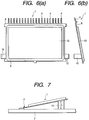
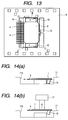
- the TCP 1 has an insulating tape 8, the plurality of leads 4 arranged on one side of the tape, a potting resin 9 for encapsulating a semiconductor chip 13, and a pair of support leads 10 arranged at two opposite short sides.
- support leads 10 function to hold the TCP 1 to a constant tilt angle relative to the mounting surface of the wiring board 2. Varying distance (L) vertical to the mounting surface allows the TCP 1 to be mounted at a desired tilt angle.
- the insulating tape 8 formed with the leads 4 and the pair of support leads 10 on one side is prepared at the outset. It should be noted that the insulating tape 8, which is usually long, is shown only in its part (for carrying only a single TCP).
- the insulating tape 8 is formed by a polyimide resin for example.
- the leads 4 and the pair of support leads 10 are formed by etching a metal foil such as a rolled copper foil laminated on one side of the insulating tape 8.
- One end (the tip of the inner lead portion 4a) of each lead 4 extends into inside a device hole 12 in which the semiconductor chip is arranged.
- the base end portion 4b of the outer lead portion 4c of each lead 4 is wider than the other portion of the outer lead to prevent the potting resin 9 from trailing (in the direction of the tip of the outer lead 4c), reinforce the leads 4, and prevent the same from being delaminated.
- the support lead 10 is bent halfway toward the short side by an angle ( ⁇ ) relative to the long side of the TCP 1. Adjusting the bend angle ( ⁇ ) in this portion determines the tilt angle ( ⁇ ) at which the TCP 1 is mounted on the wiring board 2. In the present embodiment, this bend angle ( ⁇ ) is set to about 8 degrees.
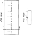
- a semiconductor chip 13 as shown in FIG. 10A is prepared.
- the semiconductor chip 1 is formed on the main surface thereof with a 16-megabit DRAM.
- a plurality of bonding pads 14 are also formed on the main surface of the semiconductor chip 13 in the center area of the chip along its long side.
- a gold (Au) bump electrode 14a for electrically connecting the tip of the inner lead 4a to the pad 14 is connected to each bonding pad 14 on the surface thereof as shown in FIG. 14B.
- the semiconductor chip 13 is positioned inside the device hole 12 of the insulating tape 8 as shown in FIG. 11. Then, the bonding pad 14 of the semiconductor chip 13 is electrically connected to the corresponding inner lead portion 4a at one end portion through the Au bump electrode 14a by use of a known inner lead bonder, not shown.
- the main surface side of the semiconductor chip including the junction between bonding pad 14 of the semiconductor chip 13 and the lead 4a is encapsulated with the potting resin 9 of epoxy type.
- each lead 4 the support lead 10, and a part of the insulating tape 8 are cut at the positions indicated by thick lines (A to F) shown in FIG. 13, the support lead 10 is bent at halfway thereof by 90 degrees, and the outer lead portion 4c of the lead 4 is bent into the shape as shown in FIG. 6B by use of a known cutting and forming die (not shown). Thus, the TCP 1 is completed.
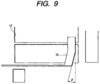
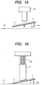
- the TCP 1 horizontally accommodated beforehand in a pocket 11a of a tray 11 as shown in FIG. 14A is held by a vacuum nozzle 17 and placed on a positioning stage 21 shown in FIG. 15.
- the tip of the vacuum nozzle 17 is constituted by a soft member such as a rubber or soft resin for example and a load mitigating mechanism for making this tip portion vertically movable by use of a spring 17a is provided on the vacuum nozzle 17.
- These provisions prevent the lead 4 and the support lead 10 from being deformed by the weight of the vacuum nozzle 17 when the TCP 1 is brought down into intimate contact with the positioning stage 21 by the vacuum nozzle 17.
- the vacuum nozzle 17 is provided at the bottom thereof with a tilt of the same angle (about 8 degrees) as the tilt angle of the TCP 1 as shown, allowing the TCP 1 to be vacuum-held with the tilt angle kept unchanged.
- the positioning stage on which the TCP 1 is placed is moved in X and Y directions to position the TCP 1 to the reference point of a square fixing jig 22. Then, the TCP 1 is held by the vacuum nozzle 17 again to be carried to a predetermined position on the wiring board 2 according to predetermined positional information.
- the lead 4 of the TCP 1 is temporarily attached to a foot print 18 of the wiring board 2 with solder paste printed beforehand. The solder is reflowed with the tilt angle of the TCP 1 relative to the mounting surface kept constant by the support lead 10 to solder the lead 4 to the foot print 18.
- a bent 4d as shown in the figure is provided halfway along the lead 4 to pool the solder, thereby preventing the same from creeping up to the base end portion 4b.
- this bent 4d acts to mitigate or absorb a stress applied to the lead 4 by means of the deformation of the bent, thereby preventing the lead 4 from being broken.
- the support lead 10 When mounting the TCP 1 on the wiring board 2, the support lead 10 is not fixed to the wiring board 2. By doing so, if the TCP 1 mounted so that a part thereof gets under an adjacent TCP 1a fails after mounting, the adjacent TCP 1 may be lifted around the junction between the wiring board 2 and the lead 4 as shown in FIG. 20 to replace the failing TCP 1 with ease. Also, when mounting the TCP 1 on the wring board 2, small electronic parts (6, 7) such as the chip capacitor and an LSI package of planar mounting type such as a CSP (Chip Size Package) are mounted as required at the same time.
- small electronic parts (6, 7) such as the chip capacitor and an LSI package of planar mounting type such as a CSP (Chip Size Package) are mounted as required at the same time.
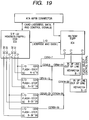
- FIG. 19 is a circuit diagram of the memory module practiced as the above-mentioned embodiment of the invention.
- the case 3 for accommodating the wiring board 2 is formed by punching a thin metal sheet having a high thermal conductivity such as aluminum (Al), folding the resultant thin metal sheet into two parts, and inserting the wiring board 2 between the these parts.
- This structure prevents the TCPs 1 mounted on the wiring board 2 from being deformed.
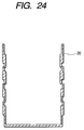
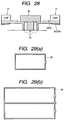
- a resin sheet shaped as shown in FIG. 24 may be inserted between the TCPs 1 mounted on the wiring board 2 as a spacer 20 as shown in FIGS. 22 and 23.
- This arrangement enhances the mechanical strength of the memory module, thereby preventing the TCPs 1 from being deformed by a strong force that is applied to the case 3 when the memory module is inserted in the socket of a mother board.
- the spacer 20 is fixed to the wiring board 2 by means of an adhesive or mechanical insertion.
- An electronic apparatus practiced as a second preferred embodiment of the invention is a memory card for use as an external auxiliary storage device for a note-size personal computer for example.
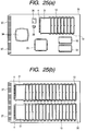
- FIG. 25A is a top view illustrating the front side of a wiring board to be accommodated in this memory card.
- FIG. 25B is a top view illustrating the rear side of this wiring board.
- FIG. 26A is a side view illustrating one long side of this wiring board.
- FIG. 26B is a side view illustrating the other long side of the wiring board. It should be noted that a case for accommodating the wiring board is not shown.
- TCPs 31 are mounted in a row on the front surface of the wiring board 30.
- 32 TCPs 31 are mounted in two rows (a total of 40 TCPs 31 on both sides).
- a semiconductor chip (not shown) formed with a 64-megabit (Mbit) flash memory for example is encapsulated.
- Each TCP 31 is electrically connected to the wiring board 30 through a plurality of leads 4 arranged in a row along one side of the TCP 31.
- the other portions of the front surface of the wiring board 30 are arranged with a decoder 32, a microcomputer 33, an interface circuit 34, a TTL 35 for reset signal generation, and a clock module 36.
- the interface circuit 34 is of a chip-on-board (COB) structure and can be constituted by a planar mount type package such as a chip size package (CSP).
- COB chip-on-board
- CSP chip size package
- One of the short sides of the wiring board 30 is a connector that is arranged on the front and rear sides thereof with a plurality of terminals (connector pins) 37 in a row.
- the 40 TCPs 31 mounted on the wiring board 2 are all of the same dimensions. As shown in FIGS. 26A and 26B, each TCP 31 is mounted with a small tilt angle to the mounting surface. The tilt angle is adjustable by means of the support lead 10 in the same manner as the TCP 1 of the first embodiment. Except for the TCP 31 arranged at one end of the wiring board, the TCPs 31 are mounted such that a portion of each gets under the adjacent one. The overlapped portion is provided a slight gap in between.
- the above-mentioned mounting structure keeps extremely small the thickness (or height) of the wiring board 30 mounted on both sides with the TCPs 31, complying with the memory card standards strict in height specification (a maximum of 5 mm).
- the above-mentioned mounting structure also realizes the high-density mounting of many TCPs 31 on the wiring board 30 limited in mounting dimensions.
- the TCP 31 may be fabricated and mounted on the wiring board 30 in generally the same manner as described with respect to the above-mentioned preferred embodiment 1.
- spacers 38 and 39 as shown in FIGS. 29A and 29B are inserted into a gap of the TCPs 31 to enhance the mechanical strength of the memory card.
- the spacer 38 is arranged around the 8 TCPs 31 mounted on the front surface of the wiring board 30.
- the spacer 39 is arranged around the 32 TCPs 31 mounted on the rear surface of the wiring board 30.
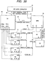
- FIG. 30 is a circuit diagram illustrating the memory card of the second embodiment fabricated as described above.
- the memory card described with reference to FIGS. 25 through 29 constitutes an ATA (AT Attachment) card system shown in FIG. 30 for example.
- the ATA card complies with the interface and protocol to be used by an AT-compatible computer for accessing a hard disk drive.
- This card is standardized by the standardizing organization of PCMCIA (Personal Computer Memory Card International Association).
- Reference numeral 40 denotes the pin connector of the ATA card that corresponds to an external terminal 37.
- the ATA card transfers signals with a PC (Personal Computer) or a PDA (Personal Digital Assistant).
- PCMCIA Personal Computer Card
- a gate array GA 34 Externally supplied data and addresses are inputted in a gate array GA 34 through a signal line 41.
- the gate array GA controls an external PCMCIA interface, a microcomputer MPU 33, a flash memory FM 31, and the data transfer between the flash memory FM 31 and the PCMCIA interface.
- the transfer of data and addresses between elements in the card is performed through a local data bus and a local address bus referenced at 42.
- the MPU 33 receives an externally supplied command 44 to perform data control. Externally supplied data is sent to the flash memory FM 31 through a decoder DC for high-speed data processing for both read and write operations. Selection of the flash memory FM 31 for data writing and data reading is controlled by a CEN (Chip Enable) bus 43. Further, to enhance the reliability of the data stored in the flash memory FM 31, the MPU 33 performs ECC (Error Check and Correction) (for controlling the count of rewriting of each section and controlling access to failing sectors) and wear leveling (averaging the count of rewriting failing sectors).
- ECC Error Check and Correction
Landscapes
- Engineering & Computer Science (AREA)
- Manufacturing & Machinery (AREA)
- Microelectronics & Electronic Packaging (AREA)
- Wire Bonding (AREA)
- Structures For Mounting Electric Components On Printed Circuit Boards (AREA)
- Lead Frames For Integrated Circuits (AREA)
- Combinations Of Printed Boards (AREA)
- Multi-Conductor Connections (AREA)
Applications Claiming Priority (2)
| Application Number | Priority Date | Filing Date | Title |
|---|---|---|---|
| JP34787197A JP3718039B2 (ja) | 1997-12-17 | 1997-12-17 | 半導体装置およびそれを用いた電子装置 |
| JP34787197 | 1997-12-17 |
Publications (2)
| Publication Number | Publication Date |
|---|---|
| EP0924764A2 true EP0924764A2 (fr) | 1999-06-23 |
| EP0924764A3 EP0924764A3 (fr) | 2000-03-08 |
Family
ID=18393168
Family Applications (1)
| Application Number | Title | Priority Date | Filing Date |
|---|---|---|---|
| EP98121912A Withdrawn EP0924764A3 (fr) | 1997-12-17 | 1998-11-18 | Carte de circuit imprimé avec une pluralité de dispositifs sémiconducteurs |
Country Status (7)
| Country | Link |
|---|---|
| US (1) | US6169325B1 (fr) |
| EP (1) | EP0924764A3 (fr) |
| JP (1) | JP3718039B2 (fr) |
| KR (1) | KR19990063110A (fr) |
| CN (1) | CN1220492A (fr) |
| SG (1) | SG74680A1 (fr) |
| TW (1) | TW459365B (fr) |
Cited By (3)
| Publication number | Priority date | Publication date | Assignee | Title |
|---|---|---|---|---|
| WO2002041398A3 (fr) * | 2000-11-16 | 2003-04-10 | Unitive Electronics Inc | Boitiers micro-electronique et procedes d'encapsulation dans lesquels des seconds substrats micro-electroniques sont orientes par rapport a des premiers substrats micro-electroniques pour former un angle aigu |
| EP1333443A1 (fr) * | 2002-01-31 | 2003-08-06 | Infineon Technologies AG | Système de mémoire |
| EP1471778A1 (fr) * | 2003-04-24 | 2004-10-27 | Infineon Technologies AG | Module de mémoire ayant un arrangement peu encombrant des puces mémoire et par consequent la puce mémoire |
Families Citing this family (41)
| Publication number | Priority date | Publication date | Assignee | Title |
|---|---|---|---|---|
| KR100335716B1 (ko) * | 2000-05-23 | 2002-05-08 | 윤종용 | 메모리 카드 |
| US6396711B1 (en) * | 2000-06-06 | 2002-05-28 | Agere Systems Guardian Corp. | Interconnecting micromechanical devices |
| US6760229B2 (en) * | 2000-10-18 | 2004-07-06 | Hewlett-Packard Development Company, L.P. | System for protecting electronic components |
| DE60108413T2 (de) * | 2000-11-10 | 2005-06-02 | Unitive Electronics, Inc. | Verfahren zum positionieren von komponenten mit hilfe flüssiger antriebsmittel und strukturen hierfür |
| US6863209B2 (en) | 2000-12-15 | 2005-03-08 | Unitivie International Limited | Low temperature methods of bonding components |
| JP2002204053A (ja) * | 2001-01-04 | 2002-07-19 | Mitsubishi Electric Corp | 回路実装方法、回路実装基板及び半導体装置 |
| KR100380107B1 (ko) * | 2001-04-30 | 2003-04-11 | 삼성전자주식회사 | 발열체를 갖는 회로 기판과 기밀 밀봉부를 갖는 멀티 칩패키지 |
| US6433413B1 (en) | 2001-08-17 | 2002-08-13 | Micron Technology, Inc. | Three-dimensional multichip module |
| US6747347B2 (en) * | 2001-08-30 | 2004-06-08 | Micron Technology, Inc. | Multi-chip electronic package and cooling system |
| US6686654B2 (en) * | 2001-08-31 | 2004-02-03 | Micron Technology, Inc. | Multiple chip stack structure and cooling system |
| KR100429878B1 (ko) * | 2001-09-10 | 2004-05-03 | 삼성전자주식회사 | 메모리 모듈과 그에 사용되는 인쇄회로기판 |
| US6751113B2 (en) * | 2002-03-07 | 2004-06-15 | Netlist, Inc. | Arrangement of integrated circuits in a memory module |
| US7531898B2 (en) * | 2002-06-25 | 2009-05-12 | Unitive International Limited | Non-Circular via holes for bumping pads and related structures |
| US6960828B2 (en) * | 2002-06-25 | 2005-11-01 | Unitive International Limited | Electronic structures including conductive shunt layers |
| US7547623B2 (en) * | 2002-06-25 | 2009-06-16 | Unitive International Limited | Methods of forming lead free solder bumps |
| JP3920195B2 (ja) * | 2002-11-11 | 2007-05-30 | 新光電気工業株式会社 | 電子部品実装構造及びその製造方法 |
| TWI225899B (en) * | 2003-02-18 | 2005-01-01 | Unitive Semiconductor Taiwan C | Etching solution and method for manufacturing conductive bump using the etching solution to selectively remove barrier layer |
| US7049216B2 (en) * | 2003-10-14 | 2006-05-23 | Unitive International Limited | Methods of providing solder structures for out plane connections |
| KR100513422B1 (ko) | 2003-11-13 | 2005-09-09 | 삼성전자주식회사 | 집적회로 모듈의 구조 |
| US7358174B2 (en) | 2004-04-13 | 2008-04-15 | Amkor Technology, Inc. | Methods of forming solder bumps on exposed metal pads |
| JP4674477B2 (ja) * | 2005-03-03 | 2011-04-20 | パナソニック株式会社 | 半導体モジュール |
| US20060205170A1 (en) * | 2005-03-09 | 2006-09-14 | Rinne Glenn A | Methods of forming self-healing metal-insulator-metal (MIM) structures and related devices |
| DE102005051497B3 (de) * | 2005-10-26 | 2006-12-07 | Infineon Technologies Ag | Speichermodul mit einer elektronischen Leiterplatte und einer Mehrzahl von gleichartigen Halbleiterchips |
| DE102005051998B3 (de) * | 2005-10-31 | 2007-01-11 | Infineon Technologies Ag | Halbleiterspeichermodul |
| US7674701B2 (en) | 2006-02-08 | 2010-03-09 | Amkor Technology, Inc. | Methods of forming metal layers using multi-layer lift-off patterns |
| US7932615B2 (en) * | 2006-02-08 | 2011-04-26 | Amkor Technology, Inc. | Electronic devices including solder bumps on compliant dielectric layers |
| KR100715287B1 (ko) * | 2006-04-26 | 2007-05-08 | 삼성전자주식회사 | 반도체 메모리 모듈 |
| JP4116055B2 (ja) * | 2006-12-04 | 2008-07-09 | シャープ株式会社 | 半導体装置 |
| US7443694B1 (en) * | 2006-12-14 | 2008-10-28 | Sun Microsystems, Inc. | 25 degree tool-less expansion card bracket |
| EP2378911B1 (fr) * | 2008-11-21 | 2014-05-21 | Boa Technology, Inc. | Système de laçage a enrouleur |
| US8553420B2 (en) | 2010-10-19 | 2013-10-08 | Tessera, Inc. | Enhanced stacked microelectronic assemblies with central contacts and improved thermal characteristics |
| US9013033B2 (en) | 2011-04-21 | 2015-04-21 | Tessera, Inc. | Multiple die face-down stacking for two or more die |
| US8928153B2 (en) | 2011-04-21 | 2015-01-06 | Tessera, Inc. | Flip-chip, face-up and face-down centerbond memory wirebond assemblies |
| US8970028B2 (en) | 2011-12-29 | 2015-03-03 | Invensas Corporation | Embedded heat spreader for package with multiple microelectronic elements and face-down connection |
| US8952516B2 (en) | 2011-04-21 | 2015-02-10 | Tessera, Inc. | Multiple die stacking for two or more die |
| US8633576B2 (en) | 2011-04-21 | 2014-01-21 | Tessera, Inc. | Stacked chip-on-board module with edge connector |
| JP6500885B2 (ja) * | 2016-12-20 | 2019-04-17 | 日亜化学工業株式会社 | 発光装置の製造方法 |
| US9893037B1 (en) * | 2017-04-20 | 2018-02-13 | Nanya Technology Corporation | Multi-chip semiconductor package, vertically-stacked devices and manufacturing thereof |
| US11387054B2 (en) | 2018-02-22 | 2022-07-12 | KYOCERA AVX Components Corporation | Electrical circuit including a supercapacitor with reduced leakage |
| US10734358B2 (en) * | 2018-06-14 | 2020-08-04 | Intel Corporation | Multi-packaging for single-socketing |
| WO2023076900A1 (fr) * | 2021-10-27 | 2023-05-04 | Atieva, Inc. | Agencement non plan de puces de puissance pour gestion thermique |
Family Cites Families (12)
| Publication number | Priority date | Publication date | Assignee | Title |
|---|---|---|---|---|
| JP2509969B2 (ja) * | 1988-02-26 | 1996-06-26 | 株式会社日立製作所 | 電子装置 |
| US5227664A (en) * | 1988-02-26 | 1993-07-13 | Hitachi, Ltd. | Semiconductor device having particular mounting arrangement |
| USRE36325E (en) * | 1988-09-30 | 1999-10-05 | Micron Technology, Inc. | Directly bonded SIMM module |
| US5057907A (en) * | 1990-06-11 | 1991-10-15 | National Semiconductor Corp. | Method and structure for forming vertical semiconductor interconnection |
| JPH0465135A (ja) | 1990-07-05 | 1992-03-02 | Matsushita Electric Ind Co Ltd | 半導体装置およびその実装構造体 |
| US5239447A (en) * | 1991-09-13 | 1993-08-24 | International Business Machines Corporation | Stepped electronic device package |
| US5343366A (en) * | 1992-06-24 | 1994-08-30 | International Business Machines Corporation | Packages for stacked integrated circuit chip cubes |
| AU4857493A (en) * | 1992-09-16 | 1994-04-12 | James E. Clayton | A thin multichip module |
| US5731633A (en) * | 1992-09-16 | 1998-03-24 | Gary W. Hamilton | Thin multichip module |
| JPH07321441A (ja) | 1994-05-24 | 1995-12-08 | Hitachi Ltd | 電子回路装置 |
| JP2655118B2 (ja) | 1995-01-10 | 1997-09-17 | 日本電気株式会社 | 半導体装置 |
| US5766982A (en) * | 1996-03-07 | 1998-06-16 | Micron Technology, Inc. | Method and apparatus for underfill of bumped or raised die |
-
1997
- 1997-12-17 JP JP34787197A patent/JP3718039B2/ja not_active Expired - Fee Related
-
1998
- 1998-11-18 EP EP98121912A patent/EP0924764A3/fr not_active Withdrawn
- 1998-11-19 TW TW087119198A patent/TW459365B/zh not_active IP Right Cessation
- 1998-12-07 SG SG1998005254A patent/SG74680A1/en unknown
- 1998-12-15 US US09/210,883 patent/US6169325B1/en not_active Expired - Lifetime
- 1998-12-16 KR KR1019980055411A patent/KR19990063110A/ko not_active Withdrawn
- 1998-12-17 CN CN98125582A patent/CN1220492A/zh active Pending
Cited By (4)
| Publication number | Priority date | Publication date | Assignee | Title |
|---|---|---|---|---|
| WO2002041398A3 (fr) * | 2000-11-16 | 2003-04-10 | Unitive Electronics Inc | Boitiers micro-electronique et procedes d'encapsulation dans lesquels des seconds substrats micro-electroniques sont orientes par rapport a des premiers substrats micro-electroniques pour former un angle aigu |
| EP1333443A1 (fr) * | 2002-01-31 | 2003-08-06 | Infineon Technologies AG | Système de mémoire |
| EP1471778A1 (fr) * | 2003-04-24 | 2004-10-27 | Infineon Technologies AG | Module de mémoire ayant un arrangement peu encombrant des puces mémoire et par consequent la puce mémoire |
| US7061089B2 (en) | 2003-04-24 | 2006-06-13 | Infineon Technologies Ag | Memory module having space-saving arrangement of memory chips and memory chip therefore |
Also Published As
| Publication number | Publication date |
|---|---|
| JP3718039B2 (ja) | 2005-11-16 |
| KR19990063110A (ko) | 1999-07-26 |
| SG74680A1 (en) | 2000-08-22 |
| JPH11186489A (ja) | 1999-07-09 |
| TW459365B (en) | 2001-10-11 |
| CN1220492A (zh) | 1999-06-23 |
| EP0924764A3 (fr) | 2000-03-08 |
| US6169325B1 (en) | 2001-01-02 |
Similar Documents
| Publication | Publication Date | Title |
|---|---|---|
| US6169325B1 (en) | Semiconductor device | |
| US9377825B2 (en) | Semiconductor device | |
| KR101075360B1 (ko) | 집적 회로 스택 쌓기 집적 회로 패키지 및 그 제조 방법 | |
| US5723903A (en) | Thin type semiconductor device, module structure using the device and method of mounting the device on board | |
| US6492737B1 (en) | Electronic device and a method of manufacturing the same | |
| US6900530B1 (en) | Stacked IC | |
| JPH01217996A (ja) | 電子装置 | |
| US6121681A (en) | Semiconductor device | |
| JPH11135670A (ja) | ボールグリッドアレイパッケージ | |
| KR100281056B1 (ko) | 반도체장치및반도체장치모듈 | |
| CN100490609C (zh) | 组件及电气封装 | |
| US20040130036A1 (en) | Mult-chip module | |
| US20050189626A1 (en) | Semiconductor device support structures | |
| US6469903B1 (en) | Flexible printed circuit and semiconductor device | |
| US20050104206A1 (en) | Mounting structure in integrated circuit module | |
| CN110416169B (zh) | 半导体模块 | |
| JP4402806B2 (ja) | 半導体装置 | |
| JP3904296B2 (ja) | メモリシステム | |
| JP3288973B2 (ja) | 半導体装置、積層体及びモジュール構造体 | |
| US8491982B2 (en) | Apparatus for manufacturing bonding structure, bonding structure and method of fabricating the same | |
| JP2811757B2 (ja) | Icメモリカード | |
| KR0163307B1 (ko) | 고밀도 실장용 반도체 칩 패키지 | |
| JPH0851180A (ja) | 半導体装置 | |
| US7265446B2 (en) | Mounting structure for semiconductor parts and semiconductor device | |
| JP3320017B2 (ja) | モジュール構造体 |
Legal Events
| Date | Code | Title | Description |
|---|---|---|---|
| PUAI | Public reference made under article 153(3) epc to a published international application that has entered the european phase |
Free format text: ORIGINAL CODE: 0009012 |
|
| AK | Designated contracting states |
Kind code of ref document: A2 Designated state(s): AT BE CH CY DE DK ES FI FR GB GR IE IT LI LU MC NL PT SE |
|
| AX | Request for extension of the european patent |
Free format text: AL;LT;LV;MK;RO;SI |
|
| PUAL | Search report despatched |
Free format text: ORIGINAL CODE: 0009013 |
|
| AK | Designated contracting states |
Kind code of ref document: A3 Designated state(s): AT BE CH CY DE DK ES FI FR GB GR IE IT LI LU MC NL PT SE |
|
| AX | Request for extension of the european patent |
Free format text: AL;LT;LV;MK;RO;SI |
|
| AKX | Designation fees paid | ||
| STAA | Information on the status of an ep patent application or granted ep patent |
Free format text: STATUS: THE APPLICATION IS DEEMED TO BE WITHDRAWN |
|
| 18D | Application deemed to be withdrawn |
Effective date: 20000909 |