EP0924765A2 - Speicher mit gesteuerter Wortleitungsspannung - Google Patents
Speicher mit gesteuerter Wortleitungsspannung Download PDFInfo
- Publication number
- EP0924765A2 EP0924765A2 EP98120100A EP98120100A EP0924765A2 EP 0924765 A2 EP0924765 A2 EP 0924765A2 EP 98120100 A EP98120100 A EP 98120100A EP 98120100 A EP98120100 A EP 98120100A EP 0924765 A2 EP0924765 A2 EP 0924765A2
- Authority
- EP
- European Patent Office
- Prior art keywords
- voltage
- transistor
- turn
- row
- conduction path
- Prior art date
- Legal status (The legal status is an assumption and is not a legal conclusion. Google has not performed a legal analysis and makes no representation as to the accuracy of the status listed.)
- Granted
Links
Images



Classifications
-
- G—PHYSICS
- G11—INFORMATION STORAGE
- G11C—STATIC STORES
- G11C11/00—Digital stores characterised by the use of particular electric or magnetic storage elements; Storage elements therefor
- G11C11/21—Digital stores characterised by the use of particular electric or magnetic storage elements; Storage elements therefor using electric elements
- G11C11/34—Digital stores characterised by the use of particular electric or magnetic storage elements; Storage elements therefor using electric elements using semiconductor devices
- G11C11/40—Digital stores characterised by the use of particular electric or magnetic storage elements; Storage elements therefor using electric elements using semiconductor devices using transistors
- G11C11/401—Digital stores characterised by the use of particular electric or magnetic storage elements; Storage elements therefor using electric elements using semiconductor devices using transistors forming cells needing refreshing or charge regeneration, i.e. dynamic cells
- G11C11/4063—Auxiliary circuits, e.g. for addressing, decoding, driving, writing, sensing or timing
- G11C11/407—Auxiliary circuits, e.g. for addressing, decoding, driving, writing, sensing or timing for memory cells of the field-effect type
- G11C11/408—Address circuits
- G11C11/4085—Word line control circuits, e.g. word line drivers, - boosters, - pull-up, - pull-down, - precharge
-
- G—PHYSICS
- G11—INFORMATION STORAGE
- G11C—STATIC STORES
- G11C8/00—Arrangements for selecting an address in a digital store
- G11C8/08—Word line control circuits, e.g. drivers, boosters, pull-up circuits, pull-down circuits, precharging circuits, for word lines
-
- H—ELECTRICITY
- H10—SEMICONDUCTOR DEVICES; ELECTRIC SOLID-STATE DEVICES NOT OTHERWISE PROVIDED FOR
- H10B—ELECTRONIC MEMORY DEVICES
- H10B12/00—Dynamic random access memory [DRAM] devices
- H10B12/50—Peripheral circuit region structures
Definitions
- This invention relates to memory devices such as dynamic random access memories (DRAMs) and, in particular, to a method and apparatus for sensing and/or controlling certain leakage currents associated with memory cells of the DRAM.
- DRAMs dynamic random access memories
- Fig. 1 shows a memory array 10 comprised of memory cells 11.
- the array 10 is shown to have M rows, with one row conductor or word line (WL) per row and to have N columns, with one column conductor or bit line (BL) per column.
- a memory cell 11 is located at the intersection of each row and column conductor.
- the row conductors, or word lines are driven by a row decoder and driver circuit 20 and the column conductors, or bit lines, are driven by a column decoder and driver circuit 30.
- a write/sense circuit 40 includes circuitry for writing information onto the bit lines for transmission to selected memory cells and circuitry to sense information read from selected memory cells and coupled onto the bit lines.
- a word line is activated (selected or enabled) by the application thereto of a "high" voltage (e.g., VDD volts) and the word line is deactivated (not-selected, disabled or in stand-by condition) by the application thereto of a "low" voltage (e.g., zero volts).
- a "high" voltage e.g., VDD volts
- a "low" voltage e.g., zero volts
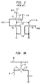
- the M word lines of the array 10 are selectively enabled by means of row driver circuit 20 which has M decoder/driver circuits, each of which may be of the type shown in FIG. 2.
- the decoder driver of FIG.2 includes a P type transistor, P1, having its source-to-drain path connected between a signal terminal 211 and an output terminal 213 to which is connected its associated word line (WL).
- the substrate 212 of P1 is connected to a terminal 214 to which is applied a fixed potential (e.g., VDD volts).
- the source-to-drain paths of transistors N1 and N2 are connected in parallel between output terminal 213, which is connected to a word line (WL), and a terminal 216 to which is applied ground potential.
- a first partially decoded signal, RDEC, is applied to the gates of transistors P1 and N1 and a second partially decoded signal, WLD, is applied to signal terminal 211.
- a signal WLK (typically the inverse of WLD) is applied to the gate of N2 to enable the word line to be selectively clamped to ground for certain input signal conditions.
- the circuit of FIG. 2 is used to activate a selected word line.
- a "high” is applied to the word line, activating it and enabling the memory cell transistors whose gates are connected to the word line.
- a "low” e.g., ground
- the circuit of FIG. 2 may be used to apply either an activation (turn-on) voltage (e.g., VDD volts) to the word lines or a deactivation (turn-off) voltage (e.g., zero volts) to the word lines.
- the ability to apply a single fixed turn-off voltage is unsatisfactory in certain applications. This is best explained by noting that the memory cells of DRAMs are subject to leakage currents which can destroy the data stored in the memory cells of the DRAM. Therefore, it is necessary to test the cells of a memory array to ensure that their leakage is within acceptable limits. Where, for example, the memory cell transistors are of N-conductivity type, the testing is normally done by first activating the word lines of the memory array by applying a high voltage to them and writing a "high" into the cells by charging their storage capacitors to a high voltage. The word lines are then deactivated by applying zero volts to the word lines for a known period of time.
- the memory cells are selectively read out to determine their data retention.
- a word line is deactivated a single, fixed, turn-off voltage of, for example, zero volts is applied to a word line when it is deselected.
- GIDL gate induced drain leakage
- Applicant's invention resides, in part, in the recognition that it may be desirable and/or necessary to test, or operate, a memory array by applying different values of turn-off voltages to the word lines of a memory array.
- Applicant recognized that it is desirable to test the leakage of memory cell transistors by applying turn-off voltages to their gates which exceed in amplitude and polarity the normal turn-off voltage applied to their gates.
- Applicant also recognized that it may be desirable and/or necessary to make a memory array which includes circuitry to enable different turn-off voltages to be applied to the word lines of the memory array.
- Applicant's invention also resides in circuitry for applying either a normal turn-off voltage (e.g., zero volts for an N-type transistor) or a greater than normal (e.g., - 1 volt for an N-type transistor) turn-off voltage to the gates of memory cell transistors.
- a normal turn-off voltage e.g., zero volts for an N-type transistor
- a greater than normal e.g., - 1 volt for an N-type transistor
- Memory systems embodying the invention include circuitry for applying a first turn-off voltage to selected word lines for turning-off current conduction in the main conduction path of the memory cell transistors whose gates are connected to these word lines and for selectively applying an increased turn-off voltage to selected word lines for more sharply turning-off the memory cell transistors whose gates are connected to these word lines.
- turn-off voltages ranging in value are applied to the word lines to test the susceptibility of the memory cells to gate induced drain leakage (GIDL) current.
- GIDL gate induced drain leakage
- For a further increase in the turn-off voltage applied to the word lines the leakage current of the transistors whose gates are connected to the word lines increases. Determining the range of turn-off voltage for which the leakage is a minimum and the range for which the leakage increases may be used to set the limit of the amplitude of turn-off voltage and to select an appropriate range of turn-off voltages.
- the turn-off voltages tending to increase the leakage current may be used to test the susceptibility of the memory cell transistors to gate induced drain leakage (GIDL) currents. This testing enables the detection and correction or rejection of potentially defective memory products, thus leading to the manufacture of a more reliable product.
- GIDL gate induced drain leakage
- a method embodying the invention includes the steps of: (a) writing a certain signal condition (e.g., a High) to be stored in the memory cells of a memory array; (b) applying a first turn-off voltage for a first time period to selected word lines of the memory array; (c) sensing the contents of the memory cells to determine the effect, if any, of leakage currents with the first turn-off voltage on selected memory cells; (d) rewriting the certain signal condition in the memory array; (e) applying a second turn-off voltage for a period of time generally equal to said first time period; and (f) sensing the contents of the memory cells to determine the effect of leakage currents for the second value of turn-off voltage on the selected memory cells; and, wherein one of said first and second turn-off voltage is of greater amplitude than the other.
- a certain signal condition e.g., a High
- memory systems embodying the invention include circuits for testing the susceptibility of the memory cells to gate induced drain leakage (GIDL) as a function of turn-off voltage.
- the testing of the memory cells may be used to set the word line turn-off voltage and/or to replace defective rows and columns with redundant rows and columns, and/or reject defective memory arrays.
- GIDL gate induced drain leakage
- a memory cell 11 of the memory array 10 shown in FIG. 1 includes a transistor T1 and a storage capacitor C1.
- transistor (T1) has a gate electrode 13, which is connected to its associated word line (WL), a first electrode 14, which functions as source or drain, connected to its associated bit line (BL), and a second electrode 15, which also functions as a drain or source, connected to one end of a storage capacitor, C1.
- Fig. 3B is a cross-sectional diagram of the memory cell of Fig. 3A and shows that N-regions 14 and 15 are formed in a P-substrate 16.
- Regions 14 and 15 define the ends of the main conduction path in substrate 16.
- N region 14 also forms a PN junction with substrate 16 identified as "parasitic" diode D1
- N region 15 also forms a PN junction with substrate 16 identified as “parasitic” diode D2.
- These parasitic diodes, D1 and D2 may be the source of leakage as described below.
- Diodes D1 and D2 are normally operated in a reverse biased condition by maintaining the substrate voltage more negative than the voltages at the source drain regions 14 and 15.
- the substrate 16 is shown to be grounded. However, a small negative bias of Vbb volts (where Vbb is, for example, equal to -1 volt) may be applied to the substrate 16.
- Vbb is, for example, equal to -1 volt
- FIG. 3C is a schematic diagram of the memory cell of Fig. 3B including the parasitic diodes D1 and D2.
- the memory cell transistors (T1) are metal-oxide-semiconductor (MOS) transistors of N-conductivity type.
- MOS metal-oxide-semiconductor
- N-type transistors are used by way of example only and different types of transistors (e.g., P-type) could be used instead.
- an MOS transistor is a device having: (a) source and drain electrodes defining the ends of a main conduction path: and (b) a gate electrode overlying the main conduction path whose applied voltage controls the conductivity of the main conduction path.
- An N-type transistor is turned-on when its gate potential exceeds its source potential by more than the threshold voltage (Vt) of the transistor.
- the source electrode of the N-type transistor is defined as that one of the first and second electrodes having the lower potential applied thereto. Since an N-type transistor (as well as a P-type transistor) when operated as a gating transistor can conduct bidirectionally, which electrode is the source and which is the drain is a function of the potential applied to these electrodes.
- a logic "0” or a logic “1” can be written into and stored in a memory cell 11.
- the operating potential to the memory array is VDD volts (e.g., 5 volts) and ground (e.g., zero volts) it may be assumed, for purpose of illustration, that: (a) a logic "0” or low signal is a signal having a value of zero, or close to zero, volts; and (b) a logic "1" or high signal is a signal having a value of VDD, or close to VDD, volts.
- Information is written into a memory cell 11 when its gating transistor is enabled (e.g., turned-on by applying, for example, VDD volts to the WL connected to its gate 13).
- a logic zero can then be written into the memory cell by applying zero volts to the bit line connected to electrode 14.
- Capacitor C1 can then be discharged to ground via the drain-to-source path of transistor T1.
- T1 may then be turned off by the application of zero volts to the WL connected to its gate and C1 will remain at or close to zero volts.
- a logic "1" is written into a memory cell when its T1 is turned on, as noted above, and by applying VDD volts to the bit line connected to its drain electrode. Capacitor C1 gets charged up towards VDD via the source-drain conduction path of T1. T1 may then be turned off by the application of zero volts to its gate. Capacitor C1 will remain charged at the high potential ([VDD - Vt] volts) to which it was charged except for the presence of leakage currents which tend to discharge C1 to ground. For purpose of illustration assume that, when a logic "1" is written into a memory cell 11, the storage capacitor, C1, is charged to a voltage of for example +5 volts.
- the gate voltage of the memory cell transistor T1 is driven “low” (e.g. zero volts) to turn-off transistor T1.
- Transistor T1 will remain turned-off (i.e., in a "stand-by” condition) until a subsequent read, refresh or rewrite operation, with the expectation that capacitor C1 will remain charged to, or close to, +5 volts.
- the gate voltage of T1 is at zero while its drain is at +5 volts the gate is at a negative 5 volts relative to the drain. For extremely small sized transistors, this voltage induces a high electric field at the drain 15 to substrate 16 junction.
- FIG. 4 is an exemplary diagram showing the flow of current (IDS) in the main conduction path of a transistor as a function of gate voltage and the effect of increasing the turn-off voltage applied to the gate on the flow of leakage current (e.g., gate induced drain leakage, GIDL, current).
- IDS flow of current
- the leakage current (GIDL) through the parasitic diodes increases significantly, and particularly through D2 when the drain is positively biased by the charge on the storage capacitor.
- Applicant's invention resides, in part in the recognition that the leakage of transistors of the memory cells of a memory array could be tested for different values of turn-off voltages to determine how the leakage current varies as a function of increasing and decreasing values of turn-off voltages.
- these are voltages which make the gate of the transistor negative relative to its source.
- the testing enables the detection of the location of defective cells so that they can be replaced by cells from a redundant row or, column (not shown). Alternatively if there are too many defective cells, so that the redundant rows and columns are insufficient, the memory chip would be rejected.
- the testing also enables the determination of the optimum turn-off gate voltage or the optimum design of the memory transistors.
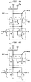
- Applicant's invention also resides in decoder circuitry such as shown in FIG. 5 which enables different voltages (e.g., ground or Vbb volts) to be selectively applied to selected word lines.
- Fig. 5 includes a transistor P1, as in FIG. 2, for selectively supplying a high voltage to the word line (WL).
- transistors N1 and N2 are formed in an isolated P-well, 51, to enable a negative bias voltage of Vbb volts to be connected to the P-well 51 at a terminal 52 thereof.
- Vbb may be, for example, equal to -1 volt. However, Vbb may be selected to be any voltage between Vt and -VA volts.
- the source electrodes 53s and 54s of N1 and N2 are connected to a node 41.
- the circuit of FIG. 5 enables the application of either ground or Vbb volts to node 41.
- Transistors N1 and N2, when enabled, function to couple whatever voltage is present at node 41 to the word line (WL).
- the source-to-drain path of a transistor N3 is connected between node 41 and a node 42 to which is applied Vbb volts.
- the source-to-drain path of a transistor N4 is connected between node 41 and a node 43 to which is applied ground potential.
- the substrates of transistors N3 and N4 and the source of N3 are connected to a terminal 55 to which is applied Vbb volts.
- a test signal denoted as TM is applied to the gate of N3 and to the input 45 of an invertor 46 whose output is applied to the gate of N4 and whose operating potential is VDD and Vbb.
- test signal TM has either a "low” value of Vbb volts, which defines the "standard” or “normal” condition, or a "high” value of VDD volts, which defines the "test” condition for which an increased turn-off voltage is made available for application to the word lines.
- Vbb volts which defines the "standard” or "normal” condition
- VDD volts which defines the "test” condition for which an increased turn-off voltage is made available for application to the word lines.
- the sources of transistors N1 and N2 are returned to ground via the relatively low source-to-drain impedance of N4.
- transistors N1 and/or N2 are turned-on the ground potential at node 41 is then applied to the word line (WL).
- the signal TM goes high to VDD volts.
- the TM high signal applied to the input of invertor 46 causes its output to go to Vbb volts, which voltage is applied to the gate of N4, causing it to turn-off.
- the high TM signal is applied to the gate of transistor N3 causing it to turn-on.
- N3 When N3 is turned on, it clamps node 41 to the Vbb volts applied to terminal 55, and thus makes Vbb volts available at the sources of transistors N1 and N2.
- the operation of the decoder circuit of FIG. 5 may thus be summarized as follows.
- the word line (WL) is clamped to node 41 via either one or both of N1 and N2.
- the voltage at node 41 will either be equal to ground if TM is low or will be at Vbb volts if TM is high.
- the circuit of FIG. 5 enables the application of either ground potential or Vbb volts to the word line.
- WLD is high (e.g., VDD)
- a high is applied to WL turning on the N-type memory cell transistors whose gates are connected to WL.
- the memory array 10 can be tested for leakage under standard operating condition (ground applied to selected, or all, the word lines) or under "test” conditions when a negative voltage is applied to certain (or all) word lines.
- the signal TM is set at a "low” value (e.g., Vbb volts).
- a “high” (e.g., VDD volts) may be written into all (or only selected) memory cells of the array by charging their storage capacitors to, or close to, VDD volts.
- the decoder couples a voltage of zero volts to certain (or all) word lines of the memory array for a predetermined period of time. Following the predetermined period of time, the memory cells into which a "high” was written may be read out onto the bit lines and to the sense amplifiers to determine the level of the leakage and/or whether the data scored in the memory cell has been maintained.
- the signal TM is set at a "high value (e.g., VDD volts). This makes it possible for the decoder circuit to subsequently apply a voltage of Vbb volts (e.g., -1 volt) to the word lines.
- Vbb volts e.g., -1 volt
- a “high” e.g., VDD volts
- the decoder couples a voltage of Vbb volts to certain (or all) word lines of the memory array for a predetermined period of time.
- the memory cells into which a "high” was written may be read out onto the bit lines and to their corresponding sense amplifiers to determine the level of the leakage and/or the extent to which the data stored in the memory cell has been maintained.
- the testing of the memory array 10 may be repeated for many different increasing values of turn-off voltage ranging from Vt volts to -VA volts (and even more negative).
- the results of the testing of the memory cells under standard conditions may be compared to the results obtained under one or more "test” conditions. The comparison may be used to detect the location of weak or bad cells exhibiting too much leakage or a susceptibility to leak, and their replacement with "good” cells from redundant rows and columns. Alternatively, the testing may be used to reject defective chips. Still further, the testing may indicate the optimum range of gate voltage ranging between Vt and -VA to be applied to the memory system for lowest leakage operation.
- the circuit of FIG. 5 allows for the easy application of different values of turn-off voltage to the word lines of the array.
- the voltage Vbb may be varied in steps over a range which may extend, for example, from Vt volts to -3 volts, or more. This allows for determining the optimum turn-off voltage to be applied to minimize leakage currents, and the needed margin for safe operation.
- the memory chip may be provided with circuitry (not shown) such that the word line voltage varies between VDD (for turn on) and an optimum turn-off voltage which may be other than zero volt.
- the circuit of FIG. 5 may be modified as shown in FIG. 6, where the source of N2a is connected to ground while the source of N1 remains connected to node 41 to which is connected the drains of N3 and N4.
- N2 In the circuit of Fig. 6, N2 must be turned off when the signal TM is high to avoid dividing the Vbb volts.
- the memory cell transistors (T1) to be of N conductivity-type.
- P-type transistors could be substituted with the appropriate change in applied voltage, (e.g., a P-type transistor turns off when its gate voltage is equal to or more positive than its source voltage, and the source of a P-type transistor is that electrode having the more positive potential applied thereto).
Landscapes
- Engineering & Computer Science (AREA)
- Microelectronics & Electronic Packaging (AREA)
- Computer Hardware Design (AREA)
- For Increasing The Reliability Of Semiconductor Memories (AREA)
- Dram (AREA)
- Semiconductor Memories (AREA)
- Techniques For Improving Reliability Of Storages (AREA)
Applications Claiming Priority (2)
| Application Number | Priority Date | Filing Date | Title |
|---|---|---|---|
| US992378 | 1997-12-17 | ||
| US08/992,378 US6016281A (en) | 1997-12-17 | 1997-12-17 | Memory with word line voltage control |
Publications (3)
| Publication Number | Publication Date |
|---|---|
| EP0924765A2 true EP0924765A2 (de) | 1999-06-23 |
| EP0924765A3 EP0924765A3 (de) | 2000-04-05 |
| EP0924765B1 EP0924765B1 (de) | 2006-08-09 |
Family
ID=25538270
Family Applications (1)
| Application Number | Title | Priority Date | Filing Date |
|---|---|---|---|
| EP98120100A Expired - Lifetime EP0924765B1 (de) | 1997-12-17 | 1998-10-24 | Auswahlschaltkreis für eine DRAM-Matrix und Verfahren zum Testen der Datenspeicherfähigkeit einer DRAM-Matrix |
Country Status (7)
| Country | Link |
|---|---|
| US (1) | US6016281A (de) |
| EP (1) | EP0924765B1 (de) |
| JP (1) | JPH11250697A (de) |
| KR (1) | KR100571434B1 (de) |
| CN (1) | CN1199190C (de) |
| DE (1) | DE69835499T2 (de) |
| TW (1) | TW418526B (de) |
Families Citing this family (29)
| Publication number | Priority date | Publication date | Assignee | Title |
|---|---|---|---|---|
| JP3544096B2 (ja) * | 1997-03-26 | 2004-07-21 | 東京大学長 | 半導体集積回路装置 |
| DE10026275A1 (de) * | 2000-05-26 | 2001-12-13 | Infineon Technologies Ag | Verfahren zum Testen einer Vielzahl von Wortleitungen einer Halbleiterspeicheranordnung |
| DE10055920C2 (de) * | 2000-11-10 | 2003-03-27 | Infineon Technologies Ag | Integrierter Speicher mit einer Spannungsregelungsschaltung |
| US6512705B1 (en) * | 2001-11-21 | 2003-01-28 | Micron Technology, Inc. | Method and apparatus for standby power reduction in semiconductor devices |
| US7453083B2 (en) * | 2001-12-21 | 2008-11-18 | Synopsys, Inc. | Negative differential resistance field effect transistor for implementing a pull up element in a memory cell |
| US7064984B2 (en) * | 2002-01-16 | 2006-06-20 | Micron Technology, Inc. | Circuit and method for reducing leakage current in a row driver circuit in a flash memory during a standby mode of operation |
| US6711076B2 (en) * | 2002-07-26 | 2004-03-23 | International Business Machines Corporation | Active restore weak write test mode |
| US7015448B2 (en) * | 2002-08-22 | 2006-03-21 | Micron Technology, Inc. | Dark current reduction circuitry for CMOS active pixel sensors |
| DE10335618B4 (de) * | 2003-08-04 | 2005-12-08 | Infineon Technologies Ag | Halbleiterspeicher und Verfahren zum Betreiben eines Halbleiterspeichers |
| US20050081190A1 (en) * | 2003-09-30 | 2005-04-14 | International Business Machines Corporation | Autonomic memory leak detection and remediation |
| US7307896B2 (en) * | 2005-03-11 | 2007-12-11 | Micron Technology, Inc. | Detection of row-to-row shorts and other row decode defects in memory devices |
| US7388796B2 (en) * | 2006-06-29 | 2008-06-17 | Taiwan Semiconductor Manufacturing Co., Ltd. | Method for testing memory under worse-than-normal conditions |
| KR100933678B1 (ko) * | 2008-06-30 | 2009-12-23 | 주식회사 하이닉스반도체 | 워드라인 오프전압 생성회로 및 생성방법 |
| KR20100125099A (ko) * | 2009-05-20 | 2010-11-30 | 삼성전자주식회사 | 반도체 장치 |
| CN102005242B (zh) * | 2009-08-28 | 2013-05-29 | 中芯国际集成电路制造(上海)有限公司 | 电阻随机存储器及其驱动方法 |
| US8922236B2 (en) * | 2010-09-10 | 2014-12-30 | Semiconductor Energy Laboratory Co., Ltd. | Semiconductor memory device and method for inspecting the same |
| CN102568578A (zh) * | 2010-12-08 | 2012-07-11 | 旺宏电子股份有限公司 | 半导体存储装置及其测试及控制方法 |
| JP5879165B2 (ja) * | 2011-03-30 | 2016-03-08 | 株式会社半導体エネルギー研究所 | 半導体装置 |
| US8477555B2 (en) * | 2011-06-30 | 2013-07-02 | Intel Corporation | Deselect drivers for a memory array |
| US9459316B2 (en) | 2011-09-06 | 2016-10-04 | Taiwan Semiconductor Manufacturing Company, Ltd. | Method and apparatus for testing a semiconductor device |
| US9455029B2 (en) * | 2014-05-23 | 2016-09-27 | Micron Technology, Inc. | Threshold voltage analysis |
| CN107991598B (zh) * | 2017-11-16 | 2020-09-11 | 长江存储科技有限责任公司 | 一种用于三维存储器沟道导通性的测量方法 |
| CN108053854B (zh) * | 2017-12-07 | 2023-08-25 | 长鑫存储技术有限公司 | 动态随机存储单元、动态随机存储器及存储方法 |
| CN113077836B (zh) * | 2021-04-28 | 2022-05-31 | 长江存储科技有限责任公司 | 三维非易失性存储器及字线漏电的检测方法 |
| CN116665749A (zh) * | 2022-02-18 | 2023-08-29 | 长鑫存储技术有限公司 | 存储芯片的测试方法及其装置 |
| EP4258266A4 (de) * | 2022-02-18 | 2024-04-17 | Changxin Memory Technologies, Inc. | Testverfahren für speicherchip und vorrichtung dafür |
| CN114550801B (zh) * | 2022-02-25 | 2024-07-05 | 长鑫存储技术有限公司 | 存储芯片的测试方法和测试装置、电子设备 |
| TWI852168B (zh) * | 2022-11-16 | 2024-08-11 | 立積電子股份有限公司 | 開關裝置 |
| TWI865988B (zh) | 2022-12-14 | 2024-12-11 | 立積電子股份有限公司 | 開關裝置 |
Family Cites Families (5)
| Publication number | Priority date | Publication date | Assignee | Title |
|---|---|---|---|---|
| US3940740A (en) * | 1973-06-27 | 1976-02-24 | Actron Industries, Inc. | Method for providing reconfigurable microelectronic circuit devices and products produced thereby |
| JPS6052997A (ja) * | 1983-09-02 | 1985-03-26 | Toshiba Corp | 半導体記憶装置 |
| KR940002859B1 (ko) * | 1991-03-14 | 1994-04-04 | 삼성전자 주식회사 | 반도체 메모리장치에서의 워드라인 구동회로 |
| US5257238A (en) * | 1991-07-11 | 1993-10-26 | Micron Technology, Inc. | Dynamic memory having access transistor turn-off state |
| US5416747A (en) * | 1992-07-15 | 1995-05-16 | Kawasaki Steel Corporation | Semiconductor memory driven at low voltage |
-
1997
- 1997-12-17 US US08/992,378 patent/US6016281A/en not_active Expired - Lifetime
-
1998
- 1998-10-24 DE DE69835499T patent/DE69835499T2/de not_active Expired - Lifetime
- 1998-10-24 EP EP98120100A patent/EP0924765B1/de not_active Expired - Lifetime
- 1998-10-27 TW TW087117797A patent/TW418526B/zh not_active IP Right Cessation
- 1998-11-19 CN CNB981225160A patent/CN1199190C/zh not_active Expired - Fee Related
- 1998-12-17 KR KR1019980055577A patent/KR100571434B1/ko not_active Expired - Fee Related
- 1998-12-17 JP JP10359048A patent/JPH11250697A/ja not_active Withdrawn
Also Published As
| Publication number | Publication date |
|---|---|
| CN1199190C (zh) | 2005-04-27 |
| CN1220465A (zh) | 1999-06-23 |
| EP0924765A3 (de) | 2000-04-05 |
| KR100571434B1 (ko) | 2006-06-21 |
| DE69835499D1 (de) | 2006-09-21 |
| JPH11250697A (ja) | 1999-09-17 |
| TW418526B (en) | 2001-01-11 |
| EP0924765B1 (de) | 2006-08-09 |
| US6016281A (en) | 2000-01-18 |
| DE69835499T2 (de) | 2007-08-02 |
| KR19990063148A (ko) | 1999-07-26 |
Similar Documents
| Publication | Publication Date | Title |
|---|---|---|
| US6016281A (en) | Memory with word line voltage control | |
| US6272055B1 (en) | Semiconductor memory device | |
| US6560142B1 (en) | Capacitorless DRAM gain cell | |
| EP0475407B1 (de) | DRAM mit einem Wortleitungsbetriebsschaltungssystem | |
| JP3280223B2 (ja) | ビット線プリチャージ電流制限器付ダイナミックram | |
| KR0155078B1 (ko) | 강전계용의 mos 회로를 갖춘 반도체 회로 | |
| KR950009072B1 (ko) | 전압발생회로를 갖는 반도체기억장치 | |
| US5604707A (en) | Semiconductor memory device responsive to hierarchical internal potentials | |
| US5523977A (en) | Testing semiconductor memory device having test circuit | |
| US20010028586A1 (en) | Row decoded biasing of sense amplifier for improved one's margin | |
| KR0158027B1 (ko) | 반도체집적회로 | |
| US4897568A (en) | Active up-pump for semiconductor sense lines | |
| US6542432B2 (en) | Sub word line drive circuit for semiconductor memory device | |
| HK1018346A (en) | Memory with word line voltage control | |
| KR950011730B1 (ko) | 동적 랜덤 액세스 메모리 장치 | |
| US6934204B2 (en) | Semiconductor device with reduced terminal input capacitance | |
| US5930178A (en) | Bitline voltage stabilization device and method | |
| US6341093B1 (en) | SOI array sense and write margin qualification | |
| US6975530B2 (en) | Memory device comprising hysteretic capacitance means | |
| JPH10199241A (ja) | 半導体記憶装置 | |
| US6785177B2 (en) | Method of accessing memory and device thereof | |
| US7027316B2 (en) | Access circuit and method for allowing external test voltage to be applied to isolated wells | |
| JP3226431B2 (ja) | 半導体集積回路 | |
| US7049854B2 (en) | sense amplifier having low-voltage threshold transistors | |
| KR100339424B1 (ko) | 디램 셀 |
Legal Events
| Date | Code | Title | Description |
|---|---|---|---|
| PUAI | Public reference made under article 153(3) epc to a published international application that has entered the european phase |
Free format text: ORIGINAL CODE: 0009012 |
|
| AK | Designated contracting states |
Kind code of ref document: A2 Designated state(s): DE FR GB IE IT NL |
|
| AX | Request for extension of the european patent |
Free format text: AL;LT;LV;MK;RO;SI |
|
| PUAL | Search report despatched |
Free format text: ORIGINAL CODE: 0009013 |
|
| AK | Designated contracting states |
Kind code of ref document: A3 Designated state(s): AT BE CH CY DE DK ES FI FR GB GR IE IT LI LU MC NL PT SE |
|
| AX | Request for extension of the european patent |
Free format text: AL;LT;LV;MK;RO;SI |
|
| RIC1 | Information provided on ipc code assigned before grant |
Free format text: 7H 01L 27/108 A, 7G 11C 11/34 B, 7G 11C 11/408 B, 7H 01L 21/66 B |
|
| 17P | Request for examination filed |
Effective date: 20000510 |
|
| AKX | Designation fees paid |
Free format text: DE FR GB IE IT NL |
|
| 17Q | First examination report despatched |
Effective date: 20001130 |
|
| RAP1 | Party data changed (applicant data changed or rights of an application transferred) |
Owner name: INFINEON TECHNOLOGIES AG |
|
| GRAP | Despatch of communication of intention to grant a patent |
Free format text: ORIGINAL CODE: EPIDOSNIGR1 |
|
| RTI1 | Title (correction) |
Free format text: SELECT CIRCUIT FOR A DRAM ARRAY AND METHOD FOR TESTING THE DATA RETENTION CAPABILITY OF A DRAM ARRAY |
|
| REG | Reference to a national code |
Ref country code: HK Ref legal event code: WD Ref document number: 1018346 Country of ref document: HK |
|
| GRAS | Grant fee paid |
Free format text: ORIGINAL CODE: EPIDOSNIGR3 |
|
| GRAA | (expected) grant |
Free format text: ORIGINAL CODE: 0009210 |
|
| AK | Designated contracting states |
Kind code of ref document: B1 Designated state(s): DE FR GB IE IT NL |
|
| PG25 | Lapsed in a contracting state [announced via postgrant information from national office to epo] |
Ref country code: NL Free format text: LAPSE BECAUSE OF FAILURE TO SUBMIT A TRANSLATION OF THE DESCRIPTION OR TO PAY THE FEE WITHIN THE PRESCRIBED TIME-LIMIT Effective date: 20060809 Ref country code: IT Free format text: LAPSE BECAUSE OF FAILURE TO SUBMIT A TRANSLATION OF THE DESCRIPTION OR TO PAY THE FEE WITHIN THE PRE;WARNING: LAPSES OF ITALIAN PATENTS WITH EFFECTIVE DATE BEFORE 2007 MAY HAVE OCCURRED AT ANY TIME BEFORE 2007. THE CORRECT EFFECTIVE DATE MAY BE DIFFERENT FROM THE ONE RECORDED.SCRIBED TIME-LIMIT Effective date: 20060809 |
|
| REG | Reference to a national code |
Ref country code: GB Ref legal event code: FG4D |
|
| REG | Reference to a national code |
Ref country code: IE Ref legal event code: FG4D |
|
| REF | Corresponds to: |
Ref document number: 69835499 Country of ref document: DE Date of ref document: 20060921 Kind code of ref document: P |
|
| PG25 | Lapsed in a contracting state [announced via postgrant information from national office to epo] |
Ref country code: IE Free format text: LAPSE BECAUSE OF NON-PAYMENT OF DUE FEES Effective date: 20061024 |
|
| NLV1 | Nl: lapsed or annulled due to failure to fulfill the requirements of art. 29p and 29m of the patents act | ||
| EN | Fr: translation not filed | ||
| PLBE | No opposition filed within time limit |
Free format text: ORIGINAL CODE: 0009261 |
|
| STAA | Information on the status of an ep patent application or granted ep patent |
Free format text: STATUS: NO OPPOSITION FILED WITHIN TIME LIMIT |
|
| 26N | No opposition filed |
Effective date: 20070510 |
|
| GBPC | Gb: european patent ceased through non-payment of renewal fee |
Effective date: 20061109 |
|
| PG25 | Lapsed in a contracting state [announced via postgrant information from national office to epo] |
Ref country code: GB Free format text: LAPSE BECAUSE OF NON-PAYMENT OF DUE FEES Effective date: 20061109 |
|
| PG25 | Lapsed in a contracting state [announced via postgrant information from national office to epo] |
Ref country code: FR Free format text: LAPSE BECAUSE OF FAILURE TO SUBMIT A TRANSLATION OF THE DESCRIPTION OR TO PAY THE FEE WITHIN THE PRESCRIBED TIME-LIMIT Effective date: 20070511 |
|
| PG25 | Lapsed in a contracting state [announced via postgrant information from national office to epo] |
Ref country code: FR Free format text: LAPSE BECAUSE OF FAILURE TO SUBMIT A TRANSLATION OF THE DESCRIPTION OR TO PAY THE FEE WITHIN THE PRESCRIBED TIME-LIMIT Effective date: 20060809 |
|
| PGFP | Annual fee paid to national office [announced via postgrant information from national office to epo] |
Ref country code: DE Payment date: 20141022 Year of fee payment: 17 |
|
| REG | Reference to a national code |
Ref country code: DE Ref legal event code: R081 Ref document number: 69835499 Country of ref document: DE Owner name: POLARIS INNOVATIONS LTD., IE Free format text: FORMER OWNER: QIMONDA AG, 81739 MUENCHEN, DE Ref country code: DE Ref legal event code: R081 Ref document number: 69835499 Country of ref document: DE Owner name: INFINEON TECHNOLOGIES AG, DE Free format text: FORMER OWNER: QIMONDA AG, 81739 MUENCHEN, DE |
|
| REG | Reference to a national code |
Ref country code: DE Ref legal event code: R081 Ref document number: 69835499 Country of ref document: DE Owner name: POLARIS INNOVATIONS LTD., IE Free format text: FORMER OWNER: INFINEON TECHNOLOGIES AG, 85579 NEUBIBERG, DE |
|
| REG | Reference to a national code |
Ref country code: DE Ref legal event code: R119 Ref document number: 69835499 Country of ref document: DE |
|
| PG25 | Lapsed in a contracting state [announced via postgrant information from national office to epo] |
Ref country code: DE Free format text: LAPSE BECAUSE OF NON-PAYMENT OF DUE FEES Effective date: 20160503 |