EP0475407B1 - DRAM mit einem Wortleitungsbetriebsschaltungssystem - Google Patents
DRAM mit einem Wortleitungsbetriebsschaltungssystem Download PDFInfo
- Publication number
- EP0475407B1 EP0475407B1 EP91115475A EP91115475A EP0475407B1 EP 0475407 B1 EP0475407 B1 EP 0475407B1 EP 91115475 A EP91115475 A EP 91115475A EP 91115475 A EP91115475 A EP 91115475A EP 0475407 B1 EP0475407 B1 EP 0475407B1
- Authority
- EP
- European Patent Office
- Prior art keywords
- potential
- mos transistor
- word line
- current path
- capacitor
- Prior art date
- Legal status (The legal status is an assumption and is not a legal conclusion. Google has not performed a legal analysis and makes no representation as to the accuracy of the status listed.)
- Expired - Lifetime
Links
- 239000003990 capacitor Substances 0.000 claims description 53
- 239000004065 semiconductor Substances 0.000 claims description 16
- 230000008878 coupling Effects 0.000 description 8
- 238000010168 coupling process Methods 0.000 description 8
- 238000005859 coupling reaction Methods 0.000 description 8
- 238000010586 diagram Methods 0.000 description 7
- 230000015556 catabolic process Effects 0.000 description 6
- 238000006731 degradation reaction Methods 0.000 description 6
- 230000004913 activation Effects 0.000 description 5
- 230000003247 decreasing effect Effects 0.000 description 4
- 230000007423 decrease Effects 0.000 description 3
- 230000003213 activating effect Effects 0.000 description 2
- 238000003491 array Methods 0.000 description 2
- 230000003111 delayed effect Effects 0.000 description 2
- 230000005684 electric field Effects 0.000 description 2
- 238000000034 method Methods 0.000 description 2
- 230000003071 parasitic effect Effects 0.000 description 2
- 102100023424 Kinesin-like protein KIF2C Human genes 0.000 description 1
- 101710134369 Kinesin-like protein KIF2C Proteins 0.000 description 1
- 238000007599 discharging Methods 0.000 description 1
- 230000006870 function Effects 0.000 description 1
- 230000010354 integration Effects 0.000 description 1
- 238000012986 modification Methods 0.000 description 1
- 230000004048 modification Effects 0.000 description 1
- 230000004044 response Effects 0.000 description 1
Images





Classifications
-
- G—PHYSICS
- G11—INFORMATION STORAGE
- G11C—STATIC STORES
- G11C11/00—Digital stores characterised by the use of particular electric or magnetic storage elements; Storage elements therefor
- G11C11/21—Digital stores characterised by the use of particular electric or magnetic storage elements; Storage elements therefor using electric elements
- G11C11/34—Digital stores characterised by the use of particular electric or magnetic storage elements; Storage elements therefor using electric elements using semiconductor devices
- G11C11/40—Digital stores characterised by the use of particular electric or magnetic storage elements; Storage elements therefor using electric elements using semiconductor devices using transistors
- G11C11/401—Digital stores characterised by the use of particular electric or magnetic storage elements; Storage elements therefor using electric elements using semiconductor devices using transistors forming cells needing refreshing or charge regeneration, i.e. dynamic cells
- G11C11/4063—Auxiliary circuits, e.g. for addressing, decoding, driving, writing, sensing or timing
- G11C11/407—Auxiliary circuits, e.g. for addressing, decoding, driving, writing, sensing or timing for memory cells of the field-effect type
-
- G—PHYSICS
- G11—INFORMATION STORAGE
- G11C—STATIC STORES
- G11C8/00—Arrangements for selecting an address in a digital store
- G11C8/08—Word line control circuits, e.g. drivers, boosters, pull-up circuits, pull-down circuits, precharging circuits, for word lines
-
- G—PHYSICS
- G11—INFORMATION STORAGE
- G11C—STATIC STORES
- G11C11/00—Digital stores characterised by the use of particular electric or magnetic storage elements; Storage elements therefor
- G11C11/21—Digital stores characterised by the use of particular electric or magnetic storage elements; Storage elements therefor using electric elements
- G11C11/34—Digital stores characterised by the use of particular electric or magnetic storage elements; Storage elements therefor using electric elements using semiconductor devices
- G11C11/40—Digital stores characterised by the use of particular electric or magnetic storage elements; Storage elements therefor using electric elements using semiconductor devices using transistors
- G11C11/401—Digital stores characterised by the use of particular electric or magnetic storage elements; Storage elements therefor using electric elements using semiconductor devices using transistors forming cells needing refreshing or charge regeneration, i.e. dynamic cells
- G11C11/4063—Auxiliary circuits, e.g. for addressing, decoding, driving, writing, sensing or timing
- G11C11/407—Auxiliary circuits, e.g. for addressing, decoding, driving, writing, sensing or timing for memory cells of the field-effect type
- G11C11/4074—Power supply or voltage generation circuits, e.g. bias voltage generators, substrate voltage generators, back-up power, power control circuits
-
- G—PHYSICS
- G11—INFORMATION STORAGE
- G11C—STATIC STORES
- G11C11/00—Digital stores characterised by the use of particular electric or magnetic storage elements; Storage elements therefor
- G11C11/21—Digital stores characterised by the use of particular electric or magnetic storage elements; Storage elements therefor using electric elements
- G11C11/34—Digital stores characterised by the use of particular electric or magnetic storage elements; Storage elements therefor using electric elements using semiconductor devices
- G11C11/40—Digital stores characterised by the use of particular electric or magnetic storage elements; Storage elements therefor using electric elements using semiconductor devices using transistors
- G11C11/401—Digital stores characterised by the use of particular electric or magnetic storage elements; Storage elements therefor using electric elements using semiconductor devices using transistors forming cells needing refreshing or charge regeneration, i.e. dynamic cells
- G11C11/4063—Auxiliary circuits, e.g. for addressing, decoding, driving, writing, sensing or timing
- G11C11/407—Auxiliary circuits, e.g. for addressing, decoding, driving, writing, sensing or timing for memory cells of the field-effect type
- G11C11/408—Address circuits
- G11C11/4085—Word line control circuits, e.g. word line drivers, - boosters, - pull-up, - pull-down, - precharge
-
- G—PHYSICS
- G11—INFORMATION STORAGE
- G11C—STATIC STORES
- G11C11/00—Digital stores characterised by the use of particular electric or magnetic storage elements; Storage elements therefor
- G11C11/21—Digital stores characterised by the use of particular electric or magnetic storage elements; Storage elements therefor using electric elements
- G11C11/34—Digital stores characterised by the use of particular electric or magnetic storage elements; Storage elements therefor using electric elements using semiconductor devices
- G11C11/40—Digital stores characterised by the use of particular electric or magnetic storage elements; Storage elements therefor using electric elements using semiconductor devices using transistors
- G11C11/401—Digital stores characterised by the use of particular electric or magnetic storage elements; Storage elements therefor using electric elements using semiconductor devices using transistors forming cells needing refreshing or charge regeneration, i.e. dynamic cells
- G11C11/4063—Auxiliary circuits, e.g. for addressing, decoding, driving, writing, sensing or timing
- G11C11/407—Auxiliary circuits, e.g. for addressing, decoding, driving, writing, sensing or timing for memory cells of the field-effect type
- G11C11/408—Address circuits
- G11C11/4087—Address decoders, e.g. bit - or word line decoders; Multiple line decoders
Definitions
- the present invention relates to a semiconductor memory device using a word line drive circuit system.
- the invention is applicable to a DRAM (Dynamic Random Access Memory).
- EP-A-0 212 946 describes a semiconductor memory device having memory cells including at least one memory cell having a MOS transistor of n-channel type and an MOS capacitor of n-channel type and has a word line connected to said memory cells, word line drive means which includes an MOS transistor of p-channel type for transferring a potential to said word line and is operable to drive the word line, and a word line potential control means arranged to apply a first potential or a second potential different from the first potential to said MOS transistor of said word line drive means.
- JP-A-58-188388 describes a semiconductor memory having a word line driver and a word line potential controller.
- the word line potential controller supplies a first potential to the word line driver when a control signal is high and supplies a second potential which is higher than the first potential to the word line driver means when said control signal is low.
- a memory address of data is designated by a row address signal and a column address signal.
- the row and column address signals are serially input to a chip in a time division mode using the same input pin. For this reason, in order to check whether an address signal input from the address input pin is the row address signal or the column address signal, an RAS (Row Address Strobe) signal and a CAS (Column Address Strobe) signal are used.
- RAS Row Address Strobe
- CAS Cold Address Strobe
- a key point for increasing an access speed is a decrease in time from when the RAS signal falls and the potential of a word line rises to when a memory cell is selected.
- Fig. 1 shows a memory cell, a row decoder, and a word line drive circuit in a conventional DRAM wherein one memory cell is emphasized in a memory cell array MCA.
- a row address signal Add is supplied to a NAND circuit 102 serving as a part of a row decoder.
- An output signal from the NAND circuit 102 is supplied to a word line drive circuit 101.
- the word line drive circuit 101 is constituted by an inverter 108 and n-channel MOS transistors 109, 110, and 111.
- the input terminal of the inverter 108 is connected to the output terminal of the NAND circuit 102 and inverts an output signal from the NAND circuit 102.
- One end of the current path of the MOS transistor 109 is connected to the output terminal of the inverter 108, the other end is connected to the gate of the MOS transistor 110, and the gate of the MOS transistor 109 is connected to a power source Vcc.
- One end of the current path of the MOS transistor 110 is connected to receive a potential V WDRV , and the other end is connected to one end of the current path of the MOS transistor 111.
- the other end of the current path of the MOS transistor 111 is connected to a ground point Vss, and the gate of the MOS transistor 111 is connected to the output terminal of the NAND circuit 102.
- the connection point between the current paths of the MOS transistors 110 and 111 is connected to a word line WL.
- the MOS transistor 110 serves as a transistor for driving the word line WL.
- a memory cell 100 is constituted by an n-channel MOS capacitor 106 and an n-channel MOS transistor 107 serving as a transfer gate.
- One end of the current path of the MOS transistor 107 is connected to a bit line BL, the other end is connected to one electrode of the MOS capacitor 106, and the gate of the MOS transistor 107 is connected to the word line WL.
- a reference potential such as a ground potential is applied to the other electrode of the MOS capacitor 106.
- Fig. 2 is the timing chart of the signals in the circuit shown in Fig. 1.
- an RAS signal input from the outside of a chip falls, i.e., goes to low level ("L" level)
- an address signal input from an address pin at this time is recognized as the row address signal Add.
- a row of memory cells in a memory cell array MCA is designated and selected by this row address signal.
- V TH1 the threshold voltage of the MOS transistor 109
- a power source voltage is set to be Vcc
- a gate potential V G of the MOS transistor 110 for driving the word line WL becomes "Vcc - V TH1 " (to be referred to as “H - " level hereinafter).
- the potential V WDRV applied to one end of the current path of the MOS transistor 110 is increased from Vss to "Vcc + V TH2 " (V TH2 is a threshold voltage of the MOS transistor 107) or more.
- the gate potential V G of the MOS transistor 110 is increased to a high potential by capacitive coupling of a parasitic capacitance between the source and gate.
- a potential (to be referred to as "H + " level hereinafter) equal to or higher than "Vcc + V TH2 " is transferred to the word line WL.
- the potential at "H + " level equal to or higher than the power source potential Vcc is applied to the word line WL, because a voltage applied to the capacitor 106 in the memory cell 100 must be reliably set at Vcc level.
- circuit system shown in Fig. 1 has the following drawbacks.
- a well-known circuit having a word line drive transistor constituted by a p-channel MOS transistor is shown in Fig. 3.
- the word line drive circuit 101 is constituted by n-channel MOS transistors 132 and 133 and p-channel MOS transistors 129 and 130 for driving a word line WL.
- One end of the current path of the MOS transistor 133 is connected to the output terminal of the NAND circuit 102, the other end is connected to one end of the current path of the MOS transistor 129 and the gate of the MOS transistor 130, and the gate of the MOS transistor 133 is connected to the power source Vcc.
- the gate of the MOS transistor 129 is connected to one end of the current path of the MOS transistor 130.
- the current path of the MOS transistor 132 is connected between one end of the current path of the MOS transistor 130 and the ground point Vss, and the gate of the MOS transistor 132 is connected to the output terminal of the NAND circuit 102.
- the connection point between the current paths of the MOS transistors 130 and 132 is connected to the word line WL.
- the other end of each of the current paths and back gates of the MOS transistors 129 and 130 are connected to the output terminal of a word line potential generating circuit 125 and receive a potential V WL .
- the potential V WL is set to be a constant potential ("H + " level) equal to or higher than "Vcc + V TH2 ".
- the feature of the circuit shown in Fig. 3 is described as follows. As described above, the high voltage V WL ("H + " level) is always applied to the sources of the word line drive transistors 129 and 130 by the generating circuit 125 for generating the potential V WL for the word line WL. For this reason, the gate oxide films of the MOS transistors 129 and 130 are heavily damaged compared with that of the circuit shown in Fig. 1, and the long-time reliability of the element cannot easily obtained.
- a first object of the present invention is to provide a semiconductor memory device using a word line drive circuit system capable of selecting a word line at a high speed without degradation of the long-time reliability of a gate oxide film.
- a semiconductor memory device according to the first embodiment of the present invention will be described below with reference to Figs. 5 and 6.
- a memory cell, a row decoder, and a word line drive circuit in a DRAM having a word line drive circuit are shown in Fig. 5 wherein a memory cell 10 is emphasized in a memory cell array MCA.
- a row address signal Add is supplied to a NAND circuit 12 serving as a part of a row decoder.
- the row address signal Add is not a row address signal input to an address pin of a chip.
- An output signal from the NAND circuit 12 is supplied to a word line drive circuit 11.
- the word line drive circuit 11 is constituted by n-channel MOS transistors 22 and 23 and word line drive p-channel MOS transistors 19 and 20.
- One end of the current path of the MOS transistor 23 is connected to the output terminal of the NAND circuit 12, the other end is connected to the drain of the MOS transistor 19 and the gate of the MOS transistor 20, and the gate of the MOS transistor 23 is connected to a power source Vcc.
- the gate of the MOS transistor 19 is connected to the drain of the MOS transistor 20.
- the drain-source path of the MOS transistor 22 is connected between the drain of the MOS transistor 20 and a ground point Vss, and the gate of the MOS transistor 22 is connected to the output terminal of the NAND circuit 12.
- the common connection point of the MOS transistors 20 and 22 is connected to a word line WL.
- the sources and back gates of the MOS transistors 19 and 20 are connected to the output terminal of a word line potential control circuit 15 and applied with a potential V WDRV .
- the memory cell 10 is constituted by an n-channel MOS capacitor 16 and an n-channel MOS transistor 17 serving as a transfer gate.
- One end of the current path of the MOS transistor 17 is connected to a bit line BL, the other end is connected to one electrode of the MOS capacitor 16, and the gate of the MOS transistor 17 is connected to the word line WL.
- a reference potential such as a ground potential is applied to the other electrode of the MOS capacitor 16.
- the word line potential control circuit 15 is arranged for controlling the source potential V WDRV of the p-channel MOS transistors 19 and 20 serving as word line drive transistors.
- the potential V WDRV higher than sum of the power source Vcc and a threshold voltage V TH2 is applied to the sources of the word line drive transistors 19 and 20 by the word line potential control circuit 15.
- the potential V WDRV is set at Vcc level.
- the word line potential control circuit 15 is constituted by inverters 30, 31, and 32, capacitors 33 and 34, and n-channel MOS transistors 35, 36, and 37.
- An RAS signal is supplied to the input terminal of the inverter 30.
- the output terminal of the inverter 30 is connected to the input terminal of the inverter 31, and the output terminal of the inverter 31 is connected to the input terminal of the inverter 32 and one electrode of the capacitor 33.
- the output terminal of the inverter 32 is connected to one electrode of the capacitor 34.
- the current path of the MOS transistor 35 is connected between the other electrode of the capacitor 33 and the power source Vcc, and the gate of the MOS transistor 35 is connected to the power source Vcc.
- the current path of the MOS transistor 36 is connected between the other electrode of the capacitor 34 and the power source Vcc, and the gate of the MOS transistor 36 is connected to a connection node N1 between the other electrode of the capacitor 33 and the current path of the MOS transistor 35.
- the current path of the MOS transistor 37 is connected between the other electrode of the capacitor 34 and the power source Vcc, and the gate of the MOS transistor 37 is connected to the power source Vcc. Connection nodes between the other electrode of the capacitor and the MOS transistors 36 and 37 are connected to the sources and back gates of the word drive transistors 19 and 20.
- Fig. 6 is a timing chart for explaining an operation of the word line potential control circuit 15 in the circuit shown in Fig. 5, and the timing chart shows the signals and the potentials of nodes.
- V N1 of the node N1 connected to the gate of the MOS transistor 36 is set in a condition of V N1 ⁇ Vcc + V TH3 (V TH3 is the threshold voltage of the MOS transistor 36)
- V TH3 is the threshold voltage of the MOS transistor 36
- the MOS transistors 36 and 37 are set in an ON state, and the output potential V WDRV goes to Vcc level.
- the voltage VWDRV ⁇ Vcc + V TH2 is applied to the sources and back gates of the MOS transistors 19 and 20.
- the potential of the power source Vcc can be applied to the sources and the back gates of the MOS transistors 19 and 20. Therefore, a time for applying a high electric field to the gate oxide film of the word line drive transistors 19 and 20 can be minimized, and degradation of the gate oxide film can be prevented.
- a semiconductor memory device will be described below with reference to Figs. 7 to 9.
- a circuit shown in Fig. 7 is obtained by improving the word line drive circuit 15 in the circuit shown in Fig. 5. That is, in the circuit arrangement shown in Fig. 5, when the word line control circuit 15 is turned on, the gate potential V N1 of the MOS transistor 36 cannot reliably satisfy a condition of "V N1 ⁇ Vcc + V TH3 ", and the word line control circuit 15 must be initialized.
- a circuit for solving this problem without initialization is shown in Fig. 7.
- a memory cell 10 a word line drive circuit 11, and a NAND circuit 12 are the same parts as in the circuit shown in Fig. 5. Therefore, the same reference numeral as in Fig. 5 denote the same parts in Fig. 7, and a detailed description thereof will be omitted.
- the word line potential control circuit 15 is constituted by an inverter 25, a capacitor 26, p-channel MOS transistors 27 and 29, and an n-channel MOS transistor 28.
- An RAS signal is supplied to the input terminal of the inverter 25.
- the output terminal of the inverter 25 is connected to one electrode of the capacitor 26.
- the current paths of the MOS transistors 27 and 28 are connected in series between the other electrode of the capacitor 26 and a ground point Vss.
- the RAS signal is supplied to the gates of the MOS transistors 27 and 28.
- the back gate of the MOS transistor 27 is connected to the other electrode of the capacitor 26.
- the current path of the MOS transistor 29 is connected between the other electrode of the capacitor 26 and a power source Vcc.
- the gate of the MOS transistor 29 is connected to the common connection point between the current paths of the MOS transistors 27 and 28, and the back gate of the MOS transistor 29 is connected to the other electrode of the capacitor 26.
- the other electrode of the capacitor 26 is connected to the sources and back gates of the word line drive transistors 19 and 20.
- a threshold voltage of a transfer gate transistor 17 of the memory cell 10 is set to be V TH2
- a potential equal to or higher than Vcc + V TH2 is described as "H + " level.
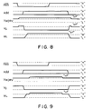
- the RAS signal When the RAS signal is set at high level (a potential corresponding to the power source Vcc, to be referred to as "H” level hereinafter), i.e., when any memory cell is not accessed, a potential VWDRV applied to the sources and back gates of the word line drive transistors 19 and 20 is kept at "H" level, i.e., the potential of the power source Vcc.
- the RAS signal goes to low level (a potential corresponding to the ground point Vss, to be referred to as "L” level) to access a memory cell, the source potential V WDRV of the word line drive transistors 19 and 20 is increased to "H + " level by capacitive coupling of the capacitor 26 arranged in the word line potential control circuit 15.
- a recognized row address Add is supplied to a row decoder, and the output from the NAND circuit 12 corresponding to the row address signal Add in the row decoder goes to "L” level. At this time, a gate potential V G of the word line drive transistor 20 goes to "L” level. Since the output from the NAND circuit 12 is set at "L” level, a MOS transistor 22 is turned off. As a result, the MOS transistor 20 is turned on, the MOS transistor 19 is turned off, and the potential of a word line WL is increased to "H + " level. Therefore, memory cells of a row connected to the word line WL in the memory cell array MCA is selected, thereby writing or reading data.
- the RAS signal is preferably input to the inverter 25 through a delay circuit (not shown) or the like.
- the source potential V WDRV of the word line drive transistors 19 and 20 is not necessarily set to be the potential of the power source Vcc.
- the source potential V WDRV is set to be equal to or lower than the potential Vcc and equal to or higher than the threshold voltage V TH2 of the transfer gate transistor 17, the potential of the word line WL can be instantaneously increased when a memory cell must be accessed.
- a word line drive transistor is constituted by a p-channel transistor, and a memory cell is constituted by an n-channel MOS transistor and an n-channel MOS capacitor.
- the word line drive transistor may be constituted by an n-channel transistor, and the memory cell may be constituted by a p-channel MOS transistor and a p-channel capacitor.
- the conductivity types of the MOS transistors are reversed, and the power source Vcc and the ground point Vss are replaced with to each other.
- the source potential of the word line drive transistor is set to be the ground potential Vss.
- the source potential V WDRV of the word line drive transistor is not necessarily set to be the ground potential Vss. Only when the source potential V WDRV is set to be equal to or higher than the potential Vss and equal to or lower than the threshold voltage of the transfer gate transistor, the potential of the word line can be instantaneously increased when a memory cell must be accessed.
- a block activation circuit 45 for selecting one block from a plurality of blocks is added to a word line potential control circuit 15 in the circuit arrangement shown in Fig. 7.
- the circuit 45 has a function of activating only a block including a memory cell to be accessed.
- the circuit 45 causes a source potential to increase to "H + " level in only a word line drive transistor included in a memory cell array to be activated.
- the block activation circuit 45 is constituted by a NAND circuit 42, p-channel MOS transistors 60, 61, 64, and 65, n-channel MOS transistors 62 and 63, and an inverter 66.
- An upper-bit row address signal Add is supplied to the NAND circuit 42.
- the NAND circuit 42 is a part of a row decoder. In Fig. 10, the NAND circuit 42 is included in the circuit 45 for descriptive convenience.
- the output terminal of the NAND circuit 42 is connected to one end of the current path of the MOS transistor 63.
- the gate of the MOS transistor 63 is connected to a power source Vcc, and the other end of the current path is connected to the drain of the MOS transistor 60 and the gates of the MOS transistors 61 and 65.
- the drain and back gate of the MOS transistor 60 are connected to the other electrode of a capacitor 26, and the gate of the MOS transistor 60 is connected to the drain of the MOS transistor 61.
- the source and back gate of the MOS transistor 61 are connected to the other electrode of the capacitor 26, and the drain of the MOS transistor 61 is connected to the drain of the MOS transistor 62 and the gate of the MOS transistor 64.
- the source of the MOS transistor 62 is connected to a ground point Vss, and the gate of the MOS transistor 62 is connected to the output terminal of the NAND circuit 42.
- the current paths of the MOS transistors 64 and 65 are connected in series between the sources of the MOS transistor 60 and 61 and the power source Vcc.
- the back gates of the MOS transistors 64 and 65 are connected to the sources and back gates of the MOS transistors 60 and 61.
- the sources and back gates of the word line drive transistors 19 and 20 are connected to a common connection point between the current paths of the MOS transistors 64 and 65.
- the input terminal of the inverter 66 is connected to the output terminal of the NAND circuit 42, and the output terminal of the inverter 66 is connected to one input terminal of a NAND circuit 12.
- the source potentials of the MOS transistors 19 and 20 are set to be V WDRV-n
- the source potentials of the MOS transistors 60 and 61 of the block activation circuit 45 are set to be V WDRV .
- the potential V WDRV is boosted to "H + " level (in this case, the recognized row address signal Add is supplied to a row decoder, and the potential V WDRV is boosted to "H + " level before the output from the NAND circuit 42 of a row designated by the row address in the row decoder goes to "H + " level).
- the MOS transistor 20 is turned on, and the MOS transistors 22 and 19 are turned off, thereby increasing the potential of a word line WL to "H + " level.
- the memory cells of the row connected to the word line WL in the selected block are selected, thereby writing and reading data.
- the row address signal Add is changed (at this time, the RAS signal is already set at "H” level, a MOS transistor 27 is OFF, the MOS transistor 28 is ON, and the MOS transistor 29 is ON), the output of the NAND circuit 12 goes to "H" level.
- the MOS transistor 20 is turned off, and the MOS transistors 22 and 19 are turned on, thereby returning the potential of the word line WL to "L" level.
- the potential V WDRV goes to "H” level by setting the RAS signal at "H” level, and the potential V WDRV-n , i.e., the source potentials of the MOS transistors 19 and 20 are returned to "H” level.
- the source potential V WDRV-n of the word line drive transistors 19 and 20 or the source potential V WDRV of the MOS transistors 60 and 61 of the block activation circuit 45 is not necessarily set to be the power source voltage Vcc.
- these source potentials are set to be equal to or lower than the potential of power source Vcc and equal to or higher than the threshold voltage V TH2 of a transfer gate transistor 17, the potential of the word line WL can be instantaneously increased when a memory cell must be accessed.
- a word line drive transistor is constituted by a p-channel MOS transistor, and a memory cell is constituted by an n-channel MOS transistor and an n-channel MOS capacitor.
- the word line drive transistor may be constituted by an n-channel MOS transistor, and the memory cell may be constituted by a p-channel MOS transistor and a p-channel MOS capacitor.
- the source potential of the word line drive transistor is set to be the ground potential Vss.
- the source potential V WDRV-n of the word line drive transistor is not necessarily set to be the ground potential Vss.
- the source potential VWDRV-n is set to be equal to or higher than the ground potential Vss and equal to or lower than the threshold voltage of the transfer gate transistor, the potential of the word line can be instantaneously increased when a memory cell must be accessed.
- n-channel MOS transistors 19', 29' and 65' can be used in place of the p-channel MOS transistors 19, 29 and 65 in the circuit shown in Fig. 10.
- D MOS transistor 29' When a D MOS transistor 29' is used, the MOS transistors 27 and 28 are not required.
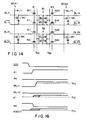
- Figs. 14 to 16 show applications of the present invention. Circuits shown in Figs. 14 and 15 are obtained by applying the present invention to a DRAM using a shared sense amplifier system.
- a memory cell array is generally divided into two parts, and a sense amplifier S/A is arranged between memory cell arrays MCAi and MCAK. That is, the current paths of switching n-channel MOS transistors 40i and 40k are connected in series between bit lines BLli and BL1k, and the current paths of switching n-channel MOS transistors 41i and 41k are connected in series between bit lines BL1i and BL1k .
- One input terminal of a sense amplifier 51 is connected to the connection point between the current paths of the MOS transistors 40i and 40k, and the other input terminal of the sense amplifier 51 is connected to the connection point between the current paths of the MOS transistors 41i and 41k.
- the current paths of switching n-channel MOS transistors 42i and 42k are connected in series between bit lines BL2i and BL2k, and the current paths of switching n-channel MOS transistors 43i and 43k are connected in series between bit lines BL2i and BL2k .
- One input terminal of a sense amplifier 52 is connected to the connection point between the current paths of the MOS transistors 42i and 42k, and the other input terminal of the sense amplifier 52 is connected to the connection point between the current paths of the MOS transistors 43i and 43k.
- Memory cells MC each having an n-channel MOS transistor and an n-channel MOS capacitor are arranged at the intersections between the bit lines BL1i, BL1k, BL1i , BL1k , BL2i, BL2k, BL2i , and BL2k and word lines WLi and WLj.
- a control signal ⁇ i is supplied to the gates of the MOS transistors 40i, 41i, 42i, and 43i, and a control signal ⁇ k is supplied to the gates of the MOS transistors 40k, 41k, 42k, and 43k.
- Fig. 15 shows a generating circuit for generating the control signals ⁇ i and ⁇ k in the circuit shown in Fig. 14.
- This circuit ON/OFF-controls the switching MOS transistors 40i, 41i, 42i, 43i, 40k, 41k, 42k, and 43k so as to selectively connect the sense amplifiers 51 and 52 to the bit lines BL1i, BL1i , BL2i, and BL2i on the memory cell array MCAi side or to the bit lines BL1k, BL1k , BL2k, and BL2k on the memory cell array MCAk side.
- Address signals Ai and Aj are supplied to the input terminals of inverters 70 and 71, respectively.
- the output terminal of the inverter 70 is connected to the input terminal of an inverter 72 and one input terminal of a NAND circuit 74.
- the output terminal of the inverter 71 is connected to the input terminal of an inverter 73 and the other input terminal of the NAND circuit 74.
- the output terminal of the inverter 72 is connected to one end of the current path of an n-channel MOS transistor 75 having a gate connected to a power source Vcc.
- the other end of the current path of the MOS transistor 75 is connected to one end of the current path of a p-channel MOS transistor 76 and the gate of a p-channel MOS transistor 77.
- One end of the current path of the MOS transistor 77 is connected to the gate of the MOS transistor 76 and one end of the current path of an n-channel MOS transistor 78.
- the other end of the current path of the MOS transistor 78 is connected to a ground point Vss, and the gate of the MOS transistor 78 is connected to the output terminal of the inverter 72.
- the other end of each of the current paths and back gates of the MOS transistors 76 and 77 are connected to a signal line 79 receiving a boost signal (a level obtained by adding a threshold voltage V TH4 of the switching MOS transistors 40i to 43i and 40k to 43k to the power source voltage Vcc) ⁇ BOOT .
- the current paths of p-channel MOS transistors 80 and 81 are directly connected between the signal line 79 and the power source Vcc.
- the back gates of the MOS transistors 80 and 81 are connected to the signal line 79.
- the gate of the MOS transistor 80 is connected to the connection point between the current paths of the MOS transistors 77 and 78.
- the current path of an n-channel MOS transistor 82 is connected between the connection point between the current paths of the MOS transistors 80 and 81 and the ground point Vss, and the gate of the MOS transistor 82 is connected to the output terminal of the inverter 73.
- the output terminal of the inverter 73 is connected to one end of the current path of an n-channel MOS transistor 83 having a gate connected to the power source Vcc.
- the other end of the current path of the MOS transistor 83 is connected to one end of the current path of a p-channel MOS transistor 84 and the gate of a p-channel MOS transistor 85.
- One end of the current path of the MOS transistor 85 is connected to the gate of the MOS transistor 84 and one end of the current path of an n-channel MOS transistor 86.
- the other end of the current path of the MOS transistor 86 is connected to the ground point Vss, and the gate of the MOS transistor 86 is connected to the output terminal of the inverter 73.
- each of the current paths and back gates of the MOS transistors 84 and 85 are connected to a signal line 87 for receiving the boost signal ⁇ BOOT .
- the current paths of p-channel MOS transistors 88 and 89 are directly connected between the signal line 87 and the power source Vcc.
- the back gates of the MOS transistors 88 and 89 are connected to the signal line 87.
- the gate of the MOS transistor 88 is connected to the connection point between the current paths of the MOS transistors 85 and 86.
- the current path of an n-channel MOS transistor 90 is connected between the connection point between the current paths of the MOS transistors 88 and 89 and the ground point Vss, and the gate of the MOS transistor 90 is connected to the output terminal of the inverter 72.
- the output terminal of the NAND circuit 74 is connected to the input terminal of an inverter 91 and the gate of an n-channel MOS transistor 92.
- the output terminal of the inverter 91 is connected to the gate of an n-channel MOS transistor 93.
- One end of the current path of the MOS transistor 92 is connected to the ground point Vss, and the other end is connected to one end of the current path of a p-channel MOS transistor 94 and the gate of a p-channel MOS transistor 95.
- One end of the current path of the MOS transistor 93 is connected to the ground point Vss, and the other end is connected to one end of the current path of the MOS transistor 95 and the gate of the MOS transistor 94.
- the boost signal ⁇ BOOT is supplied to the other ends of the current paths and back gates of the MOS transistors 94 and 95.
- the connection point between the current paths of the MOS transistors 93 and 95 is connected to the gates of the MOS transistors 81 and 89.
- the control signal ⁇ i is output from the connection point between the current paths of the MOS transistors 80 and 81, and the control signal ⁇ j is output from the connection point between the current paths of the MOS transistors 88 and 89.
- Fig. 16 is a timing chart for explaining operations of the circuits shown in Figs. 14 and 15 wherein the memory cell MC on the memory cell array MCAi is selected as an example.
- the MOS transistor 92 is turned on, and the MOS transistor 93 is turned off. Since the connection point between the current paths of the MOS transistors 93 and 95 goes to the level of the boost signal ⁇ BOOT the MOS transistor 81 is turned off.
- the address signal Aj goes to "L" level
- the output from the inverter 73 goes to "L” level
- the MOS transistor 82 is turned off.
- the control signal ⁇ i has the same potential as the boost signal ⁇ BOOT .
- the MOS transistor 85 is turned on, the MOS transistors 84 and 86 are turned off, and then the MOS transistor 88 is turned off.
- the MOS transistor 89 is turned off, since the connection point between the current paths of the MOS transistors 93 and 95 is set at the same level as that of the signal ⁇ BOOT . Since an output from the inverter 72 is set at "H” level, the MOS transistor 90 is turned off. Therefore, the control signal ⁇ k goes to "L" level.
- a potential at "Vcc + V TH4 " level and a potential at Vss level are applied to the gates of the switching MOS transistors on the selected memory cell array side and to the gates of the switching MOS transistors on the non-selected memory cell array, respectively.
- the gates of the switching MOS transistors on both the sides of the sense amplifier are at Vcc level.
- the power source voltage Vcc the voltage "Vcc + V TH4 " (V TH4 is the threshold voltage of the MOS transistors 40i to 43i and 40k to 43k), and the potential of the ground point Vss can be selectively applied to the gates of the switching MOS transistors 40i to 43i and 40k to 43k.
Landscapes
- Engineering & Computer Science (AREA)
- Microelectronics & Electronic Packaging (AREA)
- Computer Hardware Design (AREA)
- Dram (AREA)
- Semiconductor Memories (AREA)
Claims (3)
- Halbleiterspeicher mit Speicherzellen einschließlich mindestens einer Speicherzelle (10) mit einem MOS-Transistor (17) vom n-Kanal-Typ und einem MOS-Kondensator (16) vom n-Kanal-Typ sowie einem an diese Speicherzellen angeschlossenen Wortleiter (WL) mit:dadurch gekennzeichnet, daß die Wortleiter-Potentialsteuereinrichtung (15) zum Empfang eines RAS-Signals geschaltet und derart angeordnet ist, daß sie das erste Potential erzeugt, wenn das RAS-Signal inaktiv ist und das zweite Potential, wenn das RAS-Signal aktiv ist sowie dadurch, daß das erste Potential als Stromquellenpotential (VCC) eingestellt und das zweite Potential gleich dem oder größer als das Stromquellenpotential (VCC) plus der Schwellenspannung (VTH2) des MOS-Transistors (17) der Speicherzelle (10) ist.einer Wortleiter-Treibereinrichtung (11), welche einen MOS-Transistor (20) vom p-Kanal-Typ enthält, um ein Potential auf den Wortleiter zu übertragen und welche zum Ansteuern des Wortleiters (WL) betreibbar ist undeiner Wortleiter-Potentialsteuereinrichtung (15), welche derart angeordnet ist, daß sie ein erstes Potential oder ein vom ersten Potential verschiedenes zweites Potential an den MOS-Transistor (20) der Wortleiter-Treibereinrichtung (11) anzulegen vermag,
- Halbleiterspeicher mit Speicherzellen einschließlich mindestens einer Speicherzelle mit einem MOS-Transistor vom n-Kanal-Typ und einem MOS-Kondensator vom n-Kanal-Typ sowie einem an diese Speicherzellen angeschlossenen Wortleiter mit:dadurch gekennzeichnet, daß die Wortleiter-Potentialsteuereinrichtung (15) einen ersten Kondensator (33) mit einer Elektrode zum Empfang eines RAS-Signals, einen ersten MOS-Transistor (35) vom n-Kanal-Typ, dessen Strompfad zwischen der anderen Elektrode des ersten Kondensators (33) und einer ersten Stromquelle (VCC) geschaltet ist sowie mit einem an die erste Stromquelle (VCC) angeschlossenen Gate, einen Inverter (32) mit einem ersten Eingangsanschluß zum Empfang des RAS-Signals, einen zweiten Kondensator (34), dessen eine Elektrode an einen Ausgangsanschluß des Inverters (32) angeschlossen ist, einen zweiten MOS-Transistor (36) vom n-Kanal-Typ, dessen Strompfad zwischen der anderen Elektrode des zweiten Kondensators (34) und der ersten Stromquelle (VCC) geschaltet ist sowie mit einem an die andere Elektrode des ersten Kondensators angeschlossenen Gate und einen dritten MOS-Transistor (37) vom n-Kanal-Typ enthält, dessen Strompfad zwischen der anderen Elektrode des zweiten Kondensators (34) und der ersten Stromquelle (VCC) geschaltet ist sowie mit einem an die erste Stromquelle (VCC) angeschlossenen Gate, so daß das erste oder zweite Potential in Abhängigkeit vom Pegel des RAS-Signals am Verbindungspunkt zwischen dem zweiten Kondensator (34) und dem ersten und dritten MOS-Transistor (36, 37) ausgegeben wird.einer Wortleiter-Treibereinrichtung (11), welche einen MOS-Transistor (20) vom p-Kanal-Typ enthält, um ein Potential auf den Wortleiter zu übertragen und welche zum Ansteuern des Wortleiters (WL) betätigbar ist undeiner Wortleiter-Potentialsteuereinrichtung (15), welche derart angeordnet ist, daß sie ein erstes Potential oder ein vom ersten Potential verschiedenes zweites Potential an den MOS-Transistor (20) der Wortleiter-Treibereinrichtung (11) anzulegen vermag,
- Halbleiterspeicher mit Speicherzellen einschließlich mindestens einer Speicherzelle mit einem MOS-Transistor vom n-Kanal-Typ und einem MOS-Kondensator vom n-Kanal-Typ sowie einem an diese Speicherzellen angeschlossenen Wortleiter (WL) mit:einer Wortleiter-Treibereinrichtung (11), welche einen MOS-Transistor (20) vom p-Kanal-Typ enthält, um ein Potential auf den Wortleiter zu übertragen und welche zum Ansteuern des Wortleiters (WL) betätigbar ist undeiner Wortleiter-Potentialsteuereinrichtung (15), welche derart angeordnet ist, daß sie ein erstes Potential oder ein vom ersten Potential verschiedenes zweites Potential an den MOS-Transistor (20) der Wortleiter-Treibereinrichtung (11) anzulegen vermag, dadurch gekennzeichnet, daß die Wortleiter-Potentialsteuereinrichtung (15) einen Inverter (25) mit einem Eingangsanschluß zum Empfang eines RAS-Signals, einen Kondensator (26) mit einer an den Ausgangsanschluß des Inverters (25) angeschlossenen Elektrode, einen ersten Verarmungs-MOS-Transistor (29') vom n-Kanal-Typ, dessen eines Ende des Strompfades an die andere Elektrode des Kondensators (33) und dessen anderes Ende des Strompfades an eine erste Stromquelle (VCC) angeschlossen ist sowie mit einem Gate zum Empfang des RAS-Signals, einen zweiten MOS-Transistor (63) vom n-Kanal-Typ, mit einem Ende des Strompfades zum Empfang eines Ausgangssignals eines Block-Decoders (42) sowie mit einem an die erste Stromquelle (VCC) angeschlossenen Gate, einen dritten MOS-Transistor (60) vom p-Kanal-Typ, dessen eines Ende des Strompfades an das andere Ende des Strompfades des zweiten MOS-Transistors (63) und dessen anderes Ende des Strompfades und dessen hinteres Gate an die andere Elektrode des zweiten Kondensators (26) angeschlossen sind, einen vierten MOS-Transistor (61) vom p-Kanal-Typ, dessen eines Ende des Strompfades an ein Gate des dritten MOS-Transistors (60), dessen anderes Ende des Strompfades und dessen hinteres Gate an die andere Elektrode des zweiten Kondensators (26) und dessen Gate an das eine Ende des Strompfades des dritten MOS-Transistors (60) angeschlossen sind, einen fünften MOS-Transistor (62) vom n-Kanal-Typ, dessen eines Ende des Strompfades an das eine Ende des Strompfades des vierten MOS-Transistors (61), dessen anderes Ende des Strompfades an eine zweite Stromquelle (VSS) sowie dessen Gate zum Empfang eines Ausgangssignals von einem Block-Decoder (42) angeschlossen sind, einen sechsten MOS-Transistor (64) vom p-Kanal-Typ, dessen eines Ende des Strompfades sowie hinteres Gate an die andere Elektrode des Kondensators (26), dessen anderes Ende des Strompfades an die Wortleiter-Treibereinrichtung (11) sowie dessen Gate an einen Verbindungspunkt zwischen den Strompfaden des vierten und des fünften MOS-Transistors (61, 62) angeschlossen sind, einen siebenten Verarmungs-MOS-Transistor (65') vom p-Kanal-Typ, dessen eines Ende des Strompfades an das andere Ende des Strompfades des sechsten MOS-Transistors (64), dessen anderes Ende des Strompfades an die erste Stromquelle (VCC) sowie dessen Gate an einen Verbindungspunkt zwischen den Strompfaden des vierten und des fünften MOS-Transistors (61, 62) und dessen hinteres Gate an die andere Elektrode des Kondensators (26) angeschlossen sind und einen Inverter (66) mit einem Eingangsanschluß zum Empfang des Ausgangssignals vom Block-Decoder (42) enthält, wobei der Inverter (66) ein Ausgangssignal einem Eingangsanschluß eines Zeilen-Decoders (12) zuführt und am Verbindungspunkt zwischen dem sechsten und dem siebenten MOS-Transistor (64, 65') in Abhängigkeit vom Pegel des RAS-Signals das erste oder das zweite Potential ausgegeben wird.
Applications Claiming Priority (2)
| Application Number | Priority Date | Filing Date | Title |
|---|---|---|---|
| JP2239893A JPH07111826B2 (ja) | 1990-09-12 | 1990-09-12 | 半導体記憶装置 |
| JP239893/90 | 1990-09-12 |
Publications (3)
| Publication Number | Publication Date |
|---|---|
| EP0475407A2 EP0475407A2 (de) | 1992-03-18 |
| EP0475407A3 EP0475407A3 (en) | 1993-03-17 |
| EP0475407B1 true EP0475407B1 (de) | 1998-03-25 |
Family
ID=17051430
Family Applications (1)
| Application Number | Title | Priority Date | Filing Date |
|---|---|---|---|
| EP91115475A Expired - Lifetime EP0475407B1 (de) | 1990-09-12 | 1991-09-12 | DRAM mit einem Wortleitungsbetriebsschaltungssystem |
Country Status (5)
| Country | Link |
|---|---|
| US (3) | US5335205A (de) |
| EP (1) | EP0475407B1 (de) |
| JP (1) | JPH07111826B2 (de) |
| KR (1) | KR950010621B1 (de) |
| DE (1) | DE69129138T2 (de) |
Families Citing this family (32)
| Publication number | Priority date | Publication date | Assignee | Title |
|---|---|---|---|---|
| JPH04225182A (ja) | 1990-12-26 | 1992-08-14 | Toshiba Corp | 半導体記憶装置 |
| US5255224A (en) * | 1991-12-18 | 1993-10-19 | International Business Machines Corporation | Boosted drive system for master/local word line memory architecture |
| US5668485A (en) * | 1992-05-21 | 1997-09-16 | Texas Instruments Incorporated | Row decoder with level translator |
| US5452251A (en) | 1992-12-03 | 1995-09-19 | Fujitsu Limited | Semiconductor memory device for selecting and deselecting blocks of word lines |
| JP2967021B2 (ja) * | 1993-01-25 | 1999-10-25 | 株式会社東芝 | 半導体メモリ装置 |
| US5406140A (en) * | 1993-06-07 | 1995-04-11 | National Semiconductor Corporation | Voltage translation and overvoltage protection |
| JP3562725B2 (ja) * | 1993-12-24 | 2004-09-08 | 川崎マイクロエレクトロニクス株式会社 | 出力バッファ回路、および入出力バッファ回路 |
| JP3090833B2 (ja) * | 1993-12-28 | 2000-09-25 | 株式会社東芝 | 半導体記憶装置 |
| JP3337564B2 (ja) * | 1994-09-16 | 2002-10-21 | 松下電器産業株式会社 | 半導体記憶装置 |
| JPH08235877A (ja) * | 1995-02-24 | 1996-09-13 | Toshiba Corp | 不揮発性半導体メモリ装置 |
| JP2720812B2 (ja) * | 1995-03-17 | 1998-03-04 | 日本電気株式会社 | 半導体記憶装置 |
| JPH08274612A (ja) * | 1995-03-31 | 1996-10-18 | Nec Corp | 半導体装置 |
| JP3497601B2 (ja) * | 1995-04-17 | 2004-02-16 | 松下電器産業株式会社 | 半導体集積回路 |
| KR0179553B1 (ko) * | 1995-12-29 | 1999-04-15 | 김주용 | 로오 디코더 및 컬럼 디코더 회로 |
| US5703827A (en) * | 1996-02-29 | 1997-12-30 | Monolithic System Technology, Inc. | Method and structure for generating a boosted word line voltage and a back bias voltage for a memory array |
| US5760608A (en) * | 1996-10-21 | 1998-06-02 | Hewlett-Packard Co. | High speed, low clock load register dump circuit |
| US5777940A (en) * | 1996-11-12 | 1998-07-07 | Winbond Electronics Corp. | Circuit with regulated power supply for reducing memory device operating power |
| US5835438A (en) * | 1996-12-24 | 1998-11-10 | Mosaid Technologies Incorporated | Precharge-enable self boosting word line driver for an embedded DRAM |
| JPH10241364A (ja) * | 1997-02-28 | 1998-09-11 | Toshiba Corp | Dram装置及びロジック混載lsi |
| DE19739807C2 (de) * | 1997-09-10 | 2000-06-15 | Siemens Ag | Pegelumsetzschaltung |
| US6215708B1 (en) * | 1998-09-30 | 2001-04-10 | Integrated Device Technology, Inc. | Charge pump for improving memory cell low VCC performance without increasing gate oxide thickness |
| US7221605B2 (en) * | 2004-08-31 | 2007-05-22 | Micron Technology, Inc. | Switched capacitor DRAM sense amplifier with immunity to mismatch and offsets |
| US7176719B2 (en) * | 2004-08-31 | 2007-02-13 | Micron Technology, Inc. | Capacitively-coupled level restore circuits for low voltage swing logic circuits |
| KR101020280B1 (ko) * | 2008-04-22 | 2011-03-07 | 주식회사 하이닉스반도체 | 레벨시프터 |
| JP2011044186A (ja) * | 2009-08-19 | 2011-03-03 | Oki Semiconductor Co Ltd | ワード線駆動装置 |
| US8537593B2 (en) | 2011-04-28 | 2013-09-17 | Sandisk Technologies Inc. | Variable resistance switch suitable for supplying high voltage to drive load |
| US8395434B1 (en) * | 2011-10-05 | 2013-03-12 | Sandisk Technologies Inc. | Level shifter with negative voltage capability |
| JP6125850B2 (ja) * | 2012-02-09 | 2017-05-10 | 株式会社半導体エネルギー研究所 | 半導体装置及び半導体装置の作製方法 |
| JP6333028B2 (ja) * | 2013-04-19 | 2018-05-30 | 株式会社半導体エネルギー研究所 | 記憶装置及び半導体装置 |
| US9330776B2 (en) | 2014-08-14 | 2016-05-03 | Sandisk Technologies Inc. | High voltage step down regulator with breakdown protection |
| TWI686806B (zh) * | 2019-02-13 | 2020-03-01 | 旺宏電子股份有限公司 | 記憶體裝置 |
| US11114148B1 (en) * | 2020-04-16 | 2021-09-07 | Wuxi Petabyte Technologies Co., Ltd. | Efficient ferroelectric random-access memory wordline driver, decoder, and related circuits |
Family Cites Families (15)
| Publication number | Priority date | Publication date | Assignee | Title |
|---|---|---|---|---|
| JPS5271141A (en) * | 1975-12-10 | 1977-06-14 | Hitachi Ltd | Word line driving circuit |
| JPS5862895A (ja) * | 1981-10-12 | 1983-04-14 | Mitsubishi Electric Corp | 半導体記憶回路 |
| JPS58185091A (ja) * | 1982-04-24 | 1983-10-28 | Toshiba Corp | 昇圧電圧出力回路および昇圧電圧出力回路を備えたアドレスデコ−ド回路 |
| JPS58188388A (ja) * | 1982-04-28 | 1983-11-02 | Toshiba Corp | 半導体記憶装置 |
| JPS61144790A (ja) * | 1984-12-18 | 1986-07-02 | Sharp Corp | アドレスデコ−ダ回路 |
| JPS61151898A (ja) * | 1984-12-26 | 1986-07-10 | Fujitsu Ltd | 半導体記憶装置におけるワ−ド線ドライバ回路 |
| JPS6238592A (ja) * | 1985-08-14 | 1987-02-19 | Fujitsu Ltd | 相補型メモリの行選択線駆動回路 |
| US4769792A (en) * | 1986-10-28 | 1988-09-06 | Kabushiki Kaisha Toshiba | Semiconductor memory device with voltage bootstrap |
| JPH0632230B2 (ja) * | 1987-03-31 | 1994-04-27 | 株式会社東芝 | 半導体不揮発性記憶装置 |
| US4820941A (en) * | 1988-02-01 | 1989-04-11 | Texas Instruments Incorporated | Decoder driver circuit for programming high-capacitance lines |
| JPH01317022A (ja) * | 1988-06-16 | 1989-12-21 | Toshiba Corp | 電源切り換え回路 |
| JPH0793022B2 (ja) * | 1988-12-24 | 1995-10-09 | 株式会社東芝 | 半導体メモリ集積回路 |
| JPH02247892A (ja) * | 1989-03-20 | 1990-10-03 | Fujitsu Ltd | ダイナミックランダムアクセスメモリ |
| JPH0438790A (ja) * | 1990-06-01 | 1992-02-07 | Toshiba Corp | ダイナミック型半導体記憶装置 |
| US5136190A (en) * | 1991-08-07 | 1992-08-04 | Micron Technology, Inc. | CMOS voltage level translator circuit |
-
1990
- 1990-09-12 JP JP2239893A patent/JPH07111826B2/ja not_active Expired - Fee Related
-
1991
- 1991-09-09 KR KR1019910015687A patent/KR950010621B1/ko not_active Expired - Fee Related
- 1991-09-11 US US07/757,632 patent/US5335205A/en not_active Expired - Lifetime
- 1991-09-12 DE DE69129138T patent/DE69129138T2/de not_active Expired - Fee Related
- 1991-09-12 EP EP91115475A patent/EP0475407B1/de not_active Expired - Lifetime
-
1994
- 1994-05-10 US US08/240,368 patent/US5550504A/en not_active Expired - Lifetime
-
1996
- 1996-06-05 US US08/658,572 patent/US5619162A/en not_active Expired - Lifetime
Also Published As
| Publication number | Publication date |
|---|---|
| JPH04121894A (ja) | 1992-04-22 |
| JPH07111826B2 (ja) | 1995-11-29 |
| EP0475407A3 (en) | 1993-03-17 |
| US5550504A (en) | 1996-08-27 |
| EP0475407A2 (de) | 1992-03-18 |
| KR950010621B1 (ko) | 1995-09-20 |
| DE69129138T2 (de) | 1998-08-20 |
| US5335205A (en) | 1994-08-02 |
| KR930006728A (ko) | 1993-04-21 |
| DE69129138D1 (de) | 1998-04-30 |
| US5619162A (en) | 1997-04-08 |
Similar Documents
| Publication | Publication Date | Title |
|---|---|---|
| EP0475407B1 (de) | DRAM mit einem Wortleitungsbetriebsschaltungssystem | |
| US5566120A (en) | Apparatus and method for controlling transistor current leakage | |
| US5859799A (en) | Semiconductor memory device including internal power supply circuit generating a plurality of internal power supply voltages at different levels | |
| KR0183413B1 (ko) | 차지-펌프형 부스터 회로 | |
| US5652730A (en) | Semiconductor memory device having hierarchical boosted power-line scheme | |
| EP0173980A2 (de) | Integrierte Halbleiterschaltungsanordnung | |
| KR19980033971A (ko) | 반도체 집적 회로 장치 | |
| US5132575A (en) | Method for providing multi-level potentials at a sense node | |
| US5792682A (en) | Method for reducing charge loss | |
| US4578781A (en) | MIS transistor circuit | |
| US4110841A (en) | Level shifter and sense-refresh detector | |
| US6288952B1 (en) | System for improved memory cell access | |
| US5677889A (en) | Static type semiconductor device operable at a low voltage with small power consumption | |
| US5777934A (en) | Semiconductor memory device with variable plate voltage generator | |
| US5376837A (en) | Semiconductor integrated circuit device having built-in voltage drop circuit | |
| US5166554A (en) | Boot-strapped decoder circuit | |
| JPS6052997A (ja) | 半導体記憶装置 | |
| US6430091B2 (en) | Semiconductor memory device having reduced current consumption at internal boosted potential | |
| EP0318094B1 (de) | Integrierte Speicherschaltung mit innerer Speisespannungsregelung | |
| US20260080935A1 (en) | Memory device | |
| JP2851786B2 (ja) | 半導体メモリ | |
| US5578942A (en) | Super VCC detection circuit | |
| KR0170694B1 (ko) | 반도체 메모리 장치의 센스 증폭기 풀다운 구동회로 | |
| JP2986939B2 (ja) | ダイナミックram | |
| KR950009235B1 (ko) | 반도체 메모리 장치의 워드라인 구동회로 |
Legal Events
| Date | Code | Title | Description |
|---|---|---|---|
| PUAI | Public reference made under article 153(3) epc to a published international application that has entered the european phase |
Free format text: ORIGINAL CODE: 0009012 |
|
| 17P | Request for examination filed |
Effective date: 19910912 |
|
| AK | Designated contracting states |
Kind code of ref document: A2 Designated state(s): DE FR GB |
|
| PUAL | Search report despatched |
Free format text: ORIGINAL CODE: 0009013 |
|
| AK | Designated contracting states |
Kind code of ref document: A3 Designated state(s): DE FR GB |
|
| 17Q | First examination report despatched |
Effective date: 19951222 |
|
| GRAG | Despatch of communication of intention to grant |
Free format text: ORIGINAL CODE: EPIDOS AGRA |
|
| GRAG | Despatch of communication of intention to grant |
Free format text: ORIGINAL CODE: EPIDOS AGRA |
|
| GRAH | Despatch of communication of intention to grant a patent |
Free format text: ORIGINAL CODE: EPIDOS IGRA |
|
| GRAH | Despatch of communication of intention to grant a patent |
Free format text: ORIGINAL CODE: EPIDOS IGRA |
|
| GRAA | (expected) grant |
Free format text: ORIGINAL CODE: 0009210 |
|
| AK | Designated contracting states |
Kind code of ref document: B1 Designated state(s): DE FR GB |
|
| REF | Corresponds to: |
Ref document number: 69129138 Country of ref document: DE Date of ref document: 19980430 |
|
| ET | Fr: translation filed | ||
| PLBE | No opposition filed within time limit |
Free format text: ORIGINAL CODE: 0009261 |
|
| STAA | Information on the status of an ep patent application or granted ep patent |
Free format text: STATUS: NO OPPOSITION FILED WITHIN TIME LIMIT |
|
| 26N | No opposition filed | ||
| REG | Reference to a national code |
Ref country code: GB Ref legal event code: IF02 |
|
| PGFP | Annual fee paid to national office [announced via postgrant information from national office to epo] |
Ref country code: FR Payment date: 20080915 Year of fee payment: 18 |
|
| PGFP | Annual fee paid to national office [announced via postgrant information from national office to epo] |
Ref country code: GB Payment date: 20080917 Year of fee payment: 18 |
|
| PGFP | Annual fee paid to national office [announced via postgrant information from national office to epo] |
Ref country code: DE Payment date: 20080926 Year of fee payment: 18 |
|
| GBPC | Gb: european patent ceased through non-payment of renewal fee |
Effective date: 20090912 |
|
| REG | Reference to a national code |
Ref country code: FR Ref legal event code: ST Effective date: 20100531 |
|
| PG25 | Lapsed in a contracting state [announced via postgrant information from national office to epo] |
Ref country code: DE Free format text: LAPSE BECAUSE OF NON-PAYMENT OF DUE FEES Effective date: 20100401 Ref country code: FR Free format text: LAPSE BECAUSE OF NON-PAYMENT OF DUE FEES Effective date: 20090930 |
|
| PG25 | Lapsed in a contracting state [announced via postgrant information from national office to epo] |
Ref country code: GB Free format text: LAPSE BECAUSE OF NON-PAYMENT OF DUE FEES Effective date: 20090912 |