EP0928062B1 - Verfahren und Schaltung zur Korrektur der Linearität für Leistungsverstärker und Verstärker mit einer solchen Schaltung - Google Patents
Verfahren und Schaltung zur Korrektur der Linearität für Leistungsverstärker und Verstärker mit einer solchen Schaltung Download PDFInfo
- Publication number
- EP0928062B1 EP0928062B1 EP98403337A EP98403337A EP0928062B1 EP 0928062 B1 EP0928062 B1 EP 0928062B1 EP 98403337 A EP98403337 A EP 98403337A EP 98403337 A EP98403337 A EP 98403337A EP 0928062 B1 EP0928062 B1 EP 0928062B1
- Authority
- EP
- European Patent Office
- Prior art keywords
- signal
- amplified
- circuit
- components
- modulation
- Prior art date
- Legal status (The legal status is an assumption and is not a legal conclusion. Google has not performed a legal analysis and makes no representation as to the accuracy of the status listed.)
- Expired - Lifetime
Links
- 238000012937 correction Methods 0.000 title claims description 19
- 238000000034 method Methods 0.000 title claims description 5
- 230000006870 function Effects 0.000 claims description 10
- 238000001514 detection method Methods 0.000 claims description 7
- 230000003321 amplification Effects 0.000 claims description 6
- 238000003199 nucleic acid amplification method Methods 0.000 claims description 6
- 238000006243 chemical reaction Methods 0.000 claims description 4
- 230000010363 phase shift Effects 0.000 claims description 4
- 238000012986 modification Methods 0.000 claims description 2
- 230000004048 modification Effects 0.000 claims description 2
- 238000004364 calculation method Methods 0.000 description 8
- 238000010586 diagram Methods 0.000 description 5
- 238000010606 normalization Methods 0.000 description 5
- 230000017105 transposition Effects 0.000 description 4
- 240000008042 Zea mays Species 0.000 description 3
- 238000012546 transfer Methods 0.000 description 3
- 230000003044 adaptive effect Effects 0.000 description 2
- 230000007547 defect Effects 0.000 description 2
- 238000001914 filtration Methods 0.000 description 2
- 239000000523 sample Substances 0.000 description 2
- 238000001228 spectrum Methods 0.000 description 2
- 241000238876 Acari Species 0.000 description 1
- 241001080024 Telles Species 0.000 description 1
- 230000000712 assembly Effects 0.000 description 1
- 238000000429 assembly Methods 0.000 description 1
- 230000002238 attenuated effect Effects 0.000 description 1
- 230000000295 complement effect Effects 0.000 description 1
- 238000001816 cooling Methods 0.000 description 1
- 238000013500 data storage Methods 0.000 description 1
- 230000000694 effects Effects 0.000 description 1
- 235000021183 entrée Nutrition 0.000 description 1
- 238000013213 extrapolation Methods 0.000 description 1
- 238000009499 grossing Methods 0.000 description 1
- 230000003071 parasitic effect Effects 0.000 description 1
- 238000012545 processing Methods 0.000 description 1
- 230000000717 retained effect Effects 0.000 description 1
- 230000000630 rising effect Effects 0.000 description 1
- 238000005070 sampling Methods 0.000 description 1
- 230000003595 spectral effect Effects 0.000 description 1
Images

Classifications
-
- H—ELECTRICITY
- H03—ELECTRONIC CIRCUITRY
- H03F—AMPLIFIERS
- H03F1/00—Details of amplifiers with only discharge tubes, only semiconductor devices or only unspecified devices as amplifying elements
- H03F1/32—Modifications of amplifiers to reduce non-linear distortion
- H03F1/3241—Modifications of amplifiers to reduce non-linear distortion using predistortion circuits
- H03F1/3294—Acting on the real and imaginary components of the input signal
-
- H—ELECTRICITY
- H03—ELECTRONIC CIRCUITRY
- H03F—AMPLIFIERS
- H03F1/00—Details of amplifiers with only discharge tubes, only semiconductor devices or only unspecified devices as amplifying elements
- H03F1/32—Modifications of amplifiers to reduce non-linear distortion
- H03F1/3241—Modifications of amplifiers to reduce non-linear distortion using predistortion circuits
- H03F1/3247—Modifications of amplifiers to reduce non-linear distortion using predistortion circuits using feedback acting on predistortion circuits
-
- H—ELECTRICITY
- H03—ELECTRONIC CIRCUITRY
- H03F—AMPLIFIERS
- H03F2201/00—Indexing scheme relating to details of amplifiers with only discharge tubes, only semiconductor devices or only unspecified devices as amplifying elements covered by H03F1/00
- H03F2201/32—Indexing scheme relating to modifications of amplifiers to reduce non-linear distortion
- H03F2201/3233—Adaptive predistortion using lookup table, e.g. memory, RAM, ROM, LUT, to generate the predistortion
Definitions
- the present invention relates to linearity correction of power amplifiers and, in particular, amplifiers of power used in radio frequencies.
- EP 0 731 556 It is also known from EP 0 731 556 to perform an adaptive pre-distortion of the modulated signal using tables addressed as a function of the modulating signal and updated from a comparison between the modulation signals before the pre-distortion. and after the amplification.
- the object of the present invention is to avoid or, at least reduce the disadvantages of the correctors discussed above. This is achieved by adaptively pre-distorting the modulated signal using tables addressed according to the modulating signal and updated from a comparison between the modulation signals before the pre-distortion and after amplification, which are transposed into baseband before said comparison.
- a method for correcting linearity for power amplifier in which a pre-distortion is performed, on a modulated signal to be amplified, from coefficients memorized, this method of controlling the supply of coefficients according to the modulation of the signal to be amplified, to be transposed in baseband the signals to be amplified and amplified and to be modified possibly the memorized coefficients according to a comparison between the two signals resulting from the transposition, characterized in that the signal to be amplified and the signals transposed into baseband are each divided into two orthogonal components I and Q, in that the pre-distortion is performed separately on each component orthogonal signals I and Q of the signal to be amplified, based on the reports from the components I of the transposed signals from the signal to be amplified and the amplified signal and secondly Q components of these same signals transposed and that the two components obtained after pre-distortion are combined to form the input signal of the amplifier.
- a linearity corrector for power amplifier, comprising a modulation circuit for receive a modulated signal to amplify and pre-distort before amplification by the power amplifier and a memory circuit to control the modulation effected by the modulation circuit, characterized in that has a detection circuit for, depending on the modulation of the signal to amplify, provide a memory circuit address, a first and a second baseband transposer to receive respectively the signals to amplify and amplified, and a processor to receive the address and to compare the signals provided by the transposers in order to calculate modifications to be made to the contents of the memory circuit.
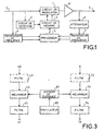
- FIG. 1 represents a power RF amplifier, A, equipped with a linearity corrector, 1 to 7.
- the assembly according to Figure 1 is for linearly amplifying an analog input signal, E, consisting of by an RF carrier modulated by an information signal; mounting provides an output signal noted S in the figure.
- the signal E is applied to the input of the carrier signal of a modulation circuit 1, at the input of a detection circuit 2 and at the input of a frequency transposer 4.
- a memory circuit 3 the content of which is addressed by the signal output of the detection circuit 2, provides the circuit 1, on two channels in quadrature I, Q, a modulation for signal E.
- the output signal S is applied via an attenuator 6 to the input of a frequency transposer 7.
- the outputs, in quadrature, I and Q, frequency transposers 4 and 7 are connected to a processor 5 which controls the contents of the circuit of memory 3.
- FIG. 2 is a more detailed view of the assembly according to FIG. 1.
- a 90 ° differential phase shifter, 20, receives the signal E and delivers on its two outputs signals I and Q with equal power but in phase quadrature; these signals are applied respectively to the first inputs of two analog multipliers 11, 12 and the outputs of the multipliers are respectively connected to the inputs of a linear adder, 13, of two-way combiner type whose output is connected to the input of a amplifier A.
- the circuits 10 to 13 correspond to the modulation circuit 1 of FIG. 1 while the amplifier A constitutes the power amplifier bearing the same reference in FIG. 1.
- the multipliers 11, 12 are AD 834 type multipliers of ANALOG DEVICES.
- An analog-digital converter 20 receives the signal E.
- This converter of the AD 9042 type of ANALOG DEVICES, has its output connected to the input of an absolute value passing circuit 21; circuit 21 performs an exclusive OR.
- the converter having a format of output of the type "complement to 2", it is sufficient to perform an exclusive OR between the sign bit and the other bits to obtain the absolute value.
- a low-pass filter made in digital cable form, 22, also called FIR according to the acronym of its Anglo-Saxon name, finite impulse responce, receives the output signal of the circuit 21; this HARRIS HSP 43168 type filter provides on its output a filtered digital signal representative of the amplitude value at time t of the envelope of signal E; this digital signal is applied to an input of a processor 5 and, through a switching circuit 23, controlled by the processor 5, to the addressing input of a digital memory 30 which has two separate cells at each of his addresses.
- the circuits 20 to 23 correspond to the detection circuit 2 of FIG. 1 while the processor 5 constitutes the processor bearing the same reference in FIG.
- the input signal is reconstructed by adding the signals of output of the phase shifter in an amplifier MAXIM 408 of MAXIM MAX. This solution is adopted to leave, out of the loop, the phase error absolute as a function of the frequency of the phase-shifter 10 and keep only its differential phase shift, which remains constant.
- An analog-digital converter, 41, of the AD 9042 type of ANALOG DEVICES, has its input connected to the output of the adder 40 and its output connected to the input of a frequency converter 42 of the HSP type 50016 of HARRIS; this converter 42 is a band converter of base I and Q whose two output channels are connected to the processor 5.
- Part of the output signal S of amplifier A is applied, via an attenuator, 6, constituted by a probe, at the input of a converter analog-digital 70 whose output is connected to the input of a frequency converter 71.
- the circuits 70, 71 are respectively identical to the circuits 41, 42 and the two output channels of the converter 71 are connected to the processor 5.
- the memory 30 whose content is provided by the processor 5 and whose addressing is done by the circuit 23, provides on two paths, I and Q, correction coefficients to pre-distort the signal at amplify. These paths are respectively connected to the inputs of two digital-analog converters 31, 32, of type AD 7945 of ANALOG DEVICES. The outputs of the converters 31, 32 are respectively connected to the inputs of two low-pass analog filters 33, 34 and the outputs of these filters are respectively connected to seconds inputs of the multipliers 11, 12.
- the two analog-to-digital converters 41, 70 and the two frequency converters 42, 71 operate with the same synchronism and, in addition, both frequency converters have exactly the same configuration.
- the transit times of the signals in the circuits 41, 42 and in the circuits 70, 71 are therefore equal.
- the frequency converters keep the phase information, that is, a phase rotation of n degrees at the input is n degrees to the output, regardless of the frequency, and that they retain the information amplitude. So the outputs of the converters are the faithful replicas of their entries.
- the determination of the correction coefficients to be introduced in the memory 30 can be performed in different ways; hereinafter it is indicated how it is performed in the example embodiment that served to the present description.
- the data available to processor 5 is presented under the form of numerical values obtained from samplings performed in analog-to-digital converters 20, 41, 70; he This is the amplitude of the input signal, input I and Q, I and Q of exit.
- the coefficients introduced into the memory 30 are, everywhere, unit coefficients; the multiplicative factor applied to the second input of the multipliers 11 and 12 is then 1 and the signal entry does not undergo any correction.
- the acquisition is performed to contain two explorations the amplitude scale, one rising and the other descending; this is obtained by modulating the input signal by a sawtooth symmetrical.
- Five simultaneous acquisitions are thus made: on the I and Q signals of the converters 42 and 71 and on the amplitude signal provided by the filter 22. Then is carried out a normalization in peak amplitude and in the middle phase of the output signals with the input signals; this standardization will be specified later.
- the ratios of the ratio ls / ls and Qe / Qs are calculated and stored at the same address but in separate boxes of a table temporary internal memory of the processor 5; the storage address is given by the amplitude sample that is to say by the output signal of the filter 22; the address has two separate boxes, one for the / Is, the other for Qe / Qs. Because, on the one hand, the number of samples is much higher important as the number of addresses, and that, on the other hand, some samples are eliminated, each address can inherit a number of calculations between zero and "number of samples / number of addresses".
- the provisional table contains, at some addresses, the sum of one to "number of samples / number Ie / Is and Qe / Qs ratio pairs are averaged. Other addresses do not contain any value; values calculated by Linear interpolations are introduced. As for both ends of the table, the values to be entered are calculated by extrapolation.
- Amplitude normalization consists simply of calculating the maximum modules, ie the square root of I 2 + Q 2 , for the, Qe and Is, Qs, to report and multiply all Is, Qs by this report.
- the modulation circuit 1 is only used in one quadrant.
- the dynamic phase error of the amplifier, A hardly exceeding ⁇ 15 °, a single quadrant is largely sufficient since it allows theoretically to make up ⁇ 45 °.
- the other point of view is that we must reset the output signal in the middle phase with the signal input.
- the solution adopted in the example described was to number the samples changing sign in the signals le, and Is, to determine the average difference in number of clock ticks and then shift all Is signals, Qs of the value of this gap to make them coincide with the, Qe.
- the correction coefficients obtained by normalization and calculation, and stored in a temporary table in the internal memory of the processor 5, are multiplied by the transfer function of the modulation circuit 1.
- the results obtained are transferred to the memory 30, where it can be provided a smoothing operation by calculating a sliding average in a window of adjustable width; this classic operation performs a low-pass filtering of first order that has the property of having a cutoff frequency proportional to the frequency of the addressing signal that is to say of the envelope.
- the calculation operation of the correction coefficients can then be repeated, but this time no longer starting from unit coefficients in the memory 30 but coefficients already contained in this memory and the new coefficients are obtained by multiplying the old ones by the corresponding values in the provisional table.
- the variation of the gain of the amplification chain being a function very slow in time, does not require significant resources from processor 5 to perform a "refresh" of the coefficients of correction with the amplified signal during normal operation, that is to say using any signal and not a specific signal such as chosen for the acquisition discussed above.
- the present invention is not limited to the example described. It is as well as the determination of the module of the input signal E, carried out by the circuits 20, 21, 22 according to FIG. 2, can be carried out with a detector Analog followed by a low-pass filter and an analog-to-digital converter.
- the determination of the input module can even be made by calculating the square root of I 2 + Q 2 , where I and Q are the signals of the two output channels of the converter 42; in this case the circuits 20 to 23 no longer exist but there is need for a fast processing by the computing unit and a small delay in the converter 42.
- Frequency conversions made by the converters 42 and 70 can also be obtained by calculation using a memory for the calculation program and data storage.
- Figure 3 shows a possibility of transposition under these conditions.
- the circuits of FIG. 3 are to be inserted between the circuits 40, 41 on the one hand and 6, 70 on the other hand.
- the output of the adder 40 is coupled, possibly by a filter 43, at the RF input of a mixer 44 whose IF output is coupled by a low-pass filter 45 at the input of the analog-to-digital converter 41.
- the output of the attenuator 6 is coupled, possibly by a filter 72, to the RF input of a mixer 73 whose IF output is coupled by a low-pass filter 74 to the input of the analog-digital converter 70.
- the abbreviations RF, FI and OL used in this document respectively mean radio frequency, intermediate frequency and local oscillator.
- a fixed frequency oscillator 80 driven by the same frequency than the rest of the assembly, delivers a signal that is applied, via a power divider 81 at the inputs OL of the mixers 44 and 73.
- filters 43, 72 depends on the relationship between on the one hand the frequency band covered at the input of the sampler of the analog-digital converter and on the other hand that covered by the amplifier to be linearized; this is called filtering folds of spectra.
Landscapes
- Physics & Mathematics (AREA)
- Nonlinear Science (AREA)
- Engineering & Computer Science (AREA)
- Power Engineering (AREA)
- Amplifiers (AREA)
- Digital Transmission Methods That Use Modulated Carrier Waves (AREA)
Claims (6)
- Verfahren zur Linearitätskorrektur für einen Leistungsverstärker, bei dem eine Vorverzerrung eines zu verstärkenden modulierten Signals (E) aufgrund von gespeicherten Koeffizienten durchgeführt wird, wobei dieses Verfahren darin besteht, die Lieferung der Koeffizienten in Abhängigkeit von der Modulation des zu verstärkenden Signals zu steuern, das zu verstärkende (E) und das verstärkte Signal (S) in das Basisband umzusetzen und ggf. die gespeicherten Koeffizienten in Abhängigkeit von einem Vergleich zwischen den beiden aus der Umsetzung stammenden Signalen zu verändern, dadurch gekennzeichnet, dass das zu verstärkende Signal und die in das Basisband umgesetzten Signale je in zwei orthogonale Komponenten I und Q aufgeteilt sind, dass die Vorverzerrung getrennt an jeder der orthogonalen Komponenten I und Q des zu verstärkenden Signals ausgehend von den Verhältnissen einerseits der Komponenten I der umgesetzten Signale, die von dem zu verstärkenden Signal und von dem verstärkten Signal kommen, und andererseits der Komponenten Q dieser gleichen umgesetzten Signale durchgeführt wird, und dass die beiden nach der Vorverzerrung erhaltenen Komponenten kombiniert werden, um das Eingangssignal des Verstärkers (A) zu bilden.
- Linearitätskorrekturorgan für einen Leistungsverstärker, mit einer Modulationsschaltung (1), die ein zu verstärkendes moduliertes Signal (E) empfangen und es vor der Verstärkung durch den Leistungsverstärker (A) vorverzerren soll, und mit einer Speicherschaltung (3), um die durch die Modulationsschaltung durchgeführte Modulation zu steuern, dadurch gekennzeichnet, dass es eine Erfassungsschaltung (2), die in Abhängigkeit von der Modulation des zu verstärkenden Signals eine Adresse der Speicherschaltung liefert, einen ersten (4) und einen zweiten Umsetzer (7) in das Basisband, die das zu verstärkende (E) bzw. das verstärkte Signal (S) empfangen, und einen Prozessor (5) aufweist, der die Adresse empfängt und die von den Umsetzern gelieferten Signale vergleicht, um ggf. am Inhalt der Speicherschaltung durchzuführende Veränderungen zu berechnen.
- Linearitätskorrekturorgan nach Anspruch 2, dadurch gekennzeichnet, dass die Speicherschaltung (30) eine eindimensionale Tabelle bildet, und dass die Erfassungsschaltung (2) dazu bestimmt ist, die Adresse ausgehend vom Modul des Modulationssignals zu liefern.
- Linearitätskorrekturorgan nach Anspruch 2, dadurch gekennzeichnet, dass die Modulationsschaltung (1) Phasenverschiebungsmittel (10), die das zu verstärkende Signal in zwei orthogonale Komponenten I und Q aufteilen, ein erstes und ein zweites Multiplizierorgan (11, 12), die an je einem ersten Eingang eine der beiden Komponenten empfangen, und ein Ausgangsaddierglied (13) mit zwei Eingängen, die mit den beiden Multiplizierorganen (11, 12) gekoppelt sind, und mit einem Ausgang aufweist, der mit dem Verstärker (A) gekoppelt ist, dass jeder Umsetzer (40, 41, 42; 6, 70, 71) sein Signal digital in Form von zwei Komponenten I und Q in Quadratur liefert, dass die Speicherschaltung (30-34) einen Speicher (30) mit zwei verschiedenen Feldern pro Adresse aufweist, wobei die beiden Felder mit den zweiten Eingängen der Multiplizierorgane gekoppelt sind, und dass der Prozessor dazu bestimmt ist, den Inhalt der beiden Felder je ausgehend von zwei Verhältnissen zu verändern, von denen eines sich auf die von den beiden Umsetzern gelieferten Komponenten I und das andere sich auf die von den beiden Umsetzern gelieferten Komponenten Q bezieht.
- Linearitätskorrekturorgan nach Anspruch 4, dadurch gekennzeichnet, dass der erste Umsetzer (40, 41, 42) ein Addierglied (40) mit zwei Eingängen aufweist, die mit den Phasenverschiebungsmitteln (10) verbunden sind, um die beiden Komponenten I bzw. Q des zu verstärkenden Signals zu empfangen, und dass der erste Umsetzer die Umsetzung des von seinem Addierglied gelieferten Signals in das Basisband durchführt.
- Leistungsverstärker, dadurch gekennzeichnet, dass er mit einem Linearitätskorrekturorgan nach mindestens einem der Ansprüche 2 bis 5 ausgestattet ist.
Applications Claiming Priority (2)
| Application Number | Priority Date | Filing Date | Title |
|---|---|---|---|
| FR9716679 | 1997-12-30 | ||
| FR9716679A FR2773281B1 (fr) | 1997-12-30 | 1997-12-30 | Procede de correction de linearite et correcteur de linearite pour amplificateur de puissance et amplificateur equipe d'un tel correcteur |
Publications (2)
| Publication Number | Publication Date |
|---|---|
| EP0928062A1 EP0928062A1 (de) | 1999-07-07 |
| EP0928062B1 true EP0928062B1 (de) | 2005-11-02 |
Family
ID=9515276
Family Applications (1)
| Application Number | Title | Priority Date | Filing Date |
|---|---|---|---|
| EP98403337A Expired - Lifetime EP0928062B1 (de) | 1997-12-30 | 1998-12-30 | Verfahren und Schaltung zur Korrektur der Linearität für Leistungsverstärker und Verstärker mit einer solchen Schaltung |
Country Status (4)
| Country | Link |
|---|---|
| EP (1) | EP0928062B1 (de) |
| DE (1) | DE69832142T2 (de) |
| FR (1) | FR2773281B1 (de) |
| IL (1) | IL127704A0 (de) |
Families Citing this family (3)
| Publication number | Priority date | Publication date | Assignee | Title |
|---|---|---|---|---|
| US6628923B1 (en) | 2000-05-03 | 2003-09-30 | Nokia Networks Oy | Adaptive phase and amplitude linearization method and apparatus |
| SE522119C2 (sv) | 2001-10-15 | 2004-01-13 | Ericsson Telefon Ab L M | HF-effektförstärkning genom konvertering och tidsmultiplexering av basbandssignaler |
| JP4230272B2 (ja) | 2002-06-05 | 2009-02-25 | パナソニック株式会社 | 歪補償装置 |
Family Cites Families (2)
| Publication number | Priority date | Publication date | Assignee | Title |
|---|---|---|---|---|
| DE4302456A1 (de) * | 1993-01-29 | 1994-08-04 | Telefunken Sendertechnik | Modulationsverfahren und -schaltung für HF-Signale |
| JP2967699B2 (ja) * | 1995-03-06 | 1999-10-25 | 日本電気株式会社 | 送信装置 |
-
1997
- 1997-12-30 FR FR9716679A patent/FR2773281B1/fr not_active Expired - Fee Related
-
1998
- 1998-12-23 IL IL12770498A patent/IL127704A0/xx unknown
- 1998-12-30 DE DE69832142T patent/DE69832142T2/de not_active Expired - Lifetime
- 1998-12-30 EP EP98403337A patent/EP0928062B1/de not_active Expired - Lifetime
Also Published As
| Publication number | Publication date |
|---|---|
| IL127704A0 (en) | 1999-10-28 |
| FR2773281A1 (fr) | 1999-07-02 |
| DE69832142D1 (de) | 2005-12-08 |
| DE69832142T2 (de) | 2006-07-06 |
| FR2773281B1 (fr) | 2004-04-09 |
| EP0928062A1 (de) | 1999-07-07 |
Similar Documents
| Publication | Publication Date | Title |
|---|---|---|
| EP0797294B1 (de) | Verfahren zur Korrektur von nichtlinearen Verzerrungen in einem Verstärker und ein solches Verfahren verwendenden Funksenders | |
| EP0797293B1 (de) | Verfahren zur Korrektur von nichtlinearen Verzerrungen in einem Verstärker und ein solches Verfahren verwendenden Funksenders | |
| EP0421532B1 (de) | Vorverzerrungseinrichtung für digitale Übertragungssysteme | |
| EP0361608B1 (de) | Adaptive Vorverzerrungsschaltung | |
| FR2769152A1 (fr) | Systeme de deformation preliminaire et procede d'utilisation d'une boucle de retroaction analogique pour l'adaptation d'une table de consultation | |
| EP3190711B1 (de) | Rf-empfänger mit frequenzverfolgung | |
| EP3785367B1 (de) | System und verfahren zur basisbandlinearisierung für einen hochfrequenzleistungsverstärker der klasse g | |
| EP0421533A1 (de) | Vorverzerrungseinrichtung für digitale Übertragungsysteme | |
| EP0380167A1 (de) | Adaptive Vorverzerrungsschaltung | |
| FR2702902A1 (fr) | Récepteur numérique à fréquence intermédiaire et procédé de filtrage en bande de base mis en Óoeuvre dans ce récepteur. | |
| EP1269707B1 (de) | Vorrichtung zur erzeugung eines phasen- und amplitudenmodulierten hochfrequenzsignals | |
| EP2894823B1 (de) | Koeffizienteschätzung für digitale IQ-Kalibrierung | |
| FR2844412A1 (fr) | Procede et dispositif de modulation d'une porteuse avec compensation d'erreur d'amplitude et de phase | |
| EP1835630A1 (de) | Verfahren zur Minimierung von Übersprechsignalen in Vollduplex-Systemen und eine dazugehörige Vorrichtung | |
| CA2027890C (fr) | Procede de correction numerique de non linearite d'une chaine d'emission, et dispositif de mise en oeuvre de ce procede | |
| EP0797884A1 (de) | Leistungssymmetrierungsverfahren für einen linc-verstärker | |
| EP1039628B1 (de) | Hochintegrierter Hochfrequenzsender mit Beseitigung der Spiegelfrequenz, gegebenenfalls autokalibriert | |
| EP0375478B1 (de) | Demodulator für digitale Übertragung mit einer Vorrichtung zur automatischen Fehlerkorrektur | |
| EP0928062A1 (de) | Verfahren und Schaltung zur Korrektur der Linearität für Leistungsverstärker und Verstärker mit einer solchen Schaltung | |
| EP0259419B1 (de) | Zweifacher digitaler demodulator | |
| EP3729299A1 (de) | Digitaler interpolationsfilter, entsprechende rhythmuswechselvorrichtung und empfangsvorrichtung | |
| EP0486094A1 (de) | Empfangseinrichtung mit mehreren Emfpangszweigen | |
| FR2755808A1 (fr) | Estimateur d'un defaut de fonctionnement d'un modulateur en quadrature et etage de modulation l'utilisant | |
| EP1089427B1 (de) | Verfarhen zum Vergleichen der Amplituden von zwei elektrischen Signalen | |
| FR3104859A1 (fr) | Procede de decouplage de signaux dans des systemes d’emission/reception |
Legal Events
| Date | Code | Title | Description |
|---|---|---|---|
| PUAI | Public reference made under article 153(3) epc to a published international application that has entered the european phase |
Free format text: ORIGINAL CODE: 0009012 |
|
| AK | Designated contracting states |
Kind code of ref document: A1 Designated state(s): BE DE FR GB IT |
|
| AX | Request for extension of the european patent |
Free format text: AL;LT;LV;MK;RO;SI |
|
| 17P | Request for examination filed |
Effective date: 19991020 |
|
| AKX | Designation fees paid |
Free format text: BE DE FR GB IT |
|
| RAP1 | Party data changed (applicant data changed or rights of an application transferred) |
Owner name: THALES |
|
| GRAP | Despatch of communication of intention to grant a patent |
Free format text: ORIGINAL CODE: EPIDOSNIGR1 |
|
| GRAS | Grant fee paid |
Free format text: ORIGINAL CODE: EPIDOSNIGR3 |
|
| GRAA | (expected) grant |
Free format text: ORIGINAL CODE: 0009210 |
|
| AK | Designated contracting states |
Kind code of ref document: B1 Designated state(s): BE DE FR GB IT |
|
| REG | Reference to a national code |
Ref country code: GB Ref legal event code: FG4D Free format text: NOT ENGLISH |
|
| REF | Corresponds to: |
Ref document number: 69832142 Country of ref document: DE Date of ref document: 20051208 Kind code of ref document: P |
|
| PG25 | Lapsed in a contracting state [announced via postgrant information from national office to epo] |
Ref country code: BE Free format text: LAPSE BECAUSE OF NON-PAYMENT OF DUE FEES Effective date: 20051231 |
|
| GBT | Gb: translation of ep patent filed (gb section 77(6)(a)/1977) |
Effective date: 20060119 |
|
| PLBE | No opposition filed within time limit |
Free format text: ORIGINAL CODE: 0009261 |
|
| STAA | Information on the status of an ep patent application or granted ep patent |
Free format text: STATUS: NO OPPOSITION FILED WITHIN TIME LIMIT |
|
| 26N | No opposition filed |
Effective date: 20060803 |
|
| BERE | Be: lapsed |
Owner name: THALES Effective date: 20051231 |
|
| PGFP | Annual fee paid to national office [announced via postgrant information from national office to epo] |
Ref country code: IT Payment date: 20121218 Year of fee payment: 15 Ref country code: GB Payment date: 20121227 Year of fee payment: 15 |
|
| PGFP | Annual fee paid to national office [announced via postgrant information from national office to epo] |
Ref country code: FR Payment date: 20130107 Year of fee payment: 15 |
|
| PGFP | Annual fee paid to national office [announced via postgrant information from national office to epo] |
Ref country code: DE Payment date: 20121231 Year of fee payment: 15 |
|
| REG | Reference to a national code |
Ref country code: DE Ref legal event code: R119 Ref document number: 69832142 Country of ref document: DE |
|
| GBPC | Gb: european patent ceased through non-payment of renewal fee |
Effective date: 20131230 |
|
| REG | Reference to a national code |
Ref country code: FR Ref legal event code: ST Effective date: 20140829 |
|
| REG | Reference to a national code |
Ref country code: DE Ref legal event code: R119 Ref document number: 69832142 Country of ref document: DE Effective date: 20140701 |
|
| PG25 | Lapsed in a contracting state [announced via postgrant information from national office to epo] |
Ref country code: DE Free format text: LAPSE BECAUSE OF NON-PAYMENT OF DUE FEES Effective date: 20140701 |
|
| PG25 | Lapsed in a contracting state [announced via postgrant information from national office to epo] |
Ref country code: FR Free format text: LAPSE BECAUSE OF NON-PAYMENT OF DUE FEES Effective date: 20131231 Ref country code: GB Free format text: LAPSE BECAUSE OF NON-PAYMENT OF DUE FEES Effective date: 20131230 |
|
| PG25 | Lapsed in a contracting state [announced via postgrant information from national office to epo] |
Ref country code: IT Free format text: LAPSE BECAUSE OF NON-PAYMENT OF DUE FEES Effective date: 20131231 |
|
| PG25 | Lapsed in a contracting state [announced via postgrant information from national office to epo] |
Ref country code: IT Free format text: LAPSE BECAUSE OF NON-PAYMENT OF DUE FEES Effective date: 20131230 |