EP0361608B1 - Adaptive Vorverzerrungsschaltung - Google Patents
Adaptive Vorverzerrungsschaltung Download PDFInfo
- Publication number
- EP0361608B1 EP0361608B1 EP89202405A EP89202405A EP0361608B1 EP 0361608 B1 EP0361608 B1 EP 0361608B1 EP 89202405 A EP89202405 A EP 89202405A EP 89202405 A EP89202405 A EP 89202405A EP 0361608 B1 EP0361608 B1 EP 0361608B1
- Authority
- EP
- European Patent Office
- Prior art keywords
- data
- circuit
- phase
- distortion
- distortion circuit
- Prior art date
- Legal status (The legal status is an assumption and is not a legal conclusion. Google has not performed a legal analysis and makes no representation as to the accuracy of the status listed.)
- Expired - Lifetime
Links
Images


Classifications
-
- H—ELECTRICITY
- H03—ELECTRONIC CIRCUITRY
- H03F—AMPLIFIERS
- H03F1/00—Details of amplifiers with only discharge tubes, only semiconductor devices or only unspecified devices as amplifying elements
- H03F1/32—Modifications of amplifiers to reduce non-linear distortion
- H03F1/3241—Modifications of amplifiers to reduce non-linear distortion using predistortion circuits
- H03F1/3247—Modifications of amplifiers to reduce non-linear distortion using predistortion circuits using feedback acting on predistortion circuits
-
- H—ELECTRICITY
- H03—ELECTRONIC CIRCUITRY
- H03F—AMPLIFIERS
- H03F1/00—Details of amplifiers with only discharge tubes, only semiconductor devices or only unspecified devices as amplifying elements
- H03F1/32—Modifications of amplifiers to reduce non-linear distortion
- H03F1/3241—Modifications of amplifiers to reduce non-linear distortion using predistortion circuits
- H03F1/3258—Modifications of amplifiers to reduce non-linear distortion using predistortion circuits based on polynomial terms
-
- H—ELECTRICITY
- H04—ELECTRIC COMMUNICATION TECHNIQUE
- H04L—TRANSMISSION OF DIGITAL INFORMATION, e.g. TELEGRAPHIC COMMUNICATION
- H04L27/00—Modulated-carrier systems
- H04L27/32—Carrier systems characterised by combinations of two or more of the types covered by groups H04L27/02, H04L27/10, H04L27/18 or H04L27/26
- H04L27/34—Amplitude- and phase-modulated carrier systems, e.g. quadrature-amplitude modulated carrier systems
- H04L27/36—Modulator circuits; Transmitter circuits
- H04L27/366—Arrangements for compensating undesirable properties of the transmission path between the modulator and the demodulator
- H04L27/367—Arrangements for compensating undesirable properties of the transmission path between the modulator and the demodulator using predistortion
- H04L27/368—Arrangements for compensating undesirable properties of the transmission path between the modulator and the demodulator using predistortion adaptive predistortion
-
- H—ELECTRICITY
- H03—ELECTRONIC CIRCUITRY
- H03F—AMPLIFIERS
- H03F2200/00—Indexing scheme relating to amplifiers
- H03F2200/438—Separate feedback of amplitude and phase signals being present
-
- H—ELECTRICITY
- H03—ELECTRONIC CIRCUITRY
- H03F—AMPLIFIERS
- H03F2201/00—Indexing scheme relating to details of amplifiers with only discharge tubes, only semiconductor devices or only unspecified devices as amplifying elements covered by H03F1/00
- H03F2201/32—Indexing scheme relating to modifications of amplifiers to reduce non-linear distortion
- H03F2201/3233—Adaptive predistortion using lookup table, e.g. memory, RAM, ROM, LUT, to generate the predistortion
Definitions
- the invention finds its applications in digital transmission systems such as data transmission modems, radio-relay systems, space communications systems.
- the level of the signal transmitted is fixed so as to establish a compromise between the signal to noise ratio and the non-linear distortion undergone by the signal.
- the optimum operating point of the amplifier is that minimizing the joint effects of the additive noise of the channel and the non-linear distortion of the amplifier.
- this point is far from the saturation power of the amplifier, which means that it is not used effectively.
- predistortion techniques fixed or adaptive are commonly used which make it possible to reduce the effect of the non-linearity of the power amplifier on the transmitted signal.
- a commonly used predistortion technique consists in placing a non-linear circuit on the intermediate frequency stage of the transmitter, approaching the inverse function of the power amplifier whose non-linearities are aimed at compensating for. If we knew how to synthesize the exact inverse of the function of the amplifier, this technique would allow a perfect signal to be output (without any non-linear distortion). However, this is not feasible, because the exact opposite would require a circuit of infinite complexity. In practice, we just make an approximation and most often we limit to order 3 the Taylor series representing the non-linear function of the amplifier and we synthesize a predistortion circuit, also of order 3, such that the two cascaded circuits no longer have order 3 distortion.
- Another, more recent predistortion technique consists in modifying the alphabet of the data to be transmitted.
- This technique called “data predistortion” or “baseband predistortion” is known from patent document US 4,291,277 and from the article by A.A.M. SALEH and J. SALZ "Adaptive linearization of power amplifiers in digital radio systems" Bell System Technical Journal Vo. 62 April 1983, pages 1019-1033.
- FIG. 1 is a diagram of an adaptive predistortion circuit which provides at the input of the modulator a distorted constellation starting from the original square constellation, for example of amplitude modulation of two carriers in quadrature MAQ.
- the amplifier acts on the constellation by producing a clear compression and a clear rotation of the points of great amplitude.
- the original constellation is distorted so that it returns to its original square shape after it has passed through the power amplifier.
- the distortion circuit when the distortion circuit is optimized, it forms the inverse of the power amplifier (to a gain and to a phase) and makes it possible to perfectly compensate for the non-linearities of the amplifier.
- the signal is taken up at the output of the amplifier, demodulated, then sampled at the rate of emission of the symbols 1 / T and these samples are compared at the corresponding point of the MAQ constellation used.
- These comparisons make it possible to obtain a control signal making it possible to optimize the predistortion circuit using a conventional algorithm.
- the diagram used in Figure 1 is very simplistic, because it has no filtering before the modulator, or before the power amplifier. It therefore does not correspond to the solution generally used.
- the object of the invention is to provide an adaptive predistortion circuit which makes it possible not only to correct the constellation but also to considerably reduce the dispersion of each point of the original constellation into a point cloud.
- the coder can comprise a series of I shift registers in which the data a k-1 , a k-2 ... a kI circulate , which are used with the data a k to address at least one memory which operates the coding of data a k into data b k and c k , the predistortion circuits being random access memories which deliver the predistorted values to the channels in phase and in phase opposition.
- n 2
- a predistortion is carried out at the double rate of the frequency of transmission of the symbols. For that, it is necessary to carry out a spectral shaping of emission providing discrete levels at times separate from T / 2.
- a Nyquist filter with any fallout coefficient ⁇ with 0 ⁇ ⁇ ⁇ 1 discrete levels are determined at times kT, i.e. at one point per symbol duration only .
- the parameter n (with the starting alphabet) determines the number of states that the signal can take at instances kT and at times kT + T / 2.
- the parameter n should not be chosen too large to limit this number of states.
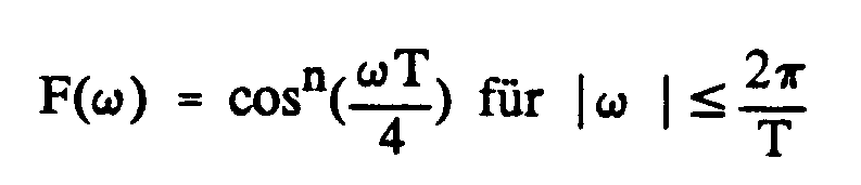
- the relation (2) can be written in the form: where the Cs i not are Newton's Binomial coefficients.
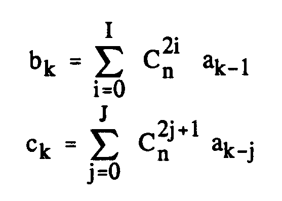
- the associated impulse response is: If the input signal is: the encoder output is: where I is the integer part of n / 2 and J is the integer part of (n-1) / 2.
- the signal r (t) can therefore be written in the form: with and
- the signal takes a finite number of states given by the alphabet of symbols b k at times kT and a finite number of states given by the alphabet of symbols c k at times kT + T / 2 .
- the proposed transmission formatting filtering class (coding associated with low-pass filtering) defines two constellations.
- the signal takes the levels of one of the constellations at times kT and the levels of the other constellation at times kT + T / 2.
- the low-pass filtering which follows the predistortion operation on transmission is not required to approach the ideal low-pass filter such as: It can be of the form: where ⁇ is a fall-back coefficient with 0 ⁇ ⁇ ⁇ 1, without destroying the zero-crossing property at times kT / 2 (with the exception of some values of k) of the impulse response of the emission formatting .
- FIG. 1 is a reminder of the representation of the constellation of a signal of MAQ64 type.
- the inputs I (in phase) and Q (in quadrature) of the modulator are independent and the symbols on each channel take their values in an alphabet ( ⁇ d, ⁇ 3d, ⁇ 5d, ⁇ 7d), where 2d is the minimum distance between two adjacent points of the constellation.
- the signal from the modulator is introduced into a power amplifier which is generally used at reduced power, that is to say in a linear part of its characteristic. At high power this amplifier is non-linear and distorts the signal in an unacceptable way. If one observes a constellation of MAQ64 type at the output of such an amplifier operating close to saturation, one observes a distorted constellation like that represented in FIG. 2A. According to the prior art, it is then sufficient to predistort in the opposite direction the constellation according to the diagram in FIG. 2B so that at the output of the amplifier the original constellation is not deformed. However, such a simple situation does not conform to reality where there is always a filtering before the power amplifier in particular to limit the band of the signal.
- the signal at the input of the modulator varies in stages once per symbol duration T.
- a predistortion circuit acting on the signal at rate 1 / T allows perfect compensation.
- the signal when the signal is filtered, it no longer varies in stages but in a continuous manner. For perfect compensation for the effect of non-linearity, it is no longer sufficient to observe the signal once per symbol duration T and to compensate for the distortion at these times.
- the curve 40 of FIG. 4A represents the impulse response of a Nyquist filter having a fallout coefficient ⁇ other than 1. This curve passes through zero at all times kT, k ⁇ 0. This kind of formatting is therefore not suitable for predistortion at the double rate of the emission of symbols.
- FIG. 4B represents the frequency response of a Nyquist filtering.
- the response is symmetrical in relation to point A (1 / 2T; 0.5) and the excess band in relation to the Nyquist band (1 / 2T) is determined by the fallout coefficient ⁇ (roll-off in English) .
- the polynomial coding followed by the low-pass filtering will have a response similar to curve 41 in the sense that it passes through zero at instants kT / 2 but with a form which can be different .
- FIG. 5 represents the part situated at the transmission of a digital transmission system provided with an adaptive predistortion circuit 50 according to the invention. It comprises an encoder 51 which, from the data a k, generates data b k and c k respectively at times kT and KT + T / 2 coded according to the invention.
- the data b k and c k respectively enter predistortion circuits 521, 522 which respectively deliver predistorted data b ′ k and c ′ k . They are added to the adder 53.
- the signal thus obtained passes through a digital-analog converter 54, a low-pass filter 55, a modulator 56 and a power amplifier 57 and is then transmitted to a transmitting antenna.
- the output of amplifier 57 is demodulated in a demodulator 58 and then filtered in a low-pass filter 59.
- the output of filter 59 is sampled by two samplers, the first 601 at kT instances and the second 60 second at instants kT + T / 2 which respectively supply the samples x (kT) and x (kT + T / 2) to two adaptation circuits 611 and 612. These compare the samples x (kT) and x (kT + T / 2) respectively with the data b k and c k .
- a conventional algorithm calculates for example the difference between the two inputs of each adaptation circuit which consequently delivers an update of the predistortion circuits.
- the most suitable method for carrying out the predistortion circuits is the use of random access memories RAM.
- a RAM will be addressed by the words b k at instants kT and its output constitutes the train of predistorted symbols b ′ k .
- the other RAM will be addressed by the words c k at times KT + T / 2 to provide the train c ′ k .
- the memories therefore contain the predistorted values of the two respective alphabets.
- FIG. 6 represents an exemplary embodiment of the coder 51. It comprises a series of I shift registers 621, 622, ... 62 I which at a given instant stores the data a k-1 , a k-2 , respectively. .. a kI on the control of the clock H.
- the set of data a k , a k-1 , ..., a kI is used to address a memory 63, for example a programmable read only memory PROM which operates the coding data a k into data b k and c k .
- random access memories 522, 522 which operate the predistortion of the data b k into data b ′ k and the data c k into data c ′ k , both in phase with the symbol clock H.
- the data b ′ K and c ′ k are then each introduced into two sets of flip-flops 641, 642 which are controlled, one 641 by the symbol clock H and the other 642 by the symbol clock inverted by an inverter 65.
- the set of flip-flops 641 delivers the data b ′ k at the instants kT either b ′ k (kT) and the set of flip-flops 642 delivers the data c ′ k at the instants kT + T / 2 or c ′ k (kT + T / 2 ).
- This digital signal r (t) passes through a digital-analog converter 54 then through the analog filter 55 which precedes the modulator.
- This filter 55 can also be a digital filter placed before the digital-analog converter 54.
- the predistortion circuit 521 is addressed by the data b k (kT)
- the predistortion circuit 522 is addressed by the data 2a k (kT), the coefficient 2 being programmed in the predistortion circuit 522.
- the two predistortion circuits 521, 522 are for example random access memories RAM which receive their update respectively from the adaptation circuits 611 and 612 (connections 701 and 702 Figure 5).
- the outputs of the predistortion circuits 521 and 522 are processed as in the case of FIG. 6 respectively by the two sets of flip-flops 641 and 642 then multiplexed by the device 53, then transmitted to the digital-analog converter 54 and to the filter 55.
- the signal transmitted by the transmitter then received at the other end of the transmission system by a receiver must on reception undergo a filtering which is determined so that overall the filtering of the transmitter associated with the filtering of the receiver corresponds to Nyquist filtering with an adequate fallout coefficient. It is this coefficient that determines the protection against interference from adjacent channels.
- a filtering which is determined so that overall the filtering of the transmitter associated with the filtering of the receiver corresponds to Nyquist filtering with an adequate fallout coefficient. It is this coefficient that determines the protection against interference from adjacent channels.
- a fallout coefficient ⁇ 0.5 in a Nyquist filtering equitably distributed between transmission and reception provides 28 dB protection.
- the overall filtering must have a lower fallout coefficient.
- the gain provided by the invention is approximately 3dB compared to previous predistortion techniques.
Landscapes
- Physics & Mathematics (AREA)
- Engineering & Computer Science (AREA)
- Nonlinear Science (AREA)
- Power Engineering (AREA)
- Algebra (AREA)
- Signal Processing (AREA)
- Computer Networks & Wireless Communication (AREA)
- General Physics & Mathematics (AREA)
- Mathematical Analysis (AREA)
- Mathematical Optimization (AREA)
- Pure & Applied Mathematics (AREA)
- Digital Transmission Methods That Use Modulated Carrier Waves (AREA)
- Reduction Or Emphasis Of Bandwidth Of Signals (AREA)
- Amplifiers (AREA)
Claims (3)
- Adaptive Vorverzerrungsschaltung (50) für ein digitales Übertragungssystem, das mit Hilfe eines Modulators (56) und eines die Daten verzerrenden Leistungsverstärkers (57) Eingangsdaten mit einer Symboltaktfrequenz T uberträgt, wobei diese Schaltung die nachfolgenden Elemente aufweist:. eine Vorverzerrungsschaltung (52₁, 52₂), welche die Eingangsdaten vor ihrem Durchgang in dem Verstärker zum Übertragen der empfangenen Eingangsdaten in entgegengesetztem Sinne vorverzerrt,. eine Anpassungsschaltung (61₁, 61₂), die ausgehend von einer Demodulation des Stromes übertragener Daten kontinuierlich die Vorverzerrungsschaltung an den Strom von Eingagsdaten anpaßt,. und ein Filter (55) zum Formen des Signals,dadurch gekennzeichnet, daß die Schaltung einen Codierer (51) aufweist, der dazu geeignet ist, auf Basis digitaler Daten ak (wobei k eine ganze Zahl ist) Folgendes zu erzeugen:. über eine erste Strecke digitale Daten bk, die in vorverzerrtem Zustand gleichphasig zu dem Symboltakt eine erste Vorverzerrungsschaltung (52₁) verlassen,. über eine zweite Strecke digitale Daten ck, die in vorverzerrtem Zustand in Gegenphase zu dem Symboltakt eine zweite Vorverzerrungsschaltung (52₂) verlassen,wobei die Signale bk und ck durch eine polynominale Codierung n. Ordnung vom Typ

und wobei J der ganze Teil von (n-1)/2 ist,
wobei die Koeffizienten C

- Adaptive Vorverzerrungsschaltung nach Anspruch 1, dadurch gekennzeichnet, daß der Codierer (51) eine Reihe von I Schieberegistern (62₁ ...62I) aufweist, in denen die Daten ak-1, ak-2, ... ak-I umlaufen, die zusammen mit den Daten ak zum Adressieren mindestens eines Speichers (63) verwendet werden, der die Codierung der Daten ak in die Daten bk und ck durchführt, wobei die Vorverzerrungsschaltungen (52₁, 52₂) Speicher mit beliebigem Zugriff sind, welche die vorverzerrten Werte zu den gleichphasigen und gegenphasigen Strecken liefern.
- Adaptive Vorverzerrungsschaltung nach Anspruch 1, dadurch gekennzeichnet, daß n = 2 ist, wodurch gilt:


Applications Claiming Priority (2)
| Application Number | Priority Date | Filing Date | Title |
|---|---|---|---|
| FR8812805A FR2637431B1 (fr) | 1988-09-30 | 1988-09-30 | Circuit de predistorsion adaptative |
| FR8812805 | 1988-09-30 |
Publications (2)
| Publication Number | Publication Date |
|---|---|
| EP0361608A1 EP0361608A1 (de) | 1990-04-04 |
| EP0361608B1 true EP0361608B1 (de) | 1993-12-01 |
Family
ID=9370568
Family Applications (1)
| Application Number | Title | Priority Date | Filing Date |
|---|---|---|---|
| EP89202405A Expired - Lifetime EP0361608B1 (de) | 1988-09-30 | 1989-09-25 | Adaptive Vorverzerrungsschaltung |
Country Status (6)
| Country | Link |
|---|---|
| US (1) | US4967164A (de) |
| EP (1) | EP0361608B1 (de) |
| JP (1) | JPH02122717A (de) |
| AU (1) | AU621785B2 (de) |
| DE (1) | DE68911097T2 (de) |
| FR (1) | FR2637431B1 (de) |
Families Citing this family (31)
| Publication number | Priority date | Publication date | Assignee | Title |
|---|---|---|---|---|
| FR2644638B1 (de) * | 1989-03-14 | 1991-05-31 | Labo Electronique Physique | |
| EP0465709A1 (de) * | 1990-07-12 | 1992-01-15 | Thomcast Ag | Verfahren zur Kompensation von Nichtlinearitäten einer Verstärkerschaltung |
| US5237332A (en) * | 1992-02-25 | 1993-08-17 | Hughes Aircraft Company | Receiver distortion correction circuit and method |
| SI9300025A (en) * | 1993-01-21 | 1994-09-30 | Spase Drakul | Digital communication system in n-dimensional vector space for transmission coded waveforms in bandlimited chanels |
| RU2142670C1 (ru) * | 1995-11-16 | 1999-12-10 | Самсунг Электроникс Ко., Лтд. | Устройство линейного усиления мощности |
| US5838195A (en) * | 1996-08-06 | 1998-11-17 | Northrop Grumman Corporation | Reduction of second order harmonic distortion in high power TWT amplifiers |
| EP0948838B1 (de) * | 1996-12-30 | 2003-08-13 | Samsung Electronics Co., Ltd. | Kombinierte lineare leistungsverstärkungsvorrichtung und verfahren |
| US5900778A (en) * | 1997-05-08 | 1999-05-04 | Stonick; John T. | Adaptive parametric signal predistorter for compensation of time varying linear and nonlinear amplifier distortion |
| JP4597100B2 (ja) * | 1997-09-05 | 2010-12-15 | 富士通株式会社 | 高周波電力増幅器用非線形補償回路 |
| US6282247B1 (en) * | 1997-09-12 | 2001-08-28 | Ericsson Inc. | Method and apparatus for digital compensation of radio distortion over a wide range of temperatures |
| FR2773423B1 (fr) * | 1998-01-06 | 2001-10-19 | Alsthom Cge Alkatel | Procede et systeme de linearisation numerique d'un amplificateur |
| GB9811381D0 (en) * | 1998-05-27 | 1998-07-22 | Nokia Mobile Phones Ltd | Predistortion control for power reduction |
| JP2000124842A (ja) * | 1998-10-14 | 2000-04-28 | Fujitsu Ltd | 伝送装置および信号点発生方法 |
| DE19850279B4 (de) * | 1998-10-30 | 2005-12-22 | Robert Bosch Gmbh | Verfahren für die Übertragung von Signalen zwischen einer ersten Funkstation und einer zweiten Funkstation und Funkstation |
| US6493400B1 (en) | 1999-04-19 | 2002-12-10 | Bae Systems Aerospace Electronics Inc. | Harmonic cancellation system |
| US6587514B1 (en) | 1999-07-13 | 2003-07-01 | Pmc-Sierra, Inc. | Digital predistortion methods for wideband amplifiers |
| US6798843B1 (en) | 1999-07-13 | 2004-09-28 | Pmc-Sierra, Inc. | Wideband digital predistortion linearizer for nonlinear amplifiers |
| US6697436B1 (en) | 1999-07-13 | 2004-02-24 | Pmc-Sierra, Inc. | Transmission antenna array system with predistortion |
| GB0107553D0 (en) * | 2001-03-27 | 2001-05-16 | Pace Micro Tech Plc | Auto-adaptive pre-distortion scheme employing parametric modelling |
| US6798849B2 (en) | 2001-12-10 | 2004-09-28 | Ibiquity Digital Corporation | AM digital audio broadcasting with analog signal pre-compensation |
| US7085330B1 (en) | 2002-02-15 | 2006-08-01 | Marvell International Ltd. | Method and apparatus for amplifier linearization using adaptive predistortion |
| US7362821B1 (en) | 2002-05-22 | 2008-04-22 | Marvel International Ltd. | Method and apparatus for amplifier linearization using adaptive predistortion |
| US6700439B2 (en) | 2002-04-11 | 2004-03-02 | Andrew Corporation | Zero-bias bypass switch |
| US6812786B2 (en) * | 2002-04-11 | 2004-11-02 | Andrew Corporation | Zero-bias bypass switching circuit using mismatched 90 degrees hybrid |
| WO2004045067A1 (ja) * | 2002-11-14 | 2004-05-27 | Hitachi Kokusai Electric Inc. | 歪み補償回路、歪み補償信号生成方法、及び電力増幅器 |
| US7680176B2 (en) * | 2005-11-21 | 2010-03-16 | Telefonaktiebolaget Lm Ericsson (Publ) | Simplified generalized rake receiver method and apparatus |
| US8498591B1 (en) | 2009-08-21 | 2013-07-30 | Marvell International Ltd. | Digital Predistortion for nonlinear RF power amplifiers |
| US8355462B2 (en) * | 2009-10-29 | 2013-01-15 | Hughes Network Systems, Llc | System and method for combined predistortion and interference cancellation in a satellite communications system |
| US8699620B1 (en) | 2010-04-16 | 2014-04-15 | Marvell International Ltd. | Digital Predistortion for nonlinear RF power amplifiers |
| US20120121036A1 (en) * | 2010-11-17 | 2012-05-17 | Cisco Technology, Inc. | Method and apparatus for clock spur suppression in direct-rf modulators |
| US9160586B1 (en) | 2013-07-24 | 2015-10-13 | Marvell International Ltd. | Method and apparatus for estimating and compensating for in-phase and quadrature (IQ) mismatch in a receiver of a wireless communication device |
Family Cites Families (3)
| Publication number | Priority date | Publication date | Assignee | Title |
|---|---|---|---|---|
| US4291277A (en) * | 1979-05-16 | 1981-09-22 | Harris Corporation | Adaptive predistortion technique for linearizing a power amplifier for digital data systems |
| US4879519A (en) * | 1988-10-31 | 1989-11-07 | American Telephone And Telegraph Company, At&T Bell Labs | Predistortion compensated linear amplifier |
| FR2652969A1 (fr) * | 1989-10-06 | 1991-04-12 | Philips Electronique Lab | Dispositif de predistorsion pour systeme de transmission numerique. |
-
1988
- 1988-09-30 FR FR8812805A patent/FR2637431B1/fr not_active Expired - Lifetime
-
1989
- 1989-09-14 US US07/407,380 patent/US4967164A/en not_active Expired - Fee Related
- 1989-09-25 DE DE68911097T patent/DE68911097T2/de not_active Expired - Fee Related
- 1989-09-25 EP EP89202405A patent/EP0361608B1/de not_active Expired - Lifetime
- 1989-09-27 JP JP1251717A patent/JPH02122717A/ja active Pending
- 1989-09-28 AU AU42334/89A patent/AU621785B2/en not_active Ceased
Also Published As
| Publication number | Publication date |
|---|---|
| DE68911097T2 (de) | 1994-05-19 |
| JPH02122717A (ja) | 1990-05-10 |
| FR2637431B1 (fr) | 1990-11-09 |
| AU4233489A (en) | 1990-04-05 |
| EP0361608A1 (de) | 1990-04-04 |
| AU621785B2 (en) | 1992-03-19 |
| US4967164A (en) | 1990-10-30 |
| DE68911097D1 (de) | 1994-01-13 |
| FR2637431A1 (fr) | 1990-04-06 |
Similar Documents
| Publication | Publication Date | Title |
|---|---|---|
| EP0361608B1 (de) | Adaptive Vorverzerrungsschaltung | |
| EP0380167B1 (de) | Adaptive Vorverzerrungsschaltung | |
| EP0421532B1 (de) | Vorverzerrungseinrichtung für digitale Übertragungssysteme | |
| EP0421533B1 (de) | Vorverzerrungseinrichtung für digitale Übertragungsysteme | |
| EP0387948B1 (de) | Adaptive Vorverzerrungsschaltung mit Speicher | |
| EP0632624A1 (de) | Datenübertragungssystem mit Vorverzerrung | |
| EP0797293B1 (de) | Verfahren zur Korrektur von nichtlinearen Verzerrungen in einem Verstärker und ein solches Verfahren verwendenden Funksenders | |
| EP0929148A1 (de) | Verfahren und Vorrichtung zur numerischen Linearisierung eines Verstärkers | |
| EP0329537B1 (de) | Übertragungssystem mit MSK-Modulation und kohärenter differentieller Detektion | |
| EP0125722A1 (de) | Schaltungsanordnung zur kombinierten adaptativen Entzerrung und Demodulation | |
| FR2746564A1 (fr) | Procede pour corriger des non-linearites d'un amplificateur, et emetteur radio mettant en oeuvre un tel procede | |
| EP1878185B1 (de) | Verfahren zur Kodierung eines OFDM/OQAM-Signals unter Verwendung von Symbolen mit komplexen Werten und entsprechendes Signal, Einrichtungen und Computerprogramme | |
| EP0352159B1 (de) | Frequenzabweichungstolerierendes Verfahren und Vorrichtung zur Demodulation von, durch eine Binärsymbolreihe, winkelmodulierten Signalen mit konstanter Umhüllung und kontinuierlicher Phase | |
| EP0792053A1 (de) | Digitales Übertragungssystem zur Übertragung mittels kontinuierlicher Phasenmodulation | |
| EP2504963B1 (de) | System und verfahren zum senden und zum empfangen eines digitalen funksignals | |
| EP2963881B1 (de) | Verbessertes verfahren der kontinuierlichen phasenmodulation, und sender zur umsetzung dieses verfahrens | |
| EP1044543A1 (de) | Modulation für ein digitales schmalbandsignal und nahezu konstanter hüllkurve | |
| FR2885471A1 (fr) | Procede de decodage iteratif d'un signal ofdm/oqam utilisant des symboles a valeurs complexes, dispositif et programme d'ordinateur correspondants | |
| EP1354453B1 (de) | Verfahren zur übertragung und zum empfang eines synchronen modulierten biorthogonalen merhträgersignales, sowie vorrichtungen zur übertragung und zum empfang dafür | |
| FR2675001A1 (fr) | Procede et dispositif de modulation numerique a composantes en phase et en quadrature et installation de transmission en comportant application. | |
| EP0896456B1 (de) | Pulsformung für die Kontrolle von Amplitudenvariationen von PSK-Signalen | |
| EP1478146A1 (de) | Empfang zweier unkorrelierter, auf einem einzigen Kanal übertragender Signale | |
| EP0120774B1 (de) | Phasengesteuerter Winkelmodulationsmodem für binäre Datensignale | |
| WO2006114513A1 (fr) | Procede de transmission d'un signal module avec une forte dynamique d'amplitude, emetteur et recepteur correspondant |
Legal Events
| Date | Code | Title | Description |
|---|---|---|---|
| PUAI | Public reference made under article 153(3) epc to a published international application that has entered the european phase |
Free format text: ORIGINAL CODE: 0009012 |
|
| AK | Designated contracting states |
Kind code of ref document: A1 Designated state(s): DE FR GB IT SE |
|
| 17P | Request for examination filed |
Effective date: 19901002 |
|
| 17Q | First examination report despatched |
Effective date: 19930108 |
|
| GRAA | (expected) grant |
Free format text: ORIGINAL CODE: 0009210 |
|
| AK | Designated contracting states |
Kind code of ref document: B1 Designated state(s): DE FR GB IT SE |
|
| REF | Corresponds to: |
Ref document number: 68911097 Country of ref document: DE Date of ref document: 19940113 |
|
| ITF | It: translation for a ep patent filed | ||
| GBT | Gb: translation of ep patent filed (gb section 77(6)(a)/1977) |
Effective date: 19940221 |
|
| PG25 | Lapsed in a contracting state [announced via postgrant information from national office to epo] |
Ref country code: SE Effective date: 19940926 |
|
| PLBE | No opposition filed within time limit |
Free format text: ORIGINAL CODE: 0009261 |
|
| STAA | Information on the status of an ep patent application or granted ep patent |
Free format text: STATUS: NO OPPOSITION FILED WITHIN TIME LIMIT |
|
| 26N | No opposition filed | ||
| EAL | Se: european patent in force in sweden |
Ref document number: 89202405.0 |
|
| ITPR | It: changes in ownership of a european patent |
Owner name: CAMBIO RAGIONE SOCIALE;PHILIPS ELECTRONICS N.V. |
|
| EUG | Se: european patent has lapsed |
Ref document number: 89202405.0 |
|
| REG | Reference to a national code |
Ref country code: FR Ref legal event code: CJ Ref country code: FR Ref legal event code: CD |
|
| PGFP | Annual fee paid to national office [announced via postgrant information from national office to epo] |
Ref country code: GB Payment date: 19970829 Year of fee payment: 9 |
|
| PGFP | Annual fee paid to national office [announced via postgrant information from national office to epo] |
Ref country code: FR Payment date: 19970923 Year of fee payment: 9 |
|
| PGFP | Annual fee paid to national office [announced via postgrant information from national office to epo] |
Ref country code: DE Payment date: 19971121 Year of fee payment: 9 |
|
| PG25 | Lapsed in a contracting state [announced via postgrant information from national office to epo] |
Ref country code: GB Free format text: LAPSE BECAUSE OF NON-PAYMENT OF DUE FEES Effective date: 19980925 |
|
| GBPC | Gb: european patent ceased through non-payment of renewal fee |
Effective date: 19980925 |
|
| PG25 | Lapsed in a contracting state [announced via postgrant information from national office to epo] |
Ref country code: FR Free format text: LAPSE BECAUSE OF NON-PAYMENT OF DUE FEES Effective date: 19990531 |
|
| PG25 | Lapsed in a contracting state [announced via postgrant information from national office to epo] |
Ref country code: DE Free format text: LAPSE BECAUSE OF NON-PAYMENT OF DUE FEES Effective date: 19990701 |
|
| REG | Reference to a national code |
Ref country code: FR Ref legal event code: ST |
|
| PG25 | Lapsed in a contracting state [announced via postgrant information from national office to epo] |
Ref country code: IT Free format text: LAPSE BECAUSE OF NON-PAYMENT OF DUE FEES Effective date: 20050925 |