EP0930666A1 - Filtre diélectrique et duplexeur diélectrique - Google Patents
Filtre diélectrique et duplexeur diélectrique Download PDFInfo
- Publication number
- EP0930666A1 EP0930666A1 EP99100831A EP99100831A EP0930666A1 EP 0930666 A1 EP0930666 A1 EP 0930666A1 EP 99100831 A EP99100831 A EP 99100831A EP 99100831 A EP99100831 A EP 99100831A EP 0930666 A1 EP0930666 A1 EP 0930666A1
- Authority
- EP
- European Patent Office
- Prior art keywords
- dielectric
- electric probe
- covering
- filter
- electric
- Prior art date
- Legal status (The legal status is an assumption and is not a legal conclusion. Google has not performed a legal analysis and makes no representation as to the accuracy of the status listed.)
- Granted
Links
- 239000000523 sample Substances 0.000 claims abstract description 81
- 230000008878 coupling Effects 0.000 claims abstract description 43
- 238000010168 coupling process Methods 0.000 claims abstract description 43
- 238000005859 coupling reaction Methods 0.000 claims abstract description 43
- 230000013011 mating Effects 0.000 claims description 5
- 239000011347 resin Substances 0.000 description 32
- 229920005989 resin Polymers 0.000 description 32
- 239000003989 dielectric material Substances 0.000 description 15
- 229910052751 metal Inorganic materials 0.000 description 9
- 239000002184 metal Substances 0.000 description 9
- 230000008859 change Effects 0.000 description 6
- 229910000679 solder Inorganic materials 0.000 description 4
- BQCADISMDOOEFD-UHFFFAOYSA-N Silver Chemical compound [Ag] BQCADISMDOOEFD-UHFFFAOYSA-N 0.000 description 2
- 239000000919 ceramic Substances 0.000 description 2
- 230000009467 reduction Effects 0.000 description 2
- 230000035939 shock Effects 0.000 description 2
- 229910052709 silver Inorganic materials 0.000 description 2
- 239000004332 silver Substances 0.000 description 2
- 229910010293 ceramic material Inorganic materials 0.000 description 1
- 239000011248 coating agent Substances 0.000 description 1
- 238000000576 coating method Methods 0.000 description 1
- 230000007774 longterm Effects 0.000 description 1
- 238000000034 method Methods 0.000 description 1
- 230000008569 process Effects 0.000 description 1
- 239000000126 substance Substances 0.000 description 1
- 239000010409 thin film Substances 0.000 description 1
Images


Classifications
-
- H—ELECTRICITY
- H03—ELECTRONIC CIRCUITRY
- H03H—IMPEDANCE NETWORKS, e.g. RESONANT CIRCUITS; RESONATORS
- H03H9/00—Networks comprising electromechanical or electro-acoustic elements; Electromechanical resonators
- H03H9/30—Time-delay networks
-
- H—ELECTRICITY
- H01—ELECTRIC ELEMENTS
- H01P—WAVEGUIDES; RESONATORS, LINES, OR OTHER DEVICES OF THE WAVEGUIDE TYPE
- H01P1/00—Auxiliary devices
- H01P1/20—Frequency-selective devices, e.g. filters
- H01P1/207—Hollow waveguide filters
- H01P1/208—Cascaded cavities; Cascaded resonators inside a hollow waveguide structure
- H01P1/2084—Cascaded cavities; Cascaded resonators inside a hollow waveguide structure with dielectric resonators
-
- H—ELECTRICITY
- H01—ELECTRIC ELEMENTS
- H01P—WAVEGUIDES; RESONATORS, LINES, OR OTHER DEVICES OF THE WAVEGUIDE TYPE
- H01P5/00—Coupling devices of the waveguide type
- H01P5/04—Coupling devices of the waveguide type with variable factor of coupling
Definitions
- the present invention relates to a dielectric filter and a dielectric duplexer for use in a communication base station or the like.
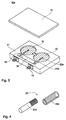
- FIG. 7 A dielectric filter relating to the present invention is shown in Fig. 7. Although this dielectric filter is described in copending U. S. Pat. Application No. 924040, this dielectric filter was not known yet in the art at the time when the invention, on the basis of which the priority of the present invention is claimed, was filed as Japanese Patent Application No. H-10-8860.
- Fig. 7 is a perspective view of the dielectric filter 110.
- an upper lid 114 is removed so that the internal structure can be seen.
- the dielectric filter shown herein is, by way of example, of the two-stage band-rejection filter type including two disk-shaped dielectrics 112 disposed side by side in a shielding cavity frame 111.
- the dielectric filter 110 includes a shielding cavity frame 111 formed of metal, a dielectric 112 disposed in the shielding cavity frame 111, and external coupling means 120.
- the dielectric 112 is formed of ceramic in a disk shape and electrodes are formed of silver or the like on two opposite upper and lower surfaces thereof. The lower surface of the dielectric 112 is fixed via solder or the like to the inner bottom surface of the shielding cavity frame 111 thereby achieving electric connection.
- the external coupling means 120 includes an electric probe 121 made of a metal wire. The electric probe 121 is disposed in such a manner that it extends in a space between the upper surface of the dielectric 112 and the shielding cavity frame 111 without having contact with either the dielectric 112 or the shielding cavity frame 111.
- the electric probe 121 is connected via solder to an external connector 113 attached to the shielding cavity frame 111 so that a signal is input and output via the electric probe 121. That is, a signal is supplied via a cable connected to the external connector 113 and is passed through the electric probe 121.
- the electric probe 121 is coupled with the dielectric 112 via capacitance created between the electric probe 121 and the electrode of the dielectric 112.
- the dielectric 112 coupled with the electric probe 121 has resonance and thus serves as a band-rejection filter.
- the resultant signal is output through a cable connected to another external connector 113.
- the coupling between the electric probe and the dielectric is realized via the capacitance between the electric probe and the dielectric.
- the capacitance is determined by the distance between the electric probe and the dielectric, the areas of surfaces facing each other, and the dielectric constant of a substance existing between them.
- the attenuation varies with the change in the strength of the coupling, and the characteristic of the dielectric filter vary in such a manner that the filter has a band-rejection or bandpass characteristic with a wide bandwidth when the coupling is strong while the bandwidth becomes narrow when the coupling is weak. Therefore, to achieve a dielectric filter having desired characteristics, it is required to adjust the coupling between the electric probe and the dielectric. That is, it is required to adjust the capacitance between the electric probe and the dielectric.
- the electric probe made of a metal wire is used as the external coupling means.
- the capacitance may be varied, as described above, by varying the distance between the electric probe and the dielectric, the areas of the surfaces, and/or the dielectric constant.
- it is difficult to change the location of the electric probe connected to the external connector because it is difficult to change the location of the external connector attached to the shielding cavity frame.
- the dielectric constant of air is impossible to change.
- a most practical manner of adjusting the capacitance between the electric probe and the dielectric is to change the length of the electric probe thereby changing the areas of the surfaces facing each other.
- an electrical discharge occurs through air existing between the electric probe and the dielectric when the potential difference between them exceeds the dielectric strength of air. Such a discharge can cause a difference in the characteristic of the electrode or the electric probe of the dielectric filter.
- a dielectric filter including a shielding cavity frame having electric conductivity, a dielectric having electrodes formed on two opposing faces and disposed in the shielding cavity frame, and external coupling means, wherein the external coupling means includes an electric probe at least a part of which is covered with a covering dielectric.
- the covering dielectric covering the electric probe is preferably movable.
- the movability of the covering dielectric may be achieved by connecting the covering dielectric to the electric probe by means of mating via screw threads.
- a dielectric duplexer including a shielding cavity frame having electric conductivity, a dielectric having electrodes formed on two opposing faces and disposed in the shielding cavity frame, external coupling means, input/output connection means and antenna connection means connected to the coupling means, wherein the external coupling means includes an electric probe at least a part of which is covered with a covering dielectric.
- the covering dielectric covering the electric probe is preferably movable.
- the movability of the covering dielectric may be achieved by connecting the covering dielectric to the electric probe by means of mating via screw threads.
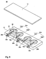
- FIG. 1 is a perspective view of the dielectric filter 10 according to the present invention. In the figure, an upper lid 14 is removed so that the internal structure can be seen.
- the dielectric filter 10 includes a shielding cavity frame 11, disk-shaped dielectrics 12, and external coupling means 20.
- the shielding cavity frame 11 is formed of metal and external connectors 13 are attached to it so that a signal is input and output from and to the outside via cables.
- the external coupling means 20 are connected to the respective external connectors 13 via solder.
- Each dielectric 12 is formed of ceramic in a disk shape and electrodes are formed on it by means of coating and baking silver paste on two opposing surfaces. The lower surface of each dielectric 12 is fixed via solder or the like to the inner bottom face of the shielding cavity frame 11 thereby achieving electric connection.
- the dielectric 12 may be soldered to a ground plate or the like and may be placed in the shielding cavity frame 11.
- two dielectrics 12 are placed side by side and these two dielectrics 12 are connected to each other via a 1/4-transmission line 15 so that the dielectric filter 10 acts as a two-stage band-rejection filter.
- the shielding cavity frame 11 may also be produced by forming an electrically conductive layer on the surface of a ceramic material.
- the dielectric 12 may also be formed into a square shape.
- the electrodes on the two opposing surfaces of the dielectric 12 may be formed into the structure of a multilayer thin film so as to reduce the loss.
- the external coupling means 20 includes an electric probe 21 made up of a metal wire a desired part of which is covered with a resin or the like 22 serving as a covering dielectric.
- a resin or the like 22 serving as a covering dielectric.
- the resin 22 is formed into the shape of a cylinder with a diameter greater than the diameter of the electric probe 21 wherein a through-hole is formed such that it extends from one end of the cylinder to the opposite end or a semi-through-hole is formed such that one end of the semi-through-hole is closed with one end of the cylinder.
- the electric probe 21 is inserted into this hole and the resin 22 is moved to a desired position so that a desired part of the electric probe 21 is covered with the resin 22 as shown in Fig. 2.
- the resin 22 is present between the electric probe 21 and the dielectric 12.
- the resin 22 has a higher dielectric strength and a greater dielectric constant than air. Therefore, covering the electric probe 21 with the resin 22 results in a reduction in the probability that a discharge will occur between the electric probe 21 and the dielectric 12.
- the capacitance can be varied by varying the dielectric constant between the electric probe 21 and the dielectric 12 using the resin 22.
- the dielectric filter of the present embodiment includes two disk-shaped dielectrics 12 each having electrodes formed on two opposing surfaces and disposed side by side in a shielding cavity frame 11.
- the two dielectrics 12 are coupled to each other via a capacitive coupling member 16.
- the dielectric filter 10a having the structure described above acts as a two-stage bandpass filter.
- Fig. 4 is a perspective view illustrating an electric probe 21a made up of a metal wire and also illustrating a resin 22a covering the electric probe 21a, according to the present embodiment.
- the electric probe 21a and the resin 22a are threaded such that the electric probe 21a serves as a male screw and the resin 22a acts as a female screw.
- the resin 22a is screwed onto the electric probe 21a thereby connecting them to each other. This allows the resin 22a to be easily connected to the electric probe 21a in a firm fashion so that the resin 22a is not moved by external vibrations or a mechanical shock. That is, the strength of the coupling between the electric probe 21a and the dielectric 12 is not changed by an external disturbance.
- a third embodiment of the present invention is described below. Also in this figure, an upper lid 14 is removed so that the internal structure of a dielectric filter 10b can be seen. As in the first embodiment, two disk-shaped dielectrics 12 are connected to each other via a /4-transmission line 15 so that the dielectric filter 10b acts as a two-stage band-rejection filter. Similar parts to those in the previous embodiments are denoted by similar reference numerals and they are not described in further detail herein.
- each external coupling means 20 includes an electric probe 21b made up of a metal wire a desired part of which is covered with a resin or the like 22b serving as a covering dielectric.
- a resin or the like 22b serving as a covering dielectric.
- the resin 22b polyprene or a similar resin is employed which can be easily formed into a desired shape and which has elasticity which makes it easy to perform the adjustment which will be described later.
- This resin 22b has a hole corresponding to the electric probe 21b. The electric probe 21b is inserted into the hole and the resin 22b is moved to a desired position so that a desired part of the electric probe 21b is covered with the resin 22b. Thus, the resin 22b is present between the electric probe 21b and the dielectric 12.
- the resin 22b has a higher dielectric strength and a greater dielectric constant than air. Therefore, covering each electric probe 21b with the resin 22b results in a reduction in the probability that a discharge will occur between the electric probe 21b and the dielectric 12. Furthermore, the capacitance can be varied by varying the dielectric constant between the electric probe 21b and the dielectric 12 using the resin 22b. More specifically, by varying the relative length of the part of the electric probe 21b inserted in the resin 22b, it is possible to vary the capacitance and thus the strength of the coupling between the electric probe 21b and the dielectric 12. Thus, it is possible to make an adjustment such that the dielectric filter has desired characteristics. Because the external coupling means 20 is formed into the shape of a plate, it is easier to obtain desired capacitance than in the first embodiment.
- FIG. 6 an embodiment of a dielectric duplexer according to the present invention is described below. Similar parts to those in the previous embodiments are denoted by similar reference numerals and they are not described in further detail herein.
- a dielectric duplexer 30 includes a first dielectric filter 31a and a second dielectric filter 31b wherein the first dielectric filter 31 includes two disk-shaped dielectrics 12a1 and 12a2 disposed in a shielding cavity frame 11 and the second dielectric filter 31 includes two disk-shaped dielectrics 12b1 and 12b2.
- the two dielectrics 12a1 and 12a2 of the first dielectric filter 31a are coupled to each other via a capacitive coupling member 16a so that the first dielectric filter 31a serves as a transmitting bandpass filter.
- the two dielectrics 12b1 and 12b2 of the second dielectric filter 31a have resonant frequencies different from those of the dielectrics 12a1 and 12a2 of the first dielectric filter 31a and are coupled to each other via a capacitive coupling member 16b so that the second dielectric filter 31b serves as a receiving bandpass filter.
- the external coupling means 20a coupled with the dielectric 12a1 of the first dielectric filter 31a is connected to an external connector 13a which is connected to an external transmitting circuit.
- the external coupling means 20d coupled with the dielectric 12b2 of the second dielectric filter 31b is connected to an external connector 13b which is connected to an external receiving circuit.
- the external coupling means 20b coupled with the dielectric 12a2 of the first dielectric filter 31a and the external coupling means 20c coupled with the dielectric 12b1 of the second dielectric filter 31b are connected to an external connector 13c which is connected to an external antenna.
- the external coupling means 20a, 20b, 20c, and 20d each include an electric probe 21 made up of a metal wire a desired part of which is covered with a resin or the like 22 serving as a covering dielectric.
- a resin or the like 22 serving as a covering dielectric.
- the capacitance can be varied by varying the dielectric constant between the electric probe 21s and the dielectrics 12a1, 12a2, 12b1, and 12b2, using the resins 22.
- the present invention has various advantages. That is, in the present invention, the electric probe made of metal and serving as the external coupling means in the dielectric filter or dielectric duplexer is covered with the covering dielectric thereby increasing the dielectric strength between the electric probe and the dielectric thus reducing the probability that a discharge will occur.
- the covering dielectric on the electric probe is provided in a movable fashion whereby the part of the electric probe covered with the covering dielectric can be varied. This makes it possible to easily adjust the strength of the coupling between the electric probe and the dielectric without having to cut each electric probe to a shorter length. That is, by varying the coupling strength, it is possible to make an adjustment such that the pass band or the rejection band of the dielectric filter or the dielectric duplexer has a greater or smaller bandwidth as required. Thus, it is possible to easily produce dielectric filters and dielectric duplexers having desired characteristics depending on applications in which they are used.
- the covering dielectric to the electric probe by means of mating via screw threads, it becomes possible to prevent the length of the part of the electric probe covered with the covering dielectric from varying after completion of the characteristic adjustment. That is, after adjusting the characteristics of the dielectric filter, the position of the covering dielectric on the electric probe is not varied by an external shock or vibrations. Thus, it is possible to prevent the dielectric filter and the dielectric duplexer from having a change in characteristics due to an external disturbance.
- the present invention provides a dielectric filter and a dielectric duplexer whose characteristics can be easily adjusted and which have good long-term reliability.
Landscapes
- Physics & Mathematics (AREA)
- Acoustics & Sound (AREA)
- Control Of Motors That Do Not Use Commutators (AREA)
Applications Claiming Priority (2)
| Application Number | Priority Date | Filing Date | Title |
|---|---|---|---|
| JP10008860A JPH11205004A (ja) | 1998-01-20 | 1998-01-20 | 誘電体フィルタおよび誘電体デュプレクサ |
| JP886098 | 1998-01-20 |
Publications (2)
| Publication Number | Publication Date |
|---|---|
| EP0930666A1 true EP0930666A1 (fr) | 1999-07-21 |
| EP0930666B1 EP0930666B1 (fr) | 2006-08-09 |
Family
ID=11704469
Family Applications (1)
| Application Number | Title | Priority Date | Filing Date |
|---|---|---|---|
| EP99100831A Expired - Lifetime EP0930666B1 (fr) | 1998-01-20 | 1999-01-18 | Filtre diélectrique et duplexeur diélectrique |
Country Status (10)
| Country | Link |
|---|---|
| US (1) | US6218914B1 (fr) |
| EP (1) | EP0930666B1 (fr) |
| JP (1) | JPH11205004A (fr) |
| KR (1) | KR100317923B1 (fr) |
| CN (1) | CN1121732C (fr) |
| BR (1) | BR9900664A (fr) |
| CA (1) | CA2259696C (fr) |
| DE (1) | DE69932653T2 (fr) |
| NO (1) | NO320338B1 (fr) |
| TW (1) | TW439317B (fr) |
Cited By (2)
| Publication number | Priority date | Publication date | Assignee | Title |
|---|---|---|---|---|
| EP1315228A4 (fr) * | 2000-08-29 | 2004-03-17 | Matsushita Electric Industrial Co Ltd | Filtre dielectrique |
| EP3598568A1 (fr) * | 2018-07-20 | 2020-01-22 | The Boeing Company | Sonde réglable pour filtres rf interconnectés hautes performances |
Families Citing this family (9)
| Publication number | Priority date | Publication date | Assignee | Title |
|---|---|---|---|---|
| CN101098035B (zh) * | 2006-06-29 | 2010-05-26 | 奥雷通光通讯设备(上海)有限公司 | 一种波导天线口金属棒耦合结构 |
| CN101098034B (zh) * | 2006-06-29 | 2010-05-26 | 奥雷通光通讯设备(上海)有限公司 | 一种波导天线口金属环耦合结构 |
| JP4923975B2 (ja) * | 2006-11-21 | 2012-04-25 | ソニー株式会社 | 通信システム並びに通信装置 |
| CN101471471B (zh) * | 2007-12-27 | 2012-11-28 | 奥雷通光通讯设备(上海)有限公司 | 波导天线口金属片耦合结构 |
| CN102004173B (zh) * | 2009-09-01 | 2014-02-19 | 鸿富锦精密工业(深圳)有限公司 | 探针 |
| CN101894994A (zh) * | 2010-07-13 | 2010-11-24 | 江苏贝孚德通讯科技股份有限公司 | 一种带阻滤波器 |
| CN104577275B (zh) * | 2015-01-16 | 2017-08-25 | 华南理工大学 | 基于同轴馈电探针微扰的多模腔体谐振器的宽带滤波器 |
| CN104900951B (zh) * | 2015-04-08 | 2018-06-05 | 华为技术有限公司 | 介质滤波器和通信设备 |
| CN110931954B (zh) * | 2019-11-20 | 2022-04-12 | 武汉凡谷电子技术股份有限公司 | 一种高互调的afu天线 |
Citations (4)
| Publication number | Priority date | Publication date | Assignee | Title |
|---|---|---|---|---|
| US2431941A (en) * | 1943-11-29 | 1947-12-02 | Rca Corp | Microwave coupling device |
| JPS58218201A (ja) * | 1982-06-11 | 1983-12-19 | Alps Electric Co Ltd | マイクロ波受信機 |
| US4727342A (en) * | 1985-09-24 | 1988-02-23 | Murata Manufacturing Co., Ltd. | Dielectric resonator |
| JPH02285702A (ja) * | 1989-04-26 | 1990-11-26 | Matsushita Electric Ind Co Ltd | 導波管―マイクロストリップ線路変換装置 |
Family Cites Families (2)
| Publication number | Priority date | Publication date | Assignee | Title |
|---|---|---|---|---|
| US4740764A (en) * | 1987-06-03 | 1988-04-26 | Varian Associates, Inc. | Pressure sealed waveguide to coaxial line connection |
| JP3087664B2 (ja) * | 1996-11-06 | 2000-09-11 | 株式会社村田製作所 | 誘電体共振器装置及び高周波モジュール |
-
1998
- 1998-01-20 JP JP10008860A patent/JPH11205004A/ja active Pending
-
1999
- 1999-01-15 TW TW088100597A patent/TW439317B/zh not_active IP Right Cessation
- 1999-01-18 EP EP99100831A patent/EP0930666B1/fr not_active Expired - Lifetime
- 1999-01-18 DE DE69932653T patent/DE69932653T2/de not_active Expired - Lifetime
- 1999-01-18 KR KR1019990001227A patent/KR100317923B1/ko not_active Expired - Lifetime
- 1999-01-18 BR BR9900664-2A patent/BR9900664A/pt not_active IP Right Cessation
- 1999-01-19 CA CA002259696A patent/CA2259696C/fr not_active Expired - Lifetime
- 1999-01-19 NO NO19990238A patent/NO320338B1/no not_active IP Right Cessation
- 1999-01-20 US US09/233,521 patent/US6218914B1/en not_active Expired - Lifetime
- 1999-01-20 CN CN99101363A patent/CN1121732C/zh not_active Expired - Lifetime
Patent Citations (4)
| Publication number | Priority date | Publication date | Assignee | Title |
|---|---|---|---|---|
| US2431941A (en) * | 1943-11-29 | 1947-12-02 | Rca Corp | Microwave coupling device |
| JPS58218201A (ja) * | 1982-06-11 | 1983-12-19 | Alps Electric Co Ltd | マイクロ波受信機 |
| US4727342A (en) * | 1985-09-24 | 1988-02-23 | Murata Manufacturing Co., Ltd. | Dielectric resonator |
| JPH02285702A (ja) * | 1989-04-26 | 1990-11-26 | Matsushita Electric Ind Co Ltd | 導波管―マイクロストリップ線路変換装置 |
Non-Patent Citations (3)
| Title |
|---|
| A.B. BERESKIN: "MULTI-SCREW TUNER FOR ANY MISMATCH", MICROWAVE JOURNAL., vol. 26, no. 8, August 1983 (1983-08-01), DEDHAM US, pages 133 - 141, XP002099367 * |
| PATENT ABSTRACTS OF JAPAN vol. 15, no. 58 (E - 1032) 12 February 1991 (1991-02-12) * |
| PATENT ABSTRACTS OF JAPAN vol. 8, no. 70 (E - 235) 3 April 1984 (1984-04-03) * |
Cited By (3)
| Publication number | Priority date | Publication date | Assignee | Title |
|---|---|---|---|---|
| EP1315228A4 (fr) * | 2000-08-29 | 2004-03-17 | Matsushita Electric Industrial Co Ltd | Filtre dielectrique |
| EP3598568A1 (fr) * | 2018-07-20 | 2020-01-22 | The Boeing Company | Sonde réglable pour filtres rf interconnectés hautes performances |
| US10985435B2 (en) | 2018-07-20 | 2021-04-20 | The Boeing Company | Tunable probe for high-performance cross-coupled RF filters |
Also Published As
| Publication number | Publication date |
|---|---|
| CA2259696C (fr) | 2002-06-25 |
| CA2259696A1 (fr) | 1999-07-20 |
| NO990238D0 (no) | 1999-01-19 |
| CN1121732C (zh) | 2003-09-17 |
| KR19990067955A (ko) | 1999-08-25 |
| KR100317923B1 (ko) | 2001-12-22 |
| JPH11205004A (ja) | 1999-07-30 |
| US6218914B1 (en) | 2001-04-17 |
| TW439317B (en) | 2001-06-07 |
| EP0930666B1 (fr) | 2006-08-09 |
| CN1238571A (zh) | 1999-12-15 |
| DE69932653T2 (de) | 2006-12-14 |
| BR9900664A (pt) | 1999-12-21 |
| NO990238L (no) | 1999-07-21 |
| NO320338B1 (no) | 2005-11-21 |
| DE69932653D1 (de) | 2006-09-21 |
Similar Documents
| Publication | Publication Date | Title |
|---|---|---|
| AU555342B2 (en) | Ceramic bandpass filter | |
| EP1024548B1 (fr) | Filtre diélectrique | |
| US5905420A (en) | Dielectric filter | |
| KR100327912B1 (ko) | 대역저지 유전체 필터, 유전체 듀플렉서 및 이를 사용한 통신장치 | |
| US4607242A (en) | Microwave filter | |
| US5365209A (en) | Dielectric filters and duplexers incorporating same | |
| US6218914B1 (en) | Dielectric filter and dielectric duplexer including a movable probe | |
| CN109672011B (zh) | 天线及其介质波导滤波器 | |
| CA2030136C (fr) | Filtre a elements ceramiques dote de broches d'accouplement cuites simultanement | |
| JPS638641B2 (fr) | ||
| US5374906A (en) | Filter device for transmitter-receiver antenna | |
| US10581131B2 (en) | Ceramic filter with differential conductivity | |
| US6211755B1 (en) | Dielectric resonator, dielectric filter, dielectric duplexer, communication device, and method of producing dielectric resonator | |
| CN1949588B (zh) | 电介质装置 | |
| GB2284942A (en) | Dielectric resonator and filter | |
| JPH03195102A (ja) | マイクロ波導波管用帯域消去フィルタ | |
| US5170141A (en) | Ceramic filter | |
| JPH0221162B2 (fr) | ||
| KR20030013605A (ko) | 공동형 대역저지 여파기 | |
| JP3212805B2 (ja) | 誘電セラミックフィルター | |
| JPH055682Y2 (fr) | ||
| JPH01181203A (ja) | 誘電体共振器 | |
| JPH0389602A (ja) | 誘電体フィルタの通過帯域調整方法 | |
| JPH048644Y2 (fr) | ||
| JPH0865010A (ja) | 広帯域誘電体フィルタ |
Legal Events
| Date | Code | Title | Description |
|---|---|---|---|
| PUAI | Public reference made under article 153(3) epc to a published international application that has entered the european phase |
Free format text: ORIGINAL CODE: 0009012 |
|
| 17P | Request for examination filed |
Effective date: 19990118 |
|
| AK | Designated contracting states |
Kind code of ref document: A1 Designated state(s): DE FI FR GB IT NL SE |
|
| AX | Request for extension of the european patent |
Free format text: AL;LT;LV;MK;RO;SI |
|
| AKX | Designation fees paid |
Free format text: DE FI FR GB IT NL SE |
|
| 17Q | First examination report despatched |
Effective date: 20040810 |
|
| GRAP | Despatch of communication of intention to grant a patent |
Free format text: ORIGINAL CODE: EPIDOSNIGR1 |
|
| GRAS | Grant fee paid |
Free format text: ORIGINAL CODE: EPIDOSNIGR3 |
|
| GRAA | (expected) grant |
Free format text: ORIGINAL CODE: 0009210 |
|
| AK | Designated contracting states |
Kind code of ref document: B1 Designated state(s): DE FI FR GB IT NL SE |
|
| PG25 | Lapsed in a contracting state [announced via postgrant information from national office to epo] |
Ref country code: NL Free format text: LAPSE BECAUSE OF FAILURE TO SUBMIT A TRANSLATION OF THE DESCRIPTION OR TO PAY THE FEE WITHIN THE PRESCRIBED TIME-LIMIT Effective date: 20060809 Ref country code: IT Free format text: LAPSE BECAUSE OF FAILURE TO SUBMIT A TRANSLATION OF THE DESCRIPTION OR TO PAY THE FEE WITHIN THE PRE;WARNING: LAPSES OF ITALIAN PATENTS WITH EFFECTIVE DATE BEFORE 2007 MAY HAVE OCCURRED AT ANY TIME BEFORE 2007. THE CORRECT EFFECTIVE DATE MAY BE DIFFERENT FROM THE ONE RECORDED.SCRIBED TIME-LIMIT Effective date: 20060809 Ref country code: FI Free format text: LAPSE BECAUSE OF FAILURE TO SUBMIT A TRANSLATION OF THE DESCRIPTION OR TO PAY THE FEE WITHIN THE PRESCRIBED TIME-LIMIT Effective date: 20060809 |
|
| REG | Reference to a national code |
Ref country code: GB Ref legal event code: FG4D |
|
| REF | Corresponds to: |
Ref document number: 69932653 Country of ref document: DE Date of ref document: 20060921 Kind code of ref document: P |
|
| PG25 | Lapsed in a contracting state [announced via postgrant information from national office to epo] |
Ref country code: SE Free format text: LAPSE BECAUSE OF FAILURE TO SUBMIT A TRANSLATION OF THE DESCRIPTION OR TO PAY THE FEE WITHIN THE PRESCRIBED TIME-LIMIT Effective date: 20061109 |
|
| NLV1 | Nl: lapsed or annulled due to failure to fulfill the requirements of art. 29p and 29m of the patents act | ||
| ET | Fr: translation filed | ||
| PLBE | No opposition filed within time limit |
Free format text: ORIGINAL CODE: 0009261 |
|
| STAA | Information on the status of an ep patent application or granted ep patent |
Free format text: STATUS: NO OPPOSITION FILED WITHIN TIME LIMIT |
|
| 26N | No opposition filed |
Effective date: 20070510 |
|
| REG | Reference to a national code |
Ref country code: FR Ref legal event code: PLFP Year of fee payment: 18 |
|
| REG | Reference to a national code |
Ref country code: FR Ref legal event code: PLFP Year of fee payment: 19 |
|
| REG | Reference to a national code |
Ref country code: FR Ref legal event code: PLFP Year of fee payment: 20 |
|
| PGFP | Annual fee paid to national office [announced via postgrant information from national office to epo] |
Ref country code: GB Payment date: 20180119 Year of fee payment: 20 Ref country code: DE Payment date: 20180122 Year of fee payment: 20 |
|
| PGFP | Annual fee paid to national office [announced via postgrant information from national office to epo] |
Ref country code: FR Payment date: 20180119 Year of fee payment: 20 |
|
| REG | Reference to a national code |
Ref country code: DE Ref legal event code: R071 Ref document number: 69932653 Country of ref document: DE |
|
| REG | Reference to a national code |
Ref country code: GB Ref legal event code: PE20 Expiry date: 20190117 |
|
| PG25 | Lapsed in a contracting state [announced via postgrant information from national office to epo] |
Ref country code: GB Free format text: LAPSE BECAUSE OF EXPIRATION OF PROTECTION Effective date: 20190117 |