EP0930678A2 - Transmetteur optique - Google Patents
Transmetteur optique Download PDFInfo
- Publication number
- EP0930678A2 EP0930678A2 EP99100367A EP99100367A EP0930678A2 EP 0930678 A2 EP0930678 A2 EP 0930678A2 EP 99100367 A EP99100367 A EP 99100367A EP 99100367 A EP99100367 A EP 99100367A EP 0930678 A2 EP0930678 A2 EP 0930678A2
- Authority
- EP
- European Patent Office
- Prior art keywords
- mark
- average value
- output
- laser
- space ratio
- Prior art date
- Legal status (The legal status is an assumption and is not a legal conclusion. Google has not performed a legal analysis and makes no representation as to the accuracy of the status listed.)
- Granted
Links
Images




Classifications
-
- H—ELECTRICITY
- H01—ELECTRIC ELEMENTS
- H01S—DEVICES USING THE PROCESS OF LIGHT AMPLIFICATION BY STIMULATED EMISSION OF RADIATION [LASER] TO AMPLIFY OR GENERATE LIGHT; DEVICES USING STIMULATED EMISSION OF ELECTROMAGNETIC RADIATION IN WAVE RANGES OTHER THAN OPTICAL
- H01S5/00—Semiconductor lasers
- H01S5/06—Arrangements for controlling the laser output parameters, e.g. by operating on the active medium
- H01S5/068—Stabilisation of laser output parameters
- H01S5/0683—Stabilisation of laser output parameters by monitoring the optical output parameters
- H01S5/06835—Stabilising during pulse modulation or generation
-
- H—ELECTRICITY
- H04—ELECTRIC COMMUNICATION TECHNIQUE
- H04B—TRANSMISSION
- H04B10/00—Transmission systems employing electromagnetic waves other than radio-waves, e.g. infrared, visible or ultraviolet light, or employing corpuscular radiation, e.g. quantum communication
- H04B10/50—Transmitters
- H04B10/501—Structural aspects
- H04B10/503—Laser transmitters
- H04B10/504—Laser transmitters using direct modulation
-
- H—ELECTRICITY
- H04—ELECTRIC COMMUNICATION TECHNIQUE
- H04B—TRANSMISSION
- H04B10/00—Transmission systems employing electromagnetic waves other than radio-waves, e.g. infrared, visible or ultraviolet light, or employing corpuscular radiation, e.g. quantum communication
- H04B10/50—Transmitters
- H04B10/564—Power control
Definitions
- This invention relates to an optical transmitter in which a laser is used.
- an optical transmitter using a laser employs a compensator which compensates for variations of threshold current and differential quantum efficiency due to temperature variation or deterioration with the passage of time in an output of the laser.
- an automatic power control (hereinafter referred to simply as APC) is disclosed in JP-A-90673/1993 that a control loop which receives and converts back light of a laser into a current by means of a photodiode, converts the current into a voltage, determines an average value of the voltage and controls a bias current with the average value and another control loop which detects a peak value of the voltage converted from the output current of the photo-diode and controls a modulation current for driving the laser with the peak value.
- APC automatic power control
- Fig. 1 is a block diagram showing an example of a conventional optical transmitter circuit having a function of compensating for variations of threshold current and differential quantum efficiency caused by temperature variation and deterioration with the passage of time of a laser.
- input signal 1 from an input terminal is applied to driver 43, and laser 4 is driven by driver 43 and bias circuit 42.
- Part of an output (back light) of laser 4 is monitored and converted into a current by photodiode 5, and the current is converted into a voltage by current/voltage converter 45.
- An average value of the output voltage of current/voltage converter 45 obtained by first average value detector 47 and an average value of input signal 1 obtained by second average value detector 48 are compared with each other and the difference between them is amplified by amplifier 49, and bias circuit 42 is controlled with the output of amplifier 49.
- driver 43 drives laser 4 with the peak value so that laser 4 outputs light.
- the optical transmitter described above in order to compensate for a characteristic variation by temperature variation or deterioration with the passage of time of the laser output, it is required to convert the current for monitoring back light of the laser into a voltage and detect the peak value of the voltage, and this restricts the modulation rate of the optical transmitter.
- the modulation rate is higher than a certain level, the peak value cannot be detected by the peak value detector due to a limitation in frequency characteristic of the photodiode which monitors the back light of the laser.
- an optical transmitter of the present invention back light of a laser driven by a pulse current driver which receives an input signal is monitored by a photodiode, and the monitor current is converted into a voltage by a current/voltage converter.
- the voltage is averaged by an average value detector, and the average value is inputted to a bias controller and an operation circuit.
- the input signal is also receive into a mark-space ratio detector, by which a mark-space ratio of the input signal is detected, and the mark-space ratio is supplied to both of the bias control circuit and the operation circuit similarly.
- the operation circuit makes the main point of the present invention, and divides the average value inputted thereto by the mark-space ratio and outputs a resulting quotient value to a pulse current controller.
- the output of the operation circuit maintains a fixed value even if the mark-space ratio of the input signal varies, and the pulse current driver is driven with the output of the operation circuit.
- the bias controller controls the output of the bias circuit so that the bias current of the laser may be substantially equal to threshold current.
- the laser is driven with the outputs of the pulse current driver and the bias circuit and outputs a required optical signal.
- the optical transmitter of the present invention employs the operation circuit in place of the conventional peak value detector as described above, an optical output having a fixed optical power and free from a pulse width distortion can be obtained also upon high rate modulation of the laser.
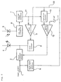
- Fig. 2 is a block diagram showing a construction of an optical transmitter according to an embodiment of the present invention.
- Back light of the optical output of laser 4 is monitored and converted into a current corresponding to the optical output by photodiode 5, and the current is converted into a voltage by current/voltage converter 6.
- the voltage is inputted to average value detector 7, by which average voltage 21 is produced.
- Output 21 of average value detector 7 is inputted to bias controller 9 which uses, as a reference voltage, output 22 of mark-space ratio detector 8 which detects an mark-space ratio value of input signal 1, and bias circuit 3 is controlled with an output of bias controller 9.
- Operation circuit 10 calculates a voltage value corresponding to output 21 of average value detector 7 and output 22 of mark-space ratio detector 8, and an output of operation circuit 10 is inputted to pulse current controller 12 together with reference voltage (Vref) 11, which controls pulse current driver 2.
- Vref reference voltage
- Operation circuit 10 of a control loop for pulse current which drives laser 4 calculates a peak value of the optical output from output 22 of mark-space ratio detector 8 which detects a mark-space ratio of input signal 1 and output 21 of average value detector 7.
- the peak value of the optical output is inputted to pulse current controller 12 which uses voltage Vref as reference voltage 11, and pulse current driver 2 is driven with an output of pulse current controller 12.
- the bias current of laser 4 is controlled with an output of bias circuit 3. Consequently, the optical output obtained has a fixed optical power and is free from a pulse width distortion irrespective of variation in characteristic of laser 4 as hereinafter described.
- Fig. 3 is a block diagram showing a construction of operation circuit 10 in the embodiment of the present invention described above.
- Operation circuit 10 includes first A/D converter 23 and second A/D converter 24 which receive output 21 of average value detector 7 and output 22 of mark ratio detector 8, respectively, and output X and Y of first A/D converter 23 and second A/D converter 24, respectively, to divider 25.
- laser 4 is driven by pulse current driver 2 and bias circuit 3, and converts input signal 1 into an optical signal. Part of the output of the optical signal is converted into a current by photodiode 5 and further converted into a voltage by current/voltage converter 6. The voltage is averaged by average value detector 7.
- Figs. 4(A), 4(B) and 4(C) are an example of time charts of the input electric signal, the output of current/voltage converter 6 and the output of average value detector 7 illustrated in Fig. 2, respectively.
- Input signal 1 illustrated in Fig. 4(A) is converted into an optical output by laser 4, and part of the optical output is converted into a current by photodiode 5 and further converted into a voltage by current/voltage converter 6.
- the output voltage of current/voltage converter 6 has such a waveform as seen from Fig. 4(B).
- the reason why the leading edge rising rate is delayed is that a peak value of the optical output cannot be detected due to a band limitation to a frequency characteristic of photodiode 5 which converts back light of the laser into current.
- the optical output average value illustrated in Fig. 4(C) is average voltage 21 of average value detector 7 and indicates an average value of the output of current/voltage converter 6 of Fig. 4(B).
- Figs. 5(A), 5(B) and 5(C) are diagrammatic views illustrating operation of operation circuit 10 in the case of mark-space ratio 1/2 or 1/4.
- the output of operation circuit 10 corresponds to a peak value of the optical output 21 and is inputted to pulse current controller 12, in which the peak value is compared with a reference voltage (Vref) 11, and amplified. Then pulse current driver 2 is operated with the output of pulse current controller 12.
- the optical output is controlled to the fixed level and the output of average value detector 7 is controlled so that the ratio thereof to the peak value of the optical output may be equal to the mark-space ratio detected by mark-space ratio detector 8.
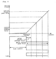
- Fig. 6 is a diagram illustrating an example of a driving current-optical output characteristic of the laser.
- the laser provides an optical output which is substantially in proportion to the driving current higher than the threshold current. Therefore, when the control described above is performed, the ratio between the pulse current average value and the pulse current peak value becomes substantially equal to the ratio between the optical output average value and the optical output peak value.
- the bias current of the laser is controlled so as to be substantially equal to the threshold current.
- Fig. 7 is a block diagram showing an internal construction of operation circuit 30 according to another embodiment of the present invention which corresponds to operation circuit 10 of Fig. 1.
- the present invention is advantageous in that it compensates for variations of the threshold current and the differential quantum efficiency caused by temperature variation or deterioration with the passage of time of a laser even upon high speed modulation of the laser thereby to allow production of an optical output having a fixed optical power and free from a pulse width distortion.
- the optical power is not limited by the frequency characteristic of a photodiode.
Landscapes
- Physics & Mathematics (AREA)
- Electromagnetism (AREA)
- Engineering & Computer Science (AREA)
- Computer Networks & Wireless Communication (AREA)
- Signal Processing (AREA)
- Optics & Photonics (AREA)
- Condensed Matter Physics & Semiconductors (AREA)
- General Physics & Mathematics (AREA)
- Semiconductor Lasers (AREA)
- Optical Communication System (AREA)
Applications Claiming Priority (2)
| Application Number | Priority Date | Filing Date | Title |
|---|---|---|---|
| JP804298 | 1998-01-19 | ||
| JP10008042A JP3085274B2 (ja) | 1998-01-19 | 1998-01-19 | 光送信器 |
Publications (3)
| Publication Number | Publication Date |
|---|---|
| EP0930678A2 true EP0930678A2 (fr) | 1999-07-21 |
| EP0930678A3 EP0930678A3 (fr) | 2001-01-17 |
| EP0930678B1 EP0930678B1 (fr) | 2004-09-29 |
Family
ID=11682301
Family Applications (1)
| Application Number | Title | Priority Date | Filing Date |
|---|---|---|---|
| EP99100367A Expired - Lifetime EP0930678B1 (fr) | 1998-01-19 | 1999-01-15 | Transmetteur optique |
Country Status (4)
| Country | Link |
|---|---|
| US (1) | US6192060B1 (fr) |
| EP (1) | EP0930678B1 (fr) |
| JP (1) | JP3085274B2 (fr) |
| DE (1) | DE69920540T2 (fr) |
Cited By (2)
| Publication number | Priority date | Publication date | Assignee | Title |
|---|---|---|---|---|
| EP1328048A3 (fr) * | 2001-12-20 | 2005-07-13 | Kabushiki Kaisha Toshiba | Dispositif de contrôle d'un élément émetteur de lumière, appareil à transmission optique, méthode et programme d'ordinateur pour déterminer le courant d'alimentation |
| WO2018186833A1 (fr) | 2017-04-04 | 2018-10-11 | Hewlett Packard Enterprise Development Lp | Réduction des tensions d'alimentation de dispositifs émetteurs optiques |
Families Citing this family (17)
| Publication number | Priority date | Publication date | Assignee | Title |
|---|---|---|---|---|
| JP3593646B2 (ja) * | 1999-03-19 | 2004-11-24 | 富士通株式会社 | バースト光送信回路 |
| JP3363133B2 (ja) * | 2000-07-21 | 2003-01-08 | 住友電気工業株式会社 | 波長多重分割伝送方法およびそのシステム |
| US20020027688A1 (en) * | 2000-09-05 | 2002-03-07 | Jim Stephenson | Fiber optic transceiver employing digital dual loop compensation |
| JPWO2002069464A1 (ja) * | 2001-02-23 | 2004-07-02 | 富士通株式会社 | 光送信器 |
| WO2002075403A1 (fr) | 2001-03-16 | 2002-09-26 | Photuris, Inc. | Procédé et dispositif d'égalisation du gain d'un signal optique dans un système de communication optique |
| US6947458B2 (en) * | 2001-06-07 | 2005-09-20 | Alcatel Communications, Inc. | Power control circuit for laser diode having wavelength compensation |
| US6826210B2 (en) * | 2001-06-07 | 2004-11-30 | Alcatel Communications, Inc. | Power control circuit for laser diode having wavelength compensation |
| US6917639B2 (en) * | 2001-08-09 | 2005-07-12 | Ricoh Company, Ltd. | Laser driver circuit |
| US7869477B2 (en) * | 2002-12-18 | 2011-01-11 | Lighttime, Llc | System and method for developing high output power nanosecond range pulses from continuous wave semiconductor laser systems |
| US8036539B2 (en) * | 2005-06-28 | 2011-10-11 | Finisar Corporation | Gigabit ethernet longwave optical transceiver module having amplified bias current |
| JP4570562B2 (ja) * | 2005-12-28 | 2010-10-27 | 古河電気工業株式会社 | 半導体レーザの駆動制御装置及び駆動制御方法 |
| US20090259217A1 (en) * | 2008-04-09 | 2009-10-15 | Searete Llc, A Limited Liability Corporation Of The State Of Delaware | Methods and systems associated with delivery of one or more agents to an individual |
| US20090259112A1 (en) * | 2008-04-09 | 2009-10-15 | Searete Llc, A Limited Liability Corporation Of The State Of Delaware | Sensors |
| US8971364B2 (en) * | 2011-01-19 | 2015-03-03 | Coherent, Inc. | Driving circuit for analog-modulated diode-laser |
| US8548336B2 (en) * | 2011-12-02 | 2013-10-01 | Semtech Corporation | Closed loop optical modulation amplitude control |
| CN106130657A (zh) * | 2016-06-17 | 2016-11-16 | 青岛海信宽带多媒体技术有限公司 | 一种光功率控制方法及装置 |
| CN116743260B (zh) * | 2023-08-15 | 2023-10-17 | 深圳市知用电子有限公司 | 激光信号传输系统 |
Family Cites Families (14)
| Publication number | Priority date | Publication date | Assignee | Title |
|---|---|---|---|---|
| US4355395A (en) * | 1978-04-10 | 1982-10-19 | British Telecommunications | Injection lasers |
| JP2503202B2 (ja) * | 1985-01-30 | 1996-06-05 | 株式会社リコー | 半導体レ−ザの出力制御装置 |
| US5127015A (en) * | 1990-04-17 | 1992-06-30 | Sharp Kabushiki Kaisha | Driving circuit of a semiconductor laser |
| US5177755A (en) * | 1991-05-31 | 1993-01-05 | Amoco Corporation | Laser feedback control circuit and method |
| JPH0563647A (ja) * | 1991-08-30 | 1993-03-12 | Furukawa Electric Co Ltd:The | 光送信装置 |
| JPH0590673A (ja) | 1991-09-27 | 1993-04-09 | Mitsubishi Electric Corp | 光送信器 |
| US5268916A (en) * | 1992-06-15 | 1993-12-07 | Alcatel Network Systems, Inc. | Laser bias and modulation circuit |
| JP2630199B2 (ja) * | 1993-05-07 | 1997-07-16 | 日本電気株式会社 | 光増幅器警報回路 |
| DE4316811A1 (de) * | 1993-05-19 | 1994-11-24 | Philips Patentverwaltung | Optisches Übertragungssystem mit einer Laserdiode |
| GB2281163A (en) * | 1993-08-04 | 1995-02-22 | Fulcrum Communications Limited | Optical transmitters |
| US5448629A (en) * | 1993-10-14 | 1995-09-05 | At&T Corp. | Amplitude detection scheme for optical transmitter control |
| JPH088831A (ja) * | 1994-06-22 | 1996-01-12 | Fujitsu Ltd | 光送信機 |
| US5812572A (en) * | 1996-07-01 | 1998-09-22 | Pacific Fiberoptics, Inc. | Intelligent fiberoptic transmitters and methods of operating and manufacturing the same |
| JP3700296B2 (ja) * | 1996-11-29 | 2005-09-28 | 富士ゼロックス株式会社 | 半導体レーザ駆動装置および画像記録装置 |
-
1998
- 1998-01-19 JP JP10008042A patent/JP3085274B2/ja not_active Expired - Lifetime
-
1999
- 1999-01-15 US US09/231,648 patent/US6192060B1/en not_active Expired - Fee Related
- 1999-01-15 EP EP99100367A patent/EP0930678B1/fr not_active Expired - Lifetime
- 1999-01-15 DE DE69920540T patent/DE69920540T2/de not_active Expired - Fee Related
Cited By (3)
| Publication number | Priority date | Publication date | Assignee | Title |
|---|---|---|---|---|
| EP1328048A3 (fr) * | 2001-12-20 | 2005-07-13 | Kabushiki Kaisha Toshiba | Dispositif de contrôle d'un élément émetteur de lumière, appareil à transmission optique, méthode et programme d'ordinateur pour déterminer le courant d'alimentation |
| WO2018186833A1 (fr) | 2017-04-04 | 2018-10-11 | Hewlett Packard Enterprise Development Lp | Réduction des tensions d'alimentation de dispositifs émetteurs optiques |
| EP3607675A4 (fr) * | 2017-04-04 | 2020-12-02 | Hewlett-Packard Enterprise Development LP | Réduction des tensions d'alimentation de dispositifs émetteurs optiques |
Also Published As
| Publication number | Publication date |
|---|---|
| EP0930678B1 (fr) | 2004-09-29 |
| JP3085274B2 (ja) | 2000-09-04 |
| DE69920540D1 (de) | 2004-11-04 |
| JPH11205248A (ja) | 1999-07-30 |
| US6192060B1 (en) | 2001-02-20 |
| EP0930678A3 (fr) | 2001-01-17 |
| DE69920540T2 (de) | 2005-03-03 |
Similar Documents
| Publication | Publication Date | Title |
|---|---|---|
| US6192060B1 (en) | Optical transmitter | |
| EP0539038A2 (fr) | Emetteurs optiques | |
| US5570227A (en) | Method and apparatus for preventing occurrence of surge light in optical amplifier/transmitter apparatus | |
| US7020169B2 (en) | Laser diode driver with extinction ratio control | |
| US6982689B2 (en) | Light-emitting element drive apparatus | |
| US5187713A (en) | Nonlinear device control methods and apparatus | |
| US7809034B2 (en) | Auto-power control circuit to maintain extinction ratio of optical output from laser diode | |
| JPH06103765B2 (ja) | 半導体レーザバイアス電流制御方式 | |
| US7512166B2 (en) | Apparatus and method for controlling optical power and extinction ratio | |
| JPH0814501B2 (ja) | 光給電型信号処理装置 | |
| JP2005057216A (ja) | レーザダイオード駆動回路及び光送信装置 | |
| JPH09283848A (ja) | レーザダイオード駆動回路 | |
| JPH0553078B2 (fr) | ||
| JPH04304689A (ja) | 光送信器 | |
| JPH0590673A (ja) | 光送信器 | |
| JPH06244800A (ja) | 光送信器 | |
| JPS589445A (ja) | 光伝送方式 | |
| JP2626470B2 (ja) | デジタル光通信における光出力制御装置 | |
| JPH06181351A (ja) | レーザダイオード駆動回路 | |
| JPH0313133A (ja) | 光送信装置 | |
| JP2004056830A (ja) | バースト信号消光比制御回路及びその集積回路、バースト信号消光比制御方法、コンピュータプログラム並びにレーザダイオード駆動回路 | |
| JPH02240627A (ja) | 光変調制御方式 | |
| JPH03209890A (ja) | 発光素子の自動光出力制御方法とその制御回路 | |
| JPH10190575A (ja) | 自動光出力制御回路 | |
| JPH0716173B2 (ja) | 光受信回路 |
Legal Events
| Date | Code | Title | Description |
|---|---|---|---|
| PUAI | Public reference made under article 153(3) epc to a published international application that has entered the european phase |
Free format text: ORIGINAL CODE: 0009012 |
|
| AK | Designated contracting states |
Kind code of ref document: A2 Designated state(s): DE FR GB |
|
| AX | Request for extension of the european patent |
Free format text: AL;LT;LV;MK;RO;SI |
|
| PUAL | Search report despatched |
Free format text: ORIGINAL CODE: 0009013 |
|
| AK | Designated contracting states |
Kind code of ref document: A3 Designated state(s): AT BE CH CY DE DK ES FI FR GB GR IE IT LI LU MC NL PT SE |
|
| AX | Request for extension of the european patent |
Free format text: AL;LT;LV;MK;RO;SI |
|
| RIC1 | Information provided on ipc code assigned before grant |
Free format text: 7H 01S 3/13 A, 7H 04B 10/04 B |
|
| 17P | Request for examination filed |
Effective date: 20001209 |
|
| AKX | Designation fees paid |
Free format text: DE FR GB |
|
| GRAP | Despatch of communication of intention to grant a patent |
Free format text: ORIGINAL CODE: EPIDOSNIGR1 |
|
| RIC1 | Information provided on ipc code assigned before grant |
Ipc: 7H 01S 5/068 B Ipc: 7H 04B 10/04 B Ipc: 7H 01S 3/13 A |
|
| GRAS | Grant fee paid |
Free format text: ORIGINAL CODE: EPIDOSNIGR3 |
|
| GRAA | (expected) grant |
Free format text: ORIGINAL CODE: 0009210 |
|
| AK | Designated contracting states |
Kind code of ref document: B1 Designated state(s): DE FR GB |
|
| REG | Reference to a national code |
Ref country code: GB Ref legal event code: FG4D |
|
| REF | Corresponds to: |
Ref document number: 69920540 Country of ref document: DE Date of ref document: 20041104 Kind code of ref document: P |
|
| PLBE | No opposition filed within time limit |
Free format text: ORIGINAL CODE: 0009261 |
|
| STAA | Information on the status of an ep patent application or granted ep patent |
Free format text: STATUS: NO OPPOSITION FILED WITHIN TIME LIMIT |
|
| ET | Fr: translation filed | ||
| 26N | No opposition filed |
Effective date: 20050630 |
|
| PGFP | Annual fee paid to national office [announced via postgrant information from national office to epo] |
Ref country code: DE Payment date: 20090108 Year of fee payment: 11 |
|
| PGFP | Annual fee paid to national office [announced via postgrant information from national office to epo] |
Ref country code: GB Payment date: 20090114 Year of fee payment: 11 |
|
| PGFP | Annual fee paid to national office [announced via postgrant information from national office to epo] |
Ref country code: FR Payment date: 20090113 Year of fee payment: 11 |
|
| GBPC | Gb: european patent ceased through non-payment of renewal fee |
Effective date: 20100115 |
|
| REG | Reference to a national code |
Ref country code: FR Ref legal event code: ST Effective date: 20100930 |
|
| PG25 | Lapsed in a contracting state [announced via postgrant information from national office to epo] |
Ref country code: FR Free format text: LAPSE BECAUSE OF NON-PAYMENT OF DUE FEES Effective date: 20100201 |
|
| PG25 | Lapsed in a contracting state [announced via postgrant information from national office to epo] |
Ref country code: DE Free format text: LAPSE BECAUSE OF NON-PAYMENT OF DUE FEES Effective date: 20100803 |
|
| PG25 | Lapsed in a contracting state [announced via postgrant information from national office to epo] |
Ref country code: GB Free format text: LAPSE BECAUSE OF NON-PAYMENT OF DUE FEES Effective date: 20100115 |