EP0932192A1 - Ätzen einer Platinelektrode - Google Patents
Ätzen einer Platinelektrode Download PDFInfo
- Publication number
- EP0932192A1 EP0932192A1 EP99106072A EP99106072A EP0932192A1 EP 0932192 A1 EP0932192 A1 EP 0932192A1 EP 99106072 A EP99106072 A EP 99106072A EP 99106072 A EP99106072 A EP 99106072A EP 0932192 A1 EP0932192 A1 EP 0932192A1
- Authority
- EP
- European Patent Office
- Prior art keywords
- etching
- electrode film
- platinum
- film
- dry
- Prior art date
- Legal status (The legal status is an assumption and is not a legal conclusion. Google has not performed a legal analysis and makes no representation as to the accuracy of the status listed.)
- Granted
Links
Images

Classifications
-
- H—ELECTRICITY
- H10—SEMICONDUCTOR DEVICES; ELECTRIC SOLID-STATE DEVICES NOT OTHERWISE PROVIDED FOR
- H10P—GENERIC PROCESSES OR APPARATUS FOR THE MANUFACTURE OR TREATMENT OF DEVICES COVERED BY CLASS H10
- H10P70/00—Cleaning of wafers, substrates or parts of devices
- H10P70/20—Cleaning during device manufacture
- H10P70/27—Cleaning during device manufacture during, before or after processing of conductive materials, e.g. polysilicon or amorphous silicon layers
- H10P70/273—Cleaning during device manufacture during, before or after processing of conductive materials, e.g. polysilicon or amorphous silicon layers the processing being a delineation of conductive layers, e.g. by RIE
-
- H—ELECTRICITY
- H10—SEMICONDUCTOR DEVICES; ELECTRIC SOLID-STATE DEVICES NOT OTHERWISE PROVIDED FOR
- H10D—INORGANIC ELECTRIC SEMICONDUCTOR DEVICES
- H10D1/00—Resistors, capacitors or inductors
- H10D1/60—Capacitors
- H10D1/68—Capacitors having no potential barriers
- H10D1/692—Electrodes
-
- H—ELECTRICITY
- H10—SEMICONDUCTOR DEVICES; ELECTRIC SOLID-STATE DEVICES NOT OTHERWISE PROVIDED FOR
- H10D—INORGANIC ELECTRIC SEMICONDUCTOR DEVICES
- H10D1/00—Resistors, capacitors or inductors
- H10D1/60—Capacitors
- H10D1/68—Capacitors having no potential barriers
- H10D1/692—Electrodes
- H10D1/694—Electrodes comprising noble metals or noble metal oxides
-
- H—ELECTRICITY
- H10—SEMICONDUCTOR DEVICES; ELECTRIC SOLID-STATE DEVICES NOT OTHERWISE PROVIDED FOR
- H10P—GENERIC PROCESSES OR APPARATUS FOR THE MANUFACTURE OR TREATMENT OF DEVICES COVERED BY CLASS H10
- H10P50/00—Etching of wafers, substrates or parts of devices
- H10P50/20—Dry etching; Plasma etching; Reactive-ion etching
- H10P50/26—Dry etching; Plasma etching; Reactive-ion etching of conductive or resistive materials
- H10P50/264—Dry etching; Plasma etching; Reactive-ion etching of conductive or resistive materials by chemical means
- H10P50/266—Dry etching; Plasma etching; Reactive-ion etching of conductive or resistive materials by chemical means by vapour etching only
- H10P50/267—Dry etching; Plasma etching; Reactive-ion etching of conductive or resistive materials by chemical means by vapour etching only using plasmas
Definitions
- the present invention relates to a method of manufacturing a semiconductor device having a capacitor using a high permittivity dielectric film or a ferroelectric film as a capacitor dielectric film, and in particular, to a method including a step of dry etching of the capacitor dielectric film.
- FIG. 3(a), Fig. 3(b), Fig. 3(c), and Fig. 3(d) are sectional views for explaining the method of forming a capacitor included in a conventional semiconductor device.
- a platinum bottom electrode film 1 a dielectric film 2 comprised of a high permittivity dielectric film or a ferroelectric film, and a platinum top electrode film 3 are formed on a substrate 4 on which a silicon oxide film is deposited. Then, using a photoresist film 5 as mask, the platinum top electrode film 3 and the dielectric film 2 are dry-etched by using etching gas containing chlorine, and processed into a shape as shown in Fig. 3(b). Finally, by dry-etching the platinum bottom electrode film 1, a capacitor is formed.
- a defect 8 may be formed in a side wall 6 of the dielectric film 2 as shown in Fig. 3(c), or the side wall 6 is often degenerated into a difference substance 9 from the dielectric. When such state appears, short circuit of capacitor or increase of leakage current occurs, and the function as the capacitor is lost in an extreme case.
- the cause of appearance of such phenomenon may be considered as follows. On the side walls 6 of the platinum top electrode film 3 and the dielectric film 2 which are dry-etched, and on the surface 7 of the platinum bottom electrode film 1 which is exposed, atoms, ions or radicals of chlorine generated by decomposition of the etching gas due to discharge are massively deposited. These chlorine atoms, ions or radicals easily react with moisture to form an acidic aqueous solution, that is, hydrochloric acid.
- the side wall 6 of the dielectric film 2 composed of a dielectric oxide violently reacts with this hydrochloric acid, and the dielectric film 2 is eroded, or degenerated into other substance 9 different from the dielectric. As a result, it is considered to lead to short circuit of capacitor, increase of leakage current, or loss of function as capacitor.
- An object of the present invention is to provide a method of manufacturing a semiconductor device capable of preventing erosion of dielectric film, and suppressing occurrence of short circuit of capacitor and increase of leakage current.
- a method of manufacturing a semiconductor device comprises a step of forming a platinum bottom electrode film, a dielectric film, and a platinum top electrode film on a substrate on which circuit elements and wiring are formed, a step of dry-etching selectively the platinum top electrode film and the dielectric film by using etching gas containing at least one of chlorine, bromine and iodine, a step of heating the substrate after the step of dry-etching, and a step of etching the platinum bottom electrode film.
- decomposition products of the etching gas containing chlorine, bromine or iodine depositing on the side wall of the dielectric film or on the surface of the platinum bottom electrode film at the time of dry-etching are extremely decreased. It hence suppresses occurrence of defect or degeneration of the dielectric film which is induced by reacting the dielectric film with the acid formed by reaction of these decomposition products with moisture dielectric. Therefore occurrence of short circuit in capacitor and increase of leakage current may be extremely suppressed.
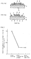
- a platinum bottom electrode film 1 a dielectric film 2 composed of a high permittivity dielectric material or a ferroelectric material, and a platinum top electrode film 3 are formed on a substrate 4 on which circuit elements, wiring and an insulating film are formed.
- heating atmosphere aside from the nitrogen gas, argon gas, helium gas or other inert gas may be used, or it may be also done in vacuum.
- the reason of effect caused by heating is estimated as follows from the results of measurement of residual chlorine concentration shown in Fig. 2.
- the residual chlorine concentration after heating process shown in Fig. 2 corresponds to the case of heating conditions shown in the second embodiment.
- the residual chlorine concentration after heating process is decreased to about one-third as compared with the residual chlorine concentration right after dry-etching.
- etching gas containing chlorine is used as etching gas, but the same effects as in the embodiment are obtained by using etching gas containing bromine or iodine, instead of chlorine, or etching gas containing two or more of chlorine, bromine and iodine.
Landscapes
- Drying Of Semiconductors (AREA)
- Semiconductor Memories (AREA)
- Semiconductor Integrated Circuits (AREA)
Applications Claiming Priority (3)
| Application Number | Priority Date | Filing Date | Title |
|---|---|---|---|
| JP1682995 | 1995-02-03 | ||
| JP7016829A JP2953974B2 (ja) | 1995-02-03 | 1995-02-03 | 半導体装置の製造方法 |
| EP96101154A EP0725430B1 (de) | 1995-02-03 | 1996-01-27 | Verfahren zur Herstellung einer Halbleiteranordnung mit einem Kondensator |
Related Parent Applications (1)
| Application Number | Title | Priority Date | Filing Date |
|---|---|---|---|
| EP96101154A Division EP0725430B1 (de) | 1995-02-03 | 1996-01-27 | Verfahren zur Herstellung einer Halbleiteranordnung mit einem Kondensator |
Publications (2)
| Publication Number | Publication Date |
|---|---|
| EP0932192A1 true EP0932192A1 (de) | 1999-07-28 |
| EP0932192B1 EP0932192B1 (de) | 2003-06-11 |
Family
ID=11927088
Family Applications (2)
| Application Number | Title | Priority Date | Filing Date |
|---|---|---|---|
| EP96101154A Expired - Lifetime EP0725430B1 (de) | 1995-02-03 | 1996-01-27 | Verfahren zur Herstellung einer Halbleiteranordnung mit einem Kondensator |
| EP99106072A Expired - Lifetime EP0932192B1 (de) | 1995-02-03 | 1996-01-27 | Ätzen einer Platinelektrode und eine dielektrische oder ferroelektrische Schicht |
Family Applications Before (1)
| Application Number | Title | Priority Date | Filing Date |
|---|---|---|---|
| EP96101154A Expired - Lifetime EP0725430B1 (de) | 1995-02-03 | 1996-01-27 | Verfahren zur Herstellung einer Halbleiteranordnung mit einem Kondensator |
Country Status (6)
| Country | Link |
|---|---|
| US (1) | US5652171A (de) |
| EP (2) | EP0725430B1 (de) |
| JP (1) | JP2953974B2 (de) |
| KR (1) | KR0185489B1 (de) |
| CN (1) | CN1080926C (de) |
| DE (2) | DE69628677T2 (de) |
Cited By (1)
| Publication number | Priority date | Publication date | Assignee | Title |
|---|---|---|---|---|
| WO2002052631A2 (en) | 2000-12-21 | 2002-07-04 | Infineon Technologies North America Corp. | An isotropic etch to form mim capacitor top plates |
Families Citing this family (34)
| Publication number | Priority date | Publication date | Assignee | Title |
|---|---|---|---|---|
| JPH09251983A (ja) * | 1996-03-15 | 1997-09-22 | Rohm Co Ltd | ドライエッチング方法 |
| DE19646208C2 (de) * | 1996-11-08 | 2001-08-30 | Infineon Technologies Ag | Verfahren zur Herstellung eines Kondensators und Speicherfeld |
| KR19980060614A (ko) * | 1996-12-31 | 1998-10-07 | 김영환 | 반도체 소자의 제조방법 |
| JP3024747B2 (ja) * | 1997-03-05 | 2000-03-21 | 日本電気株式会社 | 半導体メモリの製造方法 |
| EP0865079A3 (de) | 1997-03-13 | 1999-10-20 | Applied Materials, Inc. | Verfahren zur Beseitigung von auf geätzten Platinflächen abgelagerten Verunreinigungen |
| DE19712540C1 (de) * | 1997-03-25 | 1998-08-13 | Siemens Ag | Herstellverfahren für eine Kondensatorelektrode aus einem Platinmetall |
| US5846884A (en) * | 1997-06-20 | 1998-12-08 | Siemens Aktiengesellschaft | Methods for metal etching with reduced sidewall build up during integrated circuit manufacturing |
| KR100458293B1 (ko) * | 1997-12-20 | 2005-02-05 | 주식회사 하이닉스반도체 | 반도체소자의금속배선후처리방법 |
| US6323132B1 (en) | 1998-01-13 | 2001-11-27 | Applied Materials, Inc. | Etching methods for anisotropic platinum profile |
| US6265318B1 (en) | 1998-01-13 | 2001-07-24 | Applied Materials, Inc. | Iridium etchant methods for anisotropic profile |
| US6919168B2 (en) | 1998-01-13 | 2005-07-19 | Applied Materials, Inc. | Masking methods and etching sequences for patterning electrodes of high density RAM capacitors |
| JP2002510146A (ja) | 1998-01-13 | 2002-04-02 | アプライド マテリアルズ インコーポレイテッド | 異方性プラチナプロファイルのエッチング方法 |
| KR100333127B1 (ko) * | 1998-06-29 | 2002-09-05 | 주식회사 하이닉스반도체 | 반도체소자의캐패시터제조방법 |
| US6323081B1 (en) | 1998-09-03 | 2001-11-27 | Micron Technology, Inc. | Diffusion barrier layers and methods of forming same |
| US6204172B1 (en) | 1998-09-03 | 2001-03-20 | Micron Technology, Inc. | Low temperature deposition of barrier layers |
| US7060584B1 (en) * | 1999-07-12 | 2006-06-13 | Zilog, Inc. | Process to improve high performance capacitor properties in integrated MOS technology |
| US6458648B1 (en) * | 1999-12-17 | 2002-10-01 | Agere Systems Guardian Corp. | Method for in-situ removal of side walls in MOM capacitor formation |
| KR100358149B1 (ko) * | 2000-06-30 | 2002-10-25 | 주식회사 하이닉스반도체 | 플라즈마 처리를 이용하여 강유전체 캐패시터의 열화를회복시키는 강유전체 메모리 소자 제조 방법 |
| US6444479B1 (en) * | 2001-04-18 | 2002-09-03 | Hynix Semiconductor Inc. | Method for forming capacitor of semiconductor device |
| JP4032916B2 (ja) * | 2001-11-28 | 2008-01-16 | 三菱化学株式会社 | エッチング液 |
| EP1321977A1 (de) * | 2001-12-17 | 2003-06-25 | AMI Semiconductor Belgium BVBA | Verfahren zur Reduzierung von elektrischen Ladungen erzeugt durch einen vorherigen Prozessschritt auf einer leitenden Struktur |
| JP2003257942A (ja) * | 2002-02-28 | 2003-09-12 | Fujitsu Ltd | 半導体装置の製造方法 |
| JP4865978B2 (ja) * | 2002-02-28 | 2012-02-01 | 富士通セミコンダクター株式会社 | 半導体装置の製造方法 |
| TWI304230B (en) * | 2003-05-30 | 2008-12-11 | Tokyo Electron Ltd | Method and system for etching a high-k dielectric material |
| JP4085094B2 (ja) * | 2004-02-19 | 2008-04-30 | シャープ株式会社 | 導電素子基板の製造方法、液晶表示装置の製造方法 |
| US7071117B2 (en) * | 2004-02-27 | 2006-07-04 | Micron Technology, Inc. | Semiconductor devices and methods for depositing a dielectric film |
| JP2006313833A (ja) * | 2005-05-09 | 2006-11-16 | Seiko Epson Corp | 強誘電体キャパシタの形成方法、強誘電体キャパシタおよび電子デバイス |
| US20060278339A1 (en) * | 2005-06-13 | 2006-12-14 | Lam Research Corporation, A Delaware Corporation | Etch rate uniformity using the independent movement of electrode pieces |
| JP2009266952A (ja) * | 2008-04-23 | 2009-11-12 | Seiko Epson Corp | デバイスの製造方法及び製造装置 |
| JP2011119779A (ja) * | 2011-03-22 | 2011-06-16 | Seiko Epson Corp | 強誘電体キャパシタの形成方法、強誘電体キャパシタおよび電子デバイス |
| CN102956430A (zh) * | 2012-05-25 | 2013-03-06 | 深圳市华星光电技术有限公司 | 取代膜层上氯原子的方法 |
| US9224592B2 (en) * | 2013-09-12 | 2015-12-29 | Texas Intruments Incorporated | Method of etching ferroelectric capacitor stack |
| JP6210039B2 (ja) * | 2014-09-24 | 2017-10-11 | セントラル硝子株式会社 | 付着物の除去方法及びドライエッチング方法 |
| JP7199174B2 (ja) * | 2018-07-26 | 2023-01-05 | 東京エレクトロン株式会社 | エッチング方法 |
Citations (1)
| Publication number | Priority date | Publication date | Assignee | Title |
|---|---|---|---|---|
| JPS61160939A (ja) * | 1985-01-09 | 1986-07-21 | Nec Corp | ドライエツチング後Si表面損傷の乾式による除去方法 |
Family Cites Families (14)
| Publication number | Priority date | Publication date | Assignee | Title |
|---|---|---|---|---|
| US4325984B2 (en) * | 1980-07-28 | 1998-03-03 | Fairchild Camera & Inst | Plasma passivation technique for the prevention of post-etch corrosion of plasma-etched aluminum films |
| JPS593927A (ja) * | 1982-06-29 | 1984-01-10 | Fujitsu Ltd | 薄膜のエツチング方法 |
| JPS59189633A (ja) * | 1983-04-13 | 1984-10-27 | Fujitsu Ltd | 半導体装置の製造方法 |
| US4666555A (en) * | 1985-08-23 | 1987-05-19 | Intel Corporation | Plasma etching of silicon using fluorinated gas mixtures |
| US4847212A (en) * | 1987-01-12 | 1989-07-11 | Itt Gallium Arsenide Technology Center | Self-aligned gate FET process using undercut etch mask |
| JPH02151031A (ja) * | 1988-12-02 | 1990-06-11 | Hitachi Ltd | 半導体装置の製造方法 |
| JPH03155621A (ja) * | 1989-07-12 | 1991-07-03 | Toshiba Corp | ドライエッチング方法 |
| US5316572A (en) * | 1989-12-11 | 1994-05-31 | Nmb Ltd. | Method of manufacturing concrete for placement in air not requiring consolidation |
| WO1992000601A1 (fr) * | 1990-06-27 | 1992-01-09 | Fujitsu Limited | Procede de fabrication d'un circuit integre a semi-conducteurs et appareil de fabrication correspondant |
| JPH0467636A (ja) * | 1990-07-06 | 1992-03-03 | Mitsubishi Electric Corp | 半導体装置の製造方法 |
| US5216572A (en) * | 1992-03-19 | 1993-06-01 | Ramtron International Corporation | Structure and method for increasing the dielectric constant of integrated ferroelectric capacitors |
| JPH0649667A (ja) * | 1992-07-30 | 1994-02-22 | Sharp Corp | ドライエッチング方法及びその装置 |
| US5335138A (en) * | 1993-02-12 | 1994-08-02 | Micron Semiconductor, Inc. | High dielectric constant capacitor and method of manufacture |
| JP3460347B2 (ja) * | 1994-03-30 | 2003-10-27 | 松下電器産業株式会社 | 半導体装置の製造方法 |
-
1995
- 1995-02-03 JP JP7016829A patent/JP2953974B2/ja not_active Expired - Fee Related
-
1996
- 1996-01-27 DE DE69628677T patent/DE69628677T2/de not_active Expired - Lifetime
- 1996-01-27 DE DE69613723T patent/DE69613723T2/de not_active Expired - Lifetime
- 1996-01-27 EP EP96101154A patent/EP0725430B1/de not_active Expired - Lifetime
- 1996-01-27 EP EP99106072A patent/EP0932192B1/de not_active Expired - Lifetime
- 1996-01-31 US US08/594,945 patent/US5652171A/en not_active Expired - Lifetime
- 1996-02-02 KR KR1019960002513A patent/KR0185489B1/ko not_active Expired - Fee Related
- 1996-02-02 CN CN96101296A patent/CN1080926C/zh not_active Expired - Fee Related
Patent Citations (1)
| Publication number | Priority date | Publication date | Assignee | Title |
|---|---|---|---|---|
| JPS61160939A (ja) * | 1985-01-09 | 1986-07-21 | Nec Corp | ドライエツチング後Si表面損傷の乾式による除去方法 |
Non-Patent Citations (1)
| Title |
|---|
| PATENT ABSTRACTS OF JAPAN vol. 010, no. 363 (E - 461) 5 December 1986 (1986-12-05) * |
Cited By (2)
| Publication number | Priority date | Publication date | Assignee | Title |
|---|---|---|---|---|
| WO2002052631A2 (en) | 2000-12-21 | 2002-07-04 | Infineon Technologies North America Corp. | An isotropic etch to form mim capacitor top plates |
| WO2002052631A3 (en) * | 2000-12-21 | 2003-12-24 | Infineon Technologies Corp | An isotropic etch to form mim capacitor top plates |
Also Published As
| Publication number | Publication date |
|---|---|
| CN1080926C (zh) | 2002-03-13 |
| CN1136218A (zh) | 1996-11-20 |
| EP0725430B1 (de) | 2001-07-11 |
| KR0185489B1 (ko) | 1999-04-15 |
| JPH08213364A (ja) | 1996-08-20 |
| DE69628677D1 (de) | 2003-07-17 |
| EP0725430A2 (de) | 1996-08-07 |
| DE69613723T2 (de) | 2002-04-25 |
| EP0725430A3 (de) | 1998-05-27 |
| DE69613723D1 (de) | 2001-08-16 |
| US5652171A (en) | 1997-07-29 |
| DE69628677T2 (de) | 2004-05-13 |
| JP2953974B2 (ja) | 1999-09-27 |
| EP0932192B1 (de) | 2003-06-11 |
Similar Documents
| Publication | Publication Date | Title |
|---|---|---|
| EP0932192B1 (de) | Ätzen einer Platinelektrode und eine dielektrische oder ferroelektrische Schicht | |
| US5685951A (en) | Methods and etchants for etching oxides of silicon with low selectivity in a vapor phase system | |
| US6254792B1 (en) | Isotropic dry cleaning process for noble metal integrated circuit structures | |
| KR100230908B1 (ko) | 반도체 장치의 제조 방법 | |
| KR940000913B1 (ko) | 플라즈마 에칭에 관한 원상태 포토레지스트의 캡핑방법 | |
| US5256245A (en) | Use of a clean up step to form more vertical profiles of polycrystalline silicon sidewalls during the manufacture of a semiconductor device | |
| US5624583A (en) | Method of manufacturing semiconductor device | |
| KR100269323B1 (ko) | 반도체장치의백금막식각방법 | |
| US5685950A (en) | Dry etching method | |
| JP3067737B2 (ja) | 酸化バナジウム膜のプラズマエッチング方法 | |
| US20030047532A1 (en) | Method of etching ferroelectric layers | |
| US6544896B1 (en) | Method for enhancing etching of TiSix | |
| US6528429B2 (en) | Methods of etching insulative materials, of forming electrical devices, and of forming capacitors | |
| JPH03241829A (ja) | 半導体装置の製造方法 | |
| US20010054599A1 (en) | Etching method | |
| US7078160B2 (en) | Selective surface exposure, cleans, and conditioning of the germanium film in a Ge photodetector | |
| KR100378345B1 (ko) | 백금 박막의 건식 식각 방법 | |
| JP3081200B2 (ja) | 電子デバイスの製造方法 | |
| JP2569754B2 (ja) | 化合物半導体装置の製造方法 | |
| JP3440599B2 (ja) | ビアホール形成方法 | |
| KR20010112086A (ko) | 반도체 장치의 제조 방법 | |
| US6184149B1 (en) | Method for monitoring self-aligned contact etching | |
| JPH07106298A (ja) | 半導体基板の処理方法 | |
| JPH0963988A (ja) | 高融点金属含有膜のエッチング方法並びにそれを用いた半導体装置およびその製造方法 | |
| JPH11340214A (ja) | 半導体装置の製造方法 |
Legal Events
| Date | Code | Title | Description |
|---|---|---|---|
| PUAI | Public reference made under article 153(3) epc to a published international application that has entered the european phase |
Free format text: ORIGINAL CODE: 0009012 |
|
| AC | Divisional application: reference to earlier application |
Ref document number: 725430 Country of ref document: EP |
|
| AK | Designated contracting states |
Kind code of ref document: A1 Designated state(s): DE FR GB NL |
|
| 17P | Request for examination filed |
Effective date: 19991021 |
|
| RAP1 | Party data changed (applicant data changed or rights of an application transferred) |
Owner name: MATSUSHITA ELECTRIC INDUSTRIAL CO., LTD. |
|
| GRAH | Despatch of communication of intention to grant a patent |
Free format text: ORIGINAL CODE: EPIDOS IGRA |
|
| RTI1 | Title (correction) |
Free format text: ETCHING OF A PLATINUM ELECTRODE AND A DIELECTRIC OR FERROELECTRIC LAYER |
|
| GRAH | Despatch of communication of intention to grant a patent |
Free format text: ORIGINAL CODE: EPIDOS IGRA |
|
| GRAA | (expected) grant |
Free format text: ORIGINAL CODE: 0009210 |
|
| AC | Divisional application: reference to earlier application |
Ref document number: 0725430 Country of ref document: EP Kind code of ref document: P |
|
| AK | Designated contracting states |
Designated state(s): DE FR GB NL |
|
| REG | Reference to a national code |
Ref country code: GB Ref legal event code: FG4D |
|
| REF | Corresponds to: |
Ref document number: 69628677 Country of ref document: DE Date of ref document: 20030717 Kind code of ref document: P |
|
| ET | Fr: translation filed | ||
| PLBE | No opposition filed within time limit |
Free format text: ORIGINAL CODE: 0009261 |
|
| STAA | Information on the status of an ep patent application or granted ep patent |
Free format text: STATUS: NO OPPOSITION FILED WITHIN TIME LIMIT |
|
| 26N | No opposition filed |
Effective date: 20040312 |
|
| REG | Reference to a national code |
Ref country code: GB Ref legal event code: 746 Effective date: 20091221 |
|
| REG | Reference to a national code |
Ref country code: NL Ref legal event code: V1 Effective date: 20110801 |
|
| PG25 | Lapsed in a contracting state [announced via postgrant information from national office to epo] |
Ref country code: NL Free format text: LAPSE BECAUSE OF NON-PAYMENT OF DUE FEES Effective date: 20110801 |
|
| PGFP | Annual fee paid to national office [announced via postgrant information from national office to epo] |
Ref country code: FR Payment date: 20120202 Year of fee payment: 17 |
|
| PGFP | Annual fee paid to national office [announced via postgrant information from national office to epo] |
Ref country code: DE Payment date: 20120125 Year of fee payment: 17 |
|
| PGFP | Annual fee paid to national office [announced via postgrant information from national office to epo] |
Ref country code: GB Payment date: 20120125 Year of fee payment: 17 |
|
| GBPC | Gb: european patent ceased through non-payment of renewal fee |
Effective date: 20130127 |
|
| REG | Reference to a national code |
Ref country code: FR Ref legal event code: ST Effective date: 20130930 |
|
| PG25 | Lapsed in a contracting state [announced via postgrant information from national office to epo] |
Ref country code: DE Free format text: LAPSE BECAUSE OF NON-PAYMENT OF DUE FEES Effective date: 20130801 |
|
| REG | Reference to a national code |
Ref country code: DE Ref legal event code: R119 Ref document number: 69628677 Country of ref document: DE Effective date: 20130801 |
|
| PG25 | Lapsed in a contracting state [announced via postgrant information from national office to epo] |
Ref country code: GB Free format text: LAPSE BECAUSE OF NON-PAYMENT OF DUE FEES Effective date: 20130127 Ref country code: FR Free format text: LAPSE BECAUSE OF NON-PAYMENT OF DUE FEES Effective date: 20130131 |
|
| PGFP | Annual fee paid to national office [announced via postgrant information from national office to epo] |
Ref country code: NL Payment date: 20100131 Year of fee payment: 15 |