EP0936785A2 - Verschiebungsausgleich für parallele Übertragung - Google Patents
Verschiebungsausgleich für parallele Übertragung Download PDFInfo
- Publication number
- EP0936785A2 EP0936785A2 EP99400357A EP99400357A EP0936785A2 EP 0936785 A2 EP0936785 A2 EP 0936785A2 EP 99400357 A EP99400357 A EP 99400357A EP 99400357 A EP99400357 A EP 99400357A EP 0936785 A2 EP0936785 A2 EP 0936785A2
- Authority
- EP
- European Patent Office
- Prior art keywords
- channel
- data
- frame
- section
- circuit
- Prior art date
- Legal status (The legal status is an assumption and is not a legal conclusion. Google has not performed a legal analysis and makes no representation as to the accuracy of the status listed.)
- Withdrawn
Links
Images









Classifications
-
- H—ELECTRICITY
- H04—ELECTRIC COMMUNICATION TECHNIQUE
- H04L—TRANSMISSION OF DIGITAL INFORMATION, e.g. TELEGRAPHIC COMMUNICATION
- H04L25/00—Baseband systems
- H04L25/02—Details ; arrangements for supplying electrical power along data transmission lines
- H04L25/14—Channel dividing arrangements, i.e. in which a single bit stream is divided between several baseband channels and reassembled at the receiver
-
- H—ELECTRICITY
- H03—ELECTRONIC CIRCUITRY
- H03M—CODING; DECODING; CODE CONVERSION IN GENERAL
- H03M7/00—Conversion of a code where information is represented by a given sequence or number of digits to a code where the same, similar or subset of information is represented by a different sequence or number of digits
Definitions
- the present invention relates to a parallel redundancy encoder, that can be used for transmitting parallel data in information and communication processing systems, of a simple configuration requiring no clock speed conversion, and to a channel-to-channel skew compensation apparatus for the data being transmitted in a plurality of channels.
- the present invention is based on Patent Applications Nos. Hei 10-032618, Hei 10-059542 and Hei 10-077783 filed in Japan, contents of which incorporated herein by reference.
- Processing speeds of data processing devices such as central processor unit (CPU) in information and communication systems have shown yearly increase in recent years, brought about by improvements in operating speed of large scale integration (LSI) devices. Along with this trend, there has been an increasing demand for data transfer speeds between data processing devices. Also, to improve processing capability of such systems, progress has been made in the technology for operating a plurality of devices in parallel, and there has been increasing demand for improved performance of data transmission over a long distance.
- CPU central processor unit
- LSI large scale integration
- Optical data transmission is capable of transmitting data at high speeds over long distances, and expectations are high for its use within a system for the purpose of information processing and data communication.
- data are processed as 8-bit or 16-bit parallel data, and therefore, an optical data transfer system must also be capable of providing parallel data transfer.
- Data transfer based on optical devices is often carried out by encoding the data to obtain stability in d.c. signal level of incoming data and to enable detection and correction of data errors.
- Data transmission duration in parallel data transmission systems described above can vary from channel to channel, because of differences in the performance characteristics of each channel and operating characteristics of communication circuitries, resulting in a scatter in data arrival times of data transmitted through different channels. For this reason, differences in arrival times are generated in the receiver-side of such parallel data transmission systems.
- the differences in data arrival times in different transmission channels are referred to as channel-to-channel skew.
- channel-to-channel skew is negligibly small compared with a unit clock time of the parallel interconnection system, such that it does not present a serious problem.
- the speed of data transmission increases as the unit clock time of the parallel interconnection system becomes shorter in high speed transmission systems, data can no longer be received normally at the receiver terminal due to the channel-to-channel skew effects.
- the scatter in data arrival times caused by differences in the performance characteristics of the channels are proportional to the transmission distance, so the longer the distance of parallel data transmission the larger the channel-to-channel skew effects, and normal data communication becomes difficult.
- one of the encoding methods known to enable skew compensation is to insert m' bits of redundant data for each m bits of transmission data train in each channel, which is referred to as a parallel redundancy encoding method.
- the m'-bits of redundant data is called frame bits.
- m-bits of transmission data and m' bits of frame bits are combined to constitute a frame of m+m' bits.
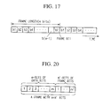
- Figure 20 illustrates an example of bit arrangement in such a frame.
- Encoder 75 performs parallel/serial conversion of m-bit parallel data and m'-bit redundant data output from a redundant data generator 76 to a serial data train in a p-s conversion section 77 at m+m':1 clock rate.
- One apparatus of parallel redundancy encoder 70 is comprised by arranging several encoders 75 in parallel.
- Figure 22 shows a functional block diagram of a parallel redundancy encoder that does not multiplex data for transmission.
- Encoder 75 inserts m' bit of redundant data output from redundant data generator 79 for each m bits of data train input into a frame bit insertion section 78 at a bit speed of f 0 , and encodes the combined data by sending at a bit speed of (m+m')/(m) ⁇ f 0 .
- One parallel redundancy encoder 70 is comprised by arranging several encoders 75 in parallel.
- mB1A coding which adds one auxiliary bit for each m bits of data.
- Variations of mB1A coding include a case of using the auxiliary bit as the parity bit, known as “mB1P coding", and a case of using a coding bit for the preceding bit, known as “mB1C coding”.
- mB1P coding a case of using the auxiliary bit as the parity bit
- mB1C coding a case of using a coding bit for the preceding bit
- 8B10B coding there are encoding methods that do not use frame bits
- Figure 23 shows an example of the conventional channel-to-channel skew compensation apparatus received in the receiver channels that detects and compensate for the skewing amount in data generated by such parallel redundancy encoder described above.
- the channel-to-channel skew compensator shown in Figure 23, pre-selected one channel among the parallel interconnections is designated as the reference group train, i.e., the master channel.
- Master channel frame sync circuit 82 enters master channel input data into the master channel and outputs master channel frame signals (sync signals) to indicate the input data positions along the time axis.
- each frame sync circuit 83 enters own input data into respective channels, and generates frame signals to indicate the input data positions along respective time axes.
- own comparison circuit 84 is provided in all channels other than the master channel.
- Each comparison circuit 84 compares frame signals in own channel with master channel frame signals. In other words, comparison circuit 84 determines how far ahead or behind its own frame signal is compared with the corresponding master frame signal, and outputs advance/delay information as a skew signal.
- Input data into the master channel are delayed by the master channel data delaying circuit 85 for a pre-determined time duration. All input data other than the master channel data are delayed by their own data delaying circuit 86. Each data delaying circuit 86 receives own skew signal, and adjusts the degree of skewing so as to match own frame position to the respective master frame position.
- master channel data delaying circuit 85 does not affect the operating principle. Resulting from such series of adjustment steps, parallel data compensated for channel-to-channel skewing are generated.
- each comparison circuit 84 adjusts the degree of skewing produced by the respective data delaying circuits 86.
- positions (timing) of the data bit train of the skew-compensated data become instantaneously shifted with respect to the master frame positions, thereby creating errors in the transmitted data.
- bit numbers for the reference time point for data in the channel-to-channel skew compensation apparatus change in a sequence such as 1,2,3,4,5,...
- the bit number of the reference time point is 2
- the data for the bit numbers 1,2,4,5,... appear in the data after compensation, which is to say that the bit number 3 disappears.
- bit numbers for the reference time point for data in the channel-to-channel skew compensation apparatus change in a sequence such as 1,2,3,4,5,...
- the bit number of the reference time point is 3
- the data for the bit numbers 1,2,3,3,4,5,... appear in the data after compensation, which is to say that the bit number 3 is replicated.
- master channel may be the channel exhibiting either the maximum delay or the minimum delay.
- data delay in the master channel data delaying circuit 85 may be chosen to be (x+1) bits, then, in channels other than the master channel, it is necessary to select the maximum data delay in the data delay circuit 86 to be (2 ⁇ x+1) bits.
- skew control incorporates a synchronization guard circuit in the channel-to-channel skew compensation apparatus to prevent erroneous operation caused by noise and increase the reliability of frame synchronization.
- a synchronization guard circuit is provided, and signal delay amount is updated in each channel when frame bits are detected contiguously over a certain number of frames at the same timing as inside the frame.
- bit speed of input data is different than the bit speed of output data such that it is necessary to provide two types of clocks operating at different speeds. For this reason, it becomes necessary to provide a PLL circuit (phase-locked loop circuit: phase synchronizing loop circuit), however when a PLL circuit is included in an encoding device, it creates a problem that the circuit size becomes large. Also, PLL circuit must be adjusted to the speed of the drive clock, thus creating a problem that it cannot be operated at any desired clock speed. Furthermore, in the conventional parallel encoding method described above, there is a problem that clock speed conversion circuits become necessary in the receiver-side decoder for deleting redundant data from the transmitted data.
- one object of the present invention relates to a technique of encoding parallel data, and to provide a parallel redundancy encoding apparatus, of a relatively simple construction by eliminating the need for speed conversion circuits, that can respond flexibly to changes in bit speeds.
- Another object is to provide a channel-to-channel skew compensation apparatus that can prevent changes in skewing amount generated in one problem transmission channel from affecting other problem-free transmission channels and to adjust the delay amount in the problem channel by using the skew compensation circuit.
- Further object is to provide a channel-to-channel skew compensation apparatus that can prevent outputting erroneous data by shortening the time span between a state of frame synchronization loss and regaining of a state of frame synchronization to update the signal delay amount.
- the object related to parallel redundancy encoding has been achieved in a parallel redundancy encoding apparatus to encode m channels of parallel data input in synchronization with clock signals, comprising: a redundancy generation section for generating m' channels of redundant data; and a data switching section for accepting m+m' channels of parallel input data, comprised by the m' channels of redundant data added to them channels of the parallel data, and outputting m+m' channels of parallel data by switching data in each channel for every clock signal according to a pre-determined rule.
- the data switching section switches data according to a pre-determined pattern repeated at m+m' clock cycles. It is also preferable that the data switching section switches data so as to output m' clock pulse counts of redundant data between every channels operating at m+m' clock cycles. Further, it is preferable that the data switching section switches data so as to produce a common serial pattern in all output channels, and that each serial pattern output is shifted by one bit in each channel with respect to a common reference time point.
- the apparatus may be operated such that the redundancy data generation section derives m' channels of redundant data from a serial pattern of m channels of data according to a pre-determined rule.
- the present parallel redundancy encoding apparatus to provide stability of direct current level in received signals, detection of channel-to-channel skewing and detection of data errors without the need of a speed conversion section. Because such speed conversion sections are not needed, encoding apparatus is simplified so that the apparatus presents many advantages including compact size, lower power consumption and overall cost. Also, because there is no need for speed conversion circuits which need to be adjusted to a particular operating speed, one parallel encoding apparatus can be operated at any desired clock speed, so that the need for providing a plurality of parallel encoding apparatuses to suit various operating speeds is eliminated. Further, because the encoding apparatus can be operated at any desired speed, it enables to realize an encoding apparatus that can be operated at various speeds to suit changes in the traffic density of transmission data. Such a parallel data encoding system can provide many advantages including lower power consumption.
- a channel-to-channel skew compensation apparatus of the present invention comprising: an N number of frame synchronization circuits (11-1 ⁇ 11-n), provided for each transmission channel used, receiving parallel input data comprised by N parallel bits of not less than two bits located at identical bit-positions arranged on a common time axis, transmitted in parallel over N transmission channels, and generating frame signals (SF) to indicate positions of the parallel data on the common time axis for each operative transmission channel (ch1 ⁇ chn); a reference timing determination circuit (16) for deciding a reference timing according to N pieces of frame signals output from the frame synchronization circuits; a skewing amount detection section (15) for generating N pieces of skewing amount signals (SS) according to the reference timing determined by the reference timing determination circuit; and a timing compensation circuit (13-1 ⁇ 13-n) provided in each transmission channel for adjusting output timing of the parallel data in individual transmission channels according to skewing amount signals generated by the skewing amount detection section
- the N frame signals generated on each of the above transmission channels have no relation to the contents of the data of each transmission channel, and all N frame signals are output from the synchronous frame circuit at the same time.
- the skew compensation apparatus of such a construction has no special channel such as the master channel, but skewing amount is detected and compensated in each transmission channel individually.
- Reference timing required for detecting a skewing amount is determined according to N frame signals output from the frame sync circuit in each channel, thereby eliminating the need for special fixed channel so that the maximum delay amount required in timing compensation section is lessened compared with prior art systems. Therefore, the present system can operate more reliably.
- the timing compensation section only needs to delay the progress of the data by the amount of the clock pulse counts equal to reference timing.
- the maximum delay amount to guarantee skew compensation in all the channels is limited to (x+1) bits for x-bits frame length or the x-bits length of the bit holder.
- the skewing amount detection section and timing compensation section are operating independently in individual channels so that skew problems in one channels does not affect other channels.
- the reference timing determination circuit in the channel-to-channel skew compensation apparatus may include an N number of shift registers (121-1 ⁇ 121-n) to store a plurality of N frame signals (SF-1 ⁇ SF-n) over given clock cycles, and a logic computation section (14) to determine reference timing based on output signals from the shift registers.
- the skewing amount detection section (15) in the channel-to-channel skew compensation apparatus may include a data holding section (122-1 ⁇ 122-n) in each channel for holding signals output from the shift registers (121-1 ⁇ 121-n) at a reference timing determined by the reference timing determination circuit.
- the above construction allows N frame signals in each channel to be stored in the shift register during a plurality of clock cycles, a plurality of frame signals appearing at the common reference time point at different times on the common time axis can be monitored at the same timing. And, when N frame signals are held in the shift register, the data holding section latches the output signals from the shift register, and timing shift between the transmission channels, i.e. skewing, can be detected.
- the logic computation section (14) in the channel-to-channel skew compensation apparatus may include a start signal generation section (124) for generating a start signal (Scs) upon detecting that a frame signal is held in all N number of the shift registers in the reference timing determination circuit; and a counter section (123) for counting a given count of clock pulses according to the start signal and repeatedly output the reference timing signals (Sref) at a period identical to a frame period of the parallel data.
- a start signal generation section (124) for generating a start signal (Scs) upon detecting that a frame signal is held in all N number of the shift registers in the reference timing determination circuit
- a counter section (123) for counting a given count of clock pulses according to the start signal and repeatedly output the reference timing signals (Sref) at a period identical to a frame period of the parallel data.
- this construction allows the data to be input repeatedly to correspond with the frame length.
- the counter section (123) checks one frame period.
- the logic computation section (14) in the channel-to-channel skew compensation apparatus may include a reset signal generation section (125) for stopping operation of the counter section (123), when the counter section is outputting the reference signals (Sref), upon detecting that a frame signal is not held in any one of N shift registers in the reference timing determination circuit.
- the start signal generation section (124) in the channel-to-channel skew compensation apparatus may include a mid-position identify section (1244) for generating a start signal (Scs), upon detecting that a frame signal is held in all N number of the shift registers in the reference timing determination circuit, by identifying a bit-position which appears first on the common time axis as a leading position of the N frame signals, and identifying another bit-position which appears last on the common time axis as a trailing position, so as to output a start signal (Scs) when a mid-position frame between the leading position and the trailing position approaches a middle-bit position of a shift register (121) in individual frame circuits (SF-1 ⁇ SF-n).
- a mid-position identify section (1244) for generating a start signal (Scs), upon detecting that a frame signal is held in all N number of the shift registers in the reference timing determination circuit, by identifying a bit-position which appears first on the common time axis as a leading position of the N
- the reference timing is selected when all N shift registers are holding a frame signal, if the last frame signal is further delayed due to fluctuation occurring in one frame period, there is high probability that some channels cannot be checked for skewing. Therefore, by adopting the above construction, the reference timing is selected when the mid-position of the overall range between the leading frame signal to the trailing frame signal coincides with the middle of the shift register. According to this approach, when the shift amount between the leading and trailing frame signals is sufficiently smaller than the number of bits in the shift register, even in a case of leading bit advancing or trailing bit delaying due to fluctuation caused within a frame period, probability is low that the position of these frames will be outside the holding capability of the shift register. Therefore, this approach minimizes generation of errors of this type.
- the start signal generation section (124) may include a multiple-position identify section (1246) for identifying a frame position on the common time axis that is shared by a maximum number of frame signals among N number of frame signals as a maximum position, so as to output the start signal when a frame signal (SF) on the maximum position approaches the middle-bit position of a shift register (121) in individual frame circuits (SF-1 ⁇ SF-n).
- a multiple-position identify section (1246) for identifying a frame position on the common time axis that is shared by a maximum number of frame signals among N number of frame signals as a maximum position, so as to output the start signal when a frame signal (SF) on the maximum position approaches the middle-bit position of a shift register (121) in individual frame circuits (SF-1 ⁇ SF-n).
- the above construction allows to select the reference timing to be the period between the mid-position of the frame coinciding with the middle-bit of the shift register. And, when the shift amount between the leading and trailing frame signals is sufficiently smaller than the number of bits in the shift register, even in a case of leading bit advancing or trailing bit delaying due to fluctuation caused within a frame period, probability is low that the position of these frames will be outside the holding capability of the shift register. Therefore, this approach minimizes generation of errors of this type.
- the object to provide a channel-to-channel skew compensation apparatus that can shorten the time required to correct frame synchronization loss, caused by fluctuation in channel-to-channel skewing amount, to return to the frame synchronization state to enable to update the signal delay amount is achieved by providing skew compensation during decoding of error correction when the input parallel data have been encoded for error correction.
- parallel data encoded for error correction means not only parallel data encoded by the present redundancy encoding apparatus but also those parallel data encoded by other methods.
- a channel-to-channel skew compensation apparatus comprising: an error correction section (21) receiving parallel data which have been error correction encoded for channel-to-channel positional shifts on the common time axis and decoding error corrections of the parallel data, and generating an error signal to indicate that there is or there is no error in each transmission channel; and a channel-to-channel skew compensation section (20) for adjusting channel-to-channel positional shifts on the common time axis in the parallel input data.
- the apparatus enables to detect bit errors in each channel during the decoding process of error correction encoded parallel data, and when the frequency of error detection is high, amount of skewing correction provided by the channel-to-channel skew compensation section is not appropriate, so that the amount of compensation is altered. On the other hand, if the frequency of error detection is low, the amount of compensation can be considered appropriate. In other words, controlling the channel-to-channel skew compensation section, according to the errors detected by the error correction section, enable channel-to-channel compensation of high reliability.
- control is executed by error signals of high reliability output by the error correction section, so there is no need for checking the synchronization state over a large number of frames. That is, it is not necessary to check the synchronous state over a large number of frames by detecting frame synchronization or frame asynchronization based on error signals because the error signals output from the error correction section are output for every clock pulse, and when the channel-to-channel skewing amount fluctuates, the amount of skewing correction can be renewed very quickly by tracking the change in real-time.
- the channel-to-channel skew compensation apparatus may be comprised by a frame position detection section (22) in each transmission channel for detecting frame positions on a common time axis of the parallel input data; a channel-to-channel skew compensation section (20) for adjusting channel-to-channel positional shifts in the parallel data on the common time axis, based on frame positions in not less than two transmission channels on the common time axis detected by the frame position detection section; an error correction section (21) receiving parallel data that are error correction encoded for channel-to-channel positional shifts on the common time axis, and decoding error corrections provided for the parallel data, and generating an error signal to indicate that there is or there is no error in each transmission channel; and an error control section (23, 24) for controlling a detection state of the frame position detection section according to error signals output by the error correction section.
- frame position detection section detects frame positions in the parallel data in each transmission channel on the common time axis.
- the channel-to-channel skew compensation section adjusts positional shift of parallel data in different channels, according to frame positions in at least two transmission channels, detected by the frame position detection section, that are on the time axis.
- the error correction section receives parallel data corrected for positional shift on the time axis in different channels, and perform error correction decoding, and generates error signals, to indicate there is or there is no error, for each transmission channel.
- the error control section controls the detection state of each frame position detection section according to the error signals output from the error correction section.
- control is executed in real-time by error signals of high reliability output by error correction section to detect the detection state of the frame position detection section, so that there is no need for checking the synchronization state over a large number of frames.
- the amount of skewing correction can be renewed very quickly by tracking the changes in real-time.
- a synchronization guard section (35b1 ⁇ bmax) may be provided in each transmission channel for delaying an adjustment of a positional shift, detected by the frame position detection section, to be applied by the channel-to-channel skew compensation section until specific conditions are fulfilled.
- transmitted signals are affected by noise, so that the reliability of such data as frame bit synchronization signals contained in parallel data is low. Therefore, by renewing the skewing amount according to simplistic synchronization signal only, such a correction process is susceptible to generation of large errors. Therefore, the above synchronization guard section delays applying the amount of skewing compensation detected by the frame position detection section to the channel-to-channel skew compensation section until certain conditions are established. This approach prevents identification of frame position caused by temporary disturbance caused by transient factors such as noise, thereby increasing the reliability of error control.
- a frame loss detection section (23-1 ⁇ 23-N) for the channel-to-channel skew compensation apparatus may be provided in each transmission channel for detecting a frequency of errors generated in each transmission channel, based on error signals output from the error correction section, and outputting a frame loss signal when the frequency of errors exceed a frame loss threshold value.
- the synchronization guard section can identify from the frame loss signals that error generation frequency is higher than the threshold value. Therefore, it considers that frame loss has occurred, and can immediately transfer the operation to adjusting for frame synchronization.
- a frame synchronization detection section (24-1 ⁇ 24-N) may be provided in each transmission channel for detecting a frequency of errors generated in each transmission channel, based on error signals output from the error correction section, and outputting a frame synchronization signal when the frequency of errors exceed a frame synchronization threshold value.
- the synchronization guard section can identify from the frame synchronization signals that error generation frequency is less than the threshold value. Therefore, it considers that frame synchronization is appropriate, and can immediately transfer the operation to renewing the skewing amount.
- Figure 1 is a diagram showing a general configuration of the parallel redundancy encoder.
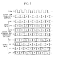
- Figure 3 is a time chart for various operations of the parallel redundancy encoder.
- Figure 4 is a block diagram of a first embodiment of the channel-to-channel skew compensation apparatus.
- FIG. 5 is a block diagram of the skew compensation control unit 12 shown in Figure 4.
- Figure 6 is a block diagram of the main sections of the skew compensation apparatus shown in Figure 4.
- Figure 7 is a time chart showing the operation of counter 123 responding to a start signal Scs.
- Figure 8 is a time chart showing the operation of counter 123 responding to a reset signal Scr.
- Figure 9 is a block diagram of a variation of the timing determination circuit 16 shown in Figure 4.
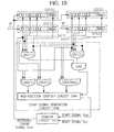
- Figure 10 is a block diagram of the configuration of the start signal generator 124B in a second embodiment of the channel-to-channel skew compensation apparatus.
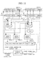
- Figure 11 is a block diagram of the configuration of the start signal generator 124C in a third embodiment of the channel-to-channel skew compensation apparatus.
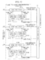
- Figure 12 a block diagram of the channel-to-channel compensation apparatus in a fourth embodiment.
- Figure 13 is a block diagram showing the details of the frame out detection circuit 23 and frame synchronization detection circuit 24 shown in Figure 12.
- Figure 14 is a block diagram of the channel-to-channel compensation apparatus in a fifth embodiment.
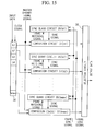
- FIG 15 is a block diagram of the slave channel frame sync circuit 31 shown in Figure 13.
- Figure 16 is a diagram showing the transition of states in the synchronization guard circuit 32.
- Figure 17 is a schematic diagram of an example of frame configuration of input data.
- Figure 18 is a block diagram of the channel-to-channel compensation apparatus in a sixth embodiment.
- Figure 19 is a time chart showing the operation of the master channel frame sync circuit 30.
- Figure 20 is a diagram of an example of frame configuration for m+m' bits.
- Figure 21 is a diagram of a conventional parallel redundancy generator.
- Figure 22 is a diagram of another conventional parallel redundancy generator.
- Figure 23 is a block diagram of a conventional channel-to-channel skew compensation apparatus.
- Figure 1 shows a diagram of a general configuration of the parallel redundancy encoder 1 provided with a redundancy generation section 5 and a data switching section 2.
- Parallel data of m-channels are input, in synchronization with the clock pulses, into the respective channels of the parallel redundancy encoder 1.
- This m-channel parallel input data may also be error correction encoded data to enable detection and correction of data errors in the parallel data at the receiver-side.
- Redundancy generation section 5 outputs m'-channels of redundant data.
- M-channels of parallel data and m'-channels of redundant data are input into a data switching section 2.
- Data switching section 2 monitors output data, over a period of m+m' clock-pulses, and makes certain that every channel (from channel 1 to channel m) contains m'-clock duration of redundant data, and, in the following m+m' clock duration, current output pattern of redundant data is the same as the preceding pattern during the preceding m+m' clock duration, by switching the data in each channel and outputting m+m' channels of data.
- the output data from data switching section 2 contains m' bits of redundant data inserted for every m+m' bits, and all the m channels of data are output at all times.
- the bit speed of the data output to transmission path is the same as the bit speed of input data. Therefore, the parallel redundancy encoder can be operated with one type of clock signal.
- parallel redundancy encoder because redundant data can be deleted by switching data so that speed conversion circuit becomes unnecessary, it enables to provide a parallel redundancy encoder of a simple structure and adaptable to different data speeds.
- parallel redundancy encoders each represented by "a" can be arranged in parallel so that a ⁇ m channels of parallel data and a ⁇ m' channels of redundant data can be switched at m+m' clock cycle to obtain the same result.
- Data switching section 2 is comprised by a 4-clocks counter 3 and four selectors 4-1 ⁇ 4-4.
- Selectors 4-1 ⁇ 4-4 respectively receive input data in three channels chl-ch3 and redundant data (a frame bit F) in one redundancy channel, switches the four groups of input data according to clock signals from the 4-clocks counter 3, and outputs data from four channels.
- Each of the four selectors 4-1 ⁇ 4-4 are operated so as not to select a common input bit at the same time.
- Figure 3 is a time chart for operation of the parallel redundancy encoder shown in Figure 2. Operation of the parallel redundancy encoder will be explained with reference to Figure 3.
- (1) refers to clock signals; (2) to output signals from the 4-clocks counter 3; (3)-(5) to respective input data signals in ch1 ⁇ ch3; (6) to output signals from redundancy generation section 5; and (7) ⁇ (10) to respective output signals from ch1 ⁇ ch4.
- the 4-clocks counter 3 increments the output by one for each one clock pulse starting from [1], and at the fifth clock pulse, the output returns to [1].
- Input data in ch1 is synchronized with the clock signals, and as shown in (3), first clock signal triggers an input of data 1 1 , second clock signal inputs data 1 2 , and the "n"th clock signal inputs data 1 n -Same patterns are repeated for other channels ch2, ch3.
- Selector 4-1 responds to output signals [1] ⁇ [4] from the 4-clocks counter 3 and outputs data ch1 ⁇ ch3 and a frame bit F by switching among the four input channels. The results is a train of bits output from ch 1 as shown in (7). Selectors 4-2, 4-3 and 4-4 operate in the same manner, according to output signals [1] ⁇ [4] from the four-clocks counter 3 to generate output bit train patterns shown in (8) ⁇ (10).
- the resulting output patterns show that the output data from any one channel has one frame bit F (of one bit) inserted at every fourth bit, so that each frame is constituted by a four-bit length. Examining the output data at a particular time slot, it will be noticed that the output data from ch1 ⁇ ch3 are consistent in the same time slot, except for the redundancy channel outputting a redundant bit F.
- optical skewing is produced depending on the magnitude of a mark factor (a ratio of "0" to "1" in data being transmitted), so that a biased mark factor between channels is a cause of generating channel-to-channel skewing.
- encoding is the same in all the channels at the output-side, because the parallel redundancy encoder presented above switches input data in such a way that all the data on the output-side of the channels including the redundant data are uniformly switched, thereby making the mark factor in each channel uniform.
- data symmetry is high in all the outgoing channels, thus preventing the generation of channel-to-channel skewing caused by mark factor biasing and leading to an expectation of scramble effects.
- decoding circuit can also be constructed using only a counter and selectors so that decoding circuit configuration can be simplified, and data delay caused by frame deletion can be avoided. Another advantage is that, because all the channels are subjected to the same encoding process, same frame synchronization circuit can be used in all the channels to lead to highly symmetrical encoding/decoding circuitries.
- Figures 4 ⁇ 8 show the structures and operation of the channel-to-channel skew compensation apparatus.
- Figure 4 is a block diagram of the channel-to-channel skew compensation apparatus.
- Figure 5 is a block diagram of the configuration of the skew compensation control unit 12 shown in Figure 4.
- Figure 6 is a block diagram of the main sections of the skew compensation apparatus shown in Figure 4.
- Figure 7 is a time chart showing the operation of a counter circuit 123 responding to a start signal Scs.
- Figure 8 is a time chart showing the operation of counter circuit 123 responding to a reset signal Scr.
- the channel-to-channel skew compensation apparatus shown in Figure 4 compensates channel-to-channel skewing of parallel data DI(1), DI(2), DI(3), ..., DI(n) input into "n" number of channels ch1, ch2, ch3, ..., chn, and outputs output data DO(1), DO(2), DO(3), ..., DO(n) from each channel.
- the channel-to-channel compensation apparatus includes a frame sync circuit 11 and a data delay circuit 13 for each of the n channels and a skew compensation control unit 12 for the overall apparatus.
- each reference numeral is accompanied by a symbol to indicate a particular channel inside the brackets. Signals in various circuits are treated in the same manner.
- Skew compensation control unit 12 includes a timing determination circuit 16 and a skewing amount detection circuit 15.
- Frame sync circuit 11 synchronizes each input signal (input data Dl) input into respective channels of the channel-to-channel skew compensation apparatus, and outputs corresponding synchronized frame signals SF.
- Input data DI are serial signals, and are divided into a pre-determined frame length before inputting.
- frame sync circuit (sync circuit) 11 detects the position of each frame on the time axis, i.e. its arrival timing.
- a frame signal SF output by the frame sync circuit 11 is a type of sync signal, and is output as a pulse at a timing determined by the detected positions of the frames.
- Skew compensation control unit 12 compares frame signals SF(1) ⁇ SF(n) in all the channels, and identifies skewing amount in respective channels. Amount of channel-to-channel skewing is caused by relative shifts in the data positions, so that a reference timing is required for determining the skewing amount. Because there is no master channel in the present skew compensation apparatus, timing determination circuit 16 decides the reference timing for judging the skewing amount for the frame signals SF(1) ⁇ SF(n) in all the channels.
- Skewing amount detection circuit 15 detects a skewing amount SS(1) ⁇ SS(n) in each channel based on the timing selected by the timing determination circuit 16. Each skewing amount SS(1) ⁇ SS(n) is impressed into each data delay circuit 13 in the respective channels as the skewing amount to be controlled. Data delay circuit 13 in each channel and receives the skewing amount SS output by the skew compensation control unit 12, and adjusts the amount of data delay in each channel so as to adjust frame positions of the data in all the channels.
- FIG. 5 Internal structure of the skew compensation control unit 12 is shown in Figure 5.
- internal structure for only three channels, chl, ch2 and chn, are shown, but those channels which are not shown have the same structure as chl, ch2 and chn.
- the shift registers 121(1) ⁇ 121(n) and the logic computation section 14 are included in the timing determination circuit 16 shown in Figure 4.
- Frame signals SF input by the frame sync circuit 11 shown in Figure 4 are input into a shift register 121 provided in each channel.
- Each shift register 121 can hold [bmax bits] of data.
- Shift register 121 is impressed with a constant periodic clock signal for holding the input frame signal FS and shifting the bit position, but the signal line for the clock signal is omitted in Figure 5.
- a frame signal SF impressed on the input terminal of the shift register 121 is held in the first bit [b1] in synchronization with the clock signal.
- the retained frame signal SF shifts successively to each bit position [b2], [b3], [b4], ..., [bmax].
- Maximum number of bits [bmax] for the shift register 121 is determined freely within the number of bits equal to the frame length of input data DI.
- the range of possible amount of skew compensation is also increased.
- channel-to-channel skew compensation is possible within a range of numbers of bits given by [bmax] less [1] and a duration TC governed by the period of the clock signal.
- this frame signal SF will be held in one of the bit positions [b1] ⁇ [bmax] in the shift register 121. It is therefore possible to identify the relative positions of the bits on the time axis from the bit position of the frame signals SF held in the shift register 121.
- a counter circuit 123 is used to check the amount of skewing in this embodiment by outputting a reference timing signal Sref repeatedly for each frame. As shown in Figure 7, counter circuit 123 counts clock signals while performing channel-to-channel skew compensation, and outputs a reference timing signal Sref at the end of each frame.
- Reference timing used to check the amount of skewing is determined by the start signal generation circuit 124. That is, when the start signal generation circuit 124 shown in Figure 7 outputs a start signal (a pulse signal) Scs, the counter circuit 123 outputs a reference timing signal (a pulse signal) Sref at the end of every frame period.
- a reset signal generation circuit 125 is provided in the logic computation section 14 to stop the operation of the counter circuit 123.
- the reset signal generation circuit 125 outputs a pulse of reset signal Scr, it stops generation of reference timing signal Sref, as shown in Figure 8.
- the frame length in input data DI (frame period) is equal to the pulsing period of the clock signal multiplied by the [MAX] number of bits.
- the reference timing signal Sref output by the logic computation section 14 is impressed as a control signal on data latch 122 in each channel.
- data latch 122 in each channel latches and holds input data.
- Data latch 122 in each channel can hold [bmax] bits of data. Input terminal of the data latch 122 is connected to output terminal of the shift register 121. Therefore, the data latch 122 memorizes a total number of bits ([b1] ⁇ [bmax]) held in the shift register 121.
- a frame signal SF is included in some bit positions of the data memorized in the data latch 122. Also, these bit positions in the data latch 122 correspond to positions on the time axis of the frame signal SF in each channel. Therefore, when there is channel-to-channel skewing in input data DI, data delay times may be adjusted according to the data memorized in data latch 122 to eliminate shifts in data positions (times) from channel to channel. In other words, data memorized in the data latch 122 can be utilized as skewing amount signal SS.
- Counter circuit 123 begins counting upon receiving a start signal Scs and stops counting upon receiving a reset signal Scr, as illustrated in Figures 7 and 8.
- Counter circuit 123 outputs reference timing signals Sref at a period to match the frame length.
- the contents of the shift registers 121 are transferred to data latch 122 at an output timing given by the reference timing signals Sref.
- Data latch 122 in each channel acting as the skewing amount signal SS for own channel, checks the location of the bit position holding the frame signal SF. For example, if the reference bit position is selected to be "m+1"th bit position, and if the frame signal SF is detected at the "m"th bit holding position in the data latch 122, the skewing amount in that channel is judged to be a one-bit-delay. If the frame signal SF is detected at the "m+5"th bit holding position in another channel, the skewing amount in that channel is judged to be a four-bit-advance.
- Start signal generation circuit 124 outputs a start signal Scs when frame signals SF in all the channels are held inside the shift register 121.
- start signal Scs When all the frame signals, from a frame signal having the least amount of delay to the frame signal having the maximum amount of delay, are held in the shift registers 121 of each channel, upon cueing by the start signal Scs, counting action by the counter circuit 123 is started.
- the reset signal generation circuit 125 When a channel is found that has no frame signal SF in the shift register while the reference timing signal Sref is active, the reset signal generation circuit 125 outputs a reset signal Scr. When the reset signal Scr is received, the counter circuit 123 stops counting and waits for an input of a start signal Scs.
- Data delay circuit 13 adjusts data delay amount in each channel according to skewing amount signals SS output by respective data latch 122, thereby compensating channel-to-channel skewing.
- the present channel-to-channel skew compensation apparatus produces an independent compensation action for skewing in each channel, and therefore, when a skewing amount is changed in any channel, change in the skew amount signal SS is limited only to the channel in which skewing amount is changed.
- the maximum value of skewing amount which can be compensated is (bmax-1) bits when the number of bits in the shift register 121 is [bmax]. This means that a relatively large amount of skew compensation, in comparison to the number of bits in the shift register 121 and others, can be provided.
- the signal conditions of all the bits output from the shift register 121 are monitored by the start signal generation circuit 124 and the reset signal generation circuit 125. That is, signals of all the bits ([bmax] bits) output from the first shift register 121(1) are input into or-gate 1241(1) while signals of all the bits output from the second shift register 121(2) are input into or-gate 1241(2) inside the start signal generation circuit 124.
- output signals from or-gate 1241 for all the channels are input into and-gate 1242. If the frame signal SF is held in any of the bit positions in the shift register 121, output of or-gate 1241 becomes active (high level). And, frame signals SF in all the channels are held in any of the bits in respective shift registers 121, output of and-gate 1242 becomes active (high level).
- Output of and-gate 1242 is impressed on the counter circuit 124 as the start signal Scs.
- counter circuit 123 starts counting.
- the counter circuit 123 repeatedly outputs reference timing signals at the same timing as the frame period. In synchronization with the reference timing signal Sref, content of each shift register 121 is transferred to the respective data latch 122.
- Output bits from data latch 122 are input into data delay circuit 13 as the skewing amount signal SS.
- each data delay circuit 13 is comprised by a shift registers 131 for data delaying purpose and a selection circuit 132.
- Data delaying shift register 131 shifts input data DI input into each channel of the channel-to-channel skew compensation apparatus one bit at a time for each pulse of the clock signal (signal line for the clock signal is omitted).
- the selection circuit 132 When the frame signal SF is held in a "k"th bit (k is a natural number less than [bmax] in the data holding circuit 122, i.e., "k"th skewing amount signal is active, the selection circuit 132 outputs data at the "k"th bit of the data delaying shift register 131. Therefore, for the channel with the maximum amount of transfer delay, the frame signal SF is held in the first bit in the data latch 122, and the data in the first bit of the data delaying shift register 131 are output as output data DO from the data delaying circuit 13.
- skewing amount signal SS is not output from the channel not having the frame signal SF so that skew compensation cannot be carried out in the normal manner.
- the reset signal generation circuit 125 sends a reset signal Scr to the counter circuit 123, and resets the counter circuit 123. After resetting, if the shift registers 121 in all the channels hold a SF signal, start signal generation circuit 124 sends a start signal Scs to the counter circuit 123, which re-starts counting to return to normal skew compensation action.
- reset signal generation circuit 125 has an internal start signal generation circuit 124.
- start signal generation circuit 124 shares certain functional elements with reset signal generation circuit 125. Functional aspects of the structure is not different from those shown in Figure 5.
- output of and-gate 1242 becomes active.
- Output of and-gate 1242 is inverted in the inverter 1251 and is impressed on the and-gate 1252.
- Output of an inverter 1251 becomes active when there are more than one channel not having the frame signal SF the shift register 121.
- Output of inverter 1251 and reference timing signal Sref are impressed on the input of and-gate 1252, so that when the reference timing signal Sref is active and a channel not having the frame signal SF is not held in the register 121 is found, reset signal Scr becomes active, and the counter circuit 123 is reset.
- master channel is deleted in this embodiment, and skewing is judged according to reference timing signal Sref output by the counter circuit 123 so that delay amount adjustment in the four data delay circuits 13 is limited to the channel that is experiencing skewing fluctuation regardless of what channel it is generated in.
- delay circuit with [bmax] number of bits, all skewing of less than ([bmax]-1) bits can be compensated using the present skew compensation apparatus.
- skewing amount that can be compensated by the apparatus may include any number of bits (times) up to 1 clock time shorter than one frame length.
- a start signal generation circuit 124B shown in Figure 10 is used instead of the start signal generation circuit 124 used in Embodiment 1.
- Other components are the same as those in Embodiment 1.
- Start signal generation circuit 124B has [bmax] pieces of or-gates 1243 and a mid-position identify circuit 1244.
- suffixes inside the brackets attached to the or-gate 1243 indicate bit-positions, not channels.
- the output bits from the 1-position of shift registers 121 in all the channels are input into the first or-gate 1243(1).
- the output bits from the 2-position ⁇ [bmax]-position from the shift registers 121 in all the channels are input into the corresponding 2nd-or-gate to [bmax]-or-gate 1243.
- Output signals from all the or-gates 1243 are input into the mid-position identify circuit 1244.
- Output signals from the and-gates 1242 are also input into the mid-position identify circuit 1244.
- output signals from and-gates 1242 becomes active when a frame signal is held in the shift registers 121 in all the channels.
- the mid-position identify circuit 1244 selects a bit that is closest to the leading bit and a bit closest to the trailing bit from all the or-gates 1243 whose outputs are active, and when the mid-position between those bits arrives at the mid-point of the bit positions [b1] ⁇ [bmax] in the respective shift register 121, a start signal Scs is output.
- a start signal Scs is generated when the mid-position between the leading and trailing bits reaches (m+1)th bit in the shift register 121. If the difference between the leading and trailing bits is an odd number, a start signal Scs may be output when the mid-position reaches between "m"th bit and "m+1"th bit or "m+1" bit and "m+2" bit in the shift register 121.
- the start signal Scs is output to the counter circuit 123 when frame signals SF are held in the shift registers 121 in all the channels, therefore, if skewing amount fluctuates beyond the limit of the maximum delay channel, it is necessary to reset the counter circuit 123.
- reference timing signal Sref is automatically adjusted so that the mid-point of the frame signals SF of skewed data coincides with the mid-point of the data latch 122. This technique is advantageous because the data latch 122 is more effectively used against skewing fluctuation, and there is less need for resetting the counter circuit 123.
- a start signal generation circuit 124C shown in Figure 11 is used instead of the start signal generation circuit 124 used in Embodiment 1.
- Other components are the same as those in Embodiment 1.
- the start signal generation circuit 124C is provided with [bmax] pieces of adder circuit 1245 and a multiple-position identify circuit 1246.
- the output bits from 1-position of the shift registers 121 in all the channels are input into the first adder circuit 1245 (1). Therefore, the adder circuit 1245 outputs a number of shift registers 121 that hold frame signal SF in the 1-position bit.
- the adder circuits 1245(2) ⁇ 1245(bmax) correspondingly receive signals from the 2-position bit to [bmax]-position bit in the shift registers 121 in all the channels, so that the number of shift registers 121 holding a frame signal SF in the respective bits is output from the adder circuit 1245. All the output signals from the adder circuit 1245 are input into the multiple-position identify circuit 1246.
- Multiple-position identify circuit 1246 compares output of all the adder circuits 1245(1)-1245(bmax) when the output of and-gate 1242 is active.
- a start signal Scs is generated when the number output from the adder circuits 1245, assigned to the mid-position bit between the [1] ⁇ [bmax] bits, shows a maximum. That is, a start signals Scs is generated when frame signals SF are held in the shift registers 121 in all the channels, and the result of a comparison process yields a maximum.
- the comparison process waits for a situation to develop so that the number of channels holding the frame signals SF in the mid-position bit (between [1]-bit and [bmax]-bit) of the shift register 121 becomes higher than the number of channels holding frame signals SF in other bit-positions.
- This technique is advantageous because of more effective utilization of the counter circuit 123. For example, if the skewing amount is considered to follow a statistical distribution involving the number of channels experiencing the fastest data delivery and those experiencing the slowest data delivery, it would be reasonable to assume that the number of channels experiencing some medium delay would be the most prevalent. Therefore, the start signal generation circuit 124C used in Embodiment 3 is adjusted such that the mid-point of the spread of skewing amount which is statistically distributed in a parallel data transfer system, coincides with the mid-position bit in the data latch 122. Therefore, data latch 122 is utilized in the most effective manner, thereby lessening the need for resetting the counter circuit 123.
- Channel-to-channel skew compensation apparatuses which will be presented in the following embodiments are useful when the input parallel data are encoded so that errors in input parallel data are correctable.
- the apparatus checks for any errors in input data, and skew compensation is performed according to the results of checking. It is not necessary that correctably encoded parallel data are limited to those produced by the redundancy generation apparatus presented in the foregoing embodiments.
- the skew compensation apparatus presented below can process parallel data which have been frame encoded by other methods as well as parallel data output from any one of the channel-to-channel skew compensation apparatuses presented above.
- Figure 12 is a block diagram of the apparatus and Figure 13 is a block diagram showing the details of the frame loss detection circuit 23 and the frame sync detection circuit 24.
- this channel-to-channel skew compensation apparatus is comprised by a channel-to-channel skew compensation circuit 20 and an error correction circuit 21.
- Data input into the channel-to-channel skew compensation apparatus are binary data and are already error correction encoded and arranged in N parallel bits.
- N bits of parallel data passes through N channels of different transmission paths for each data, and are input into N channels ch1, ch2, ..., chN, of channel-to-channel skew compensation circuit 20.
- Error correction circuit 21 decodes the error correction coded N channels of data output from the channel-to-channel skew compensation circuit 20. Because encoding of the error correction codes removes redundant data components, the number of parallel bits is reduced. That is, output data from the error correction circuit 21 has N' bits (where N' ⁇ N).
- Error correction circuit 21 detects errors in the output data from the channel-to-channel skew compensation circuit 20. Error correction circuit 21, upon detecting an error, outputs an error signal to the channel in which the error was detected. This error signal is a binary signal to show the presence or absence of errors, and is output for each bit moving in the time series direction of data. Error signal sent to a channel is input into a frame loss detection circuit 23(1 ⁇ N) and a frame sync detection circuit 24(1 ⁇ N), which are provided in each of N channels. As shown in Figure 13, frame loss detection circuit 23 is comprised by a shift register 25, an adder circuit 26 and a comparison circuit 27, and the frame sync detection circuit 24 is comprised by the shared shift register 25, an adder circuit 28 and a comparison circuit 29.
- Frame loss detection circuit 23 and frame sync detection circuit 24 share the same signals output from one shift register 25. Error signal and clock signal are input into the shift register 25. As shown in Figure 13, shift register 25 has data bits [b1, b2, b3, ..., bJ, ..., bK] for holding data. In other words, shift register 25 can hold up to K bits of data, of which J bits are assigned to the frame loss detection circuit 23.
- the shift register 25 accepts an error signal triggered by a clock pulse, and shifts the data held in each bit position backwards.
- information contained in the error signal are successively held in the bit positions of b1, b2, b3, ..., bJ, ..., bK in the shift register 25.
- the clock signal input cycle into the shift register 25 is the same as the processing cycle of data in each channel of the channel-to-channel skew compensation apparatus. Therefore, each time an error signal is generated, information on the error is successively held in the bits in the respective shift registers 25.
- Adder circuit 26 in the frame loss detection circuit 23 receives the data held in bits 1, 2, 3, ..., J in the shift register 25, and outputs a value of their sum. For example, if there are three bits to indicate that errors are present in the error signals held in the range of bits 1 ⁇ J, then the adder circuit 26 outputs a value 3.
- the value output by the adder circuit 26 varies in accordance with the frequency of errors generated in each channel that is detected in the error correction circuit 21.
- the value output by the adder circuit 26 is compared with a pre-determined threshold value A in the comparison circuit 27.
- a frame loss signal output by the comparison circuit 27 is at a 0-level (non-active level), and when the output value from the adder circuit 26 exceeds the threshold value A, a frame loss signal output by the comparison circuit 27 becomes a 1-level (active: frame loss state).
- the adder circuit 28 in the frame synchronization circuit 24 accepts the data held in bits 1, 2, 3, ..., J, ..., K of the shift register 25, and outputs a value of their sum. For example, when an error signal held in the range of bits 1 ⁇ K contains five bits to show that there are errors, the adder circuit 28 output a value 5.
- the value output by the adder circuit 28 varies in accordance with the frequency of errors generated in each channel that have been detected in the error correction circuit 21.
- the value output by the adder circuit 28 is compared with a pre-determined threshold value B in the comparison circuit 29.
- a frame sync signal output by the comparison circuit 29 is at a 0-level (non-active level)
- a frame sync signal output by the comparison circuit 27 becomes a 1-level (active: frame sync state).
- N-channel parallel data input into the channel-to-channel skew compensation apparatus are obtained by encoding N'-channel parallel data according to the following procedure.
- N'-channel parallel data are error correction encoded in the parallel direction to convert to N-channel parallel data.
- Error correction encoded data in each channel are then frame encoded so that the frame length is the same in all the channels.
- N-channel parallel data input into the present channel-to-channel skew compensation apparatus first enter the channel-to-channel skew compensation circuit 20, which synchronizes the frames in the frame sync circuit 22 in each channel, and aligns the leading bits of each frame, thereby outputting skew-compensated data.
- Data compensated for skewing in the channel-to-channel skew compensation circuit 20 are decoded in the error correction circuit 21 to decode the error correction signals.
- error correction encoding is performed in the parallel direction of the data, if there are k error correction codes (k are a natural number), for example, even if there is an error in the data in the maximum-k channel, all the channels having the error can be specified. Therefore, even if synchronization is lost in the maximum-k channel, error-free N'-channel data can be produced.
- Humming code When error correction encoding is performed using 1-error-correction code, Humming code, for example, may be used.
- BCH code When using 2-error-correction code, BCH code, for example, may be used.
- error correction circuit 21 When skewing amount fluctuates, frame synchronization loss occurs in some channels in the frame sync circuit 22. In such a case, error correction circuit 21 outputs an error signal to indicate "error present" at frequent intervals, and the frame loss signal output by the frame loss detection circuit 23 becomes active, and frame sync circuit 22 executes synchronization adjustments.
- frame synchronization or loss of synchronization can be detected by checking if there are errors in the transmitted data. Therefore, there is no need to monitor a plurality of frames to check whether synchronization is being maintained.
- skewing amount fluctuates, loss of frame synchronization can be detected rapidly, and steps to restore frame synchronization can be completed in short time. Therefore, errors generated by fluctuation in skewing amount are output over a shorter period of time, thereby lessening the possibility of generating errors in more channels than can be corrected by the error correction circuit 21 and increasing the reliability of the channel-to-channel skew compensation apparatus.
- a plurality of error correction circuits may be arranged in parallel to construct one error correction circuit 21.
- two BCH decoding circuits using 2-error code (15, 7) may be combined in parallel to enable error correction for a maximum of four channels in 30-channel parallel input data, thus providing an error correction circuit 21 to output 14-channel parallel data.
- Embodiment 5 The structure and operation of the channel-to-channel skew compensation apparatus in Embodiment 5 are shown in Figures 14 ⁇ 17 and Figure 19. The components which are the same as those in Embodiment 4 are referred to by the same reference numerals.
- Figure 14 is a block diagram of the channel-to-channel skew compensation apparatus.
- Figure 15 is a block diagram showing the structure of a slave channel frame sync circuit 31.
- Figure 16 is a state transition diagram of the sync guard circuit 35.
- Figure 17 is a schematic diagram showing an example of the configuration of the input data frame.
- Figure 19 is a time chart showing the operation of the master channel frame sync circuit 30.
- channel 1 of the N channels ch1, ch2, ..., chN of the channel-to-channel skew compensation apparatus is pre-assigned to the master channel and the remaining channels are assigned to slave channels.
- Data input into the master channel ch1 are delayed by a given amount of time delay in the master channel data delay circuit 34.
- Time delay produced by the master channel data delay circuit 34 is represented by the numbers of pulses from a clock (not shown) impressed on the master channel data delay circuit 34, i.e., (m+1) along the time axis when converted into the number of data bits.
- Data input into the individual slave channels ch2-chN are given time delay needed to compensate for channel-to-channel skewing in the slave channel frame sync circuit 31.
- the amount of time delay given in the slave channel frame sync circuit 31 varies according to channel-to-channel skewing amounts, and is determined by the frame positions (timing) of the data in the master channel and the frame positions of the data input into individual slave channels.
- Data given a delay in the master channel data delay circuit 34 are input into the master channel frame sync circuit 30, which is provided with a frame counter 32, a received frame detection circuit 33 and a sync guard circuit 35.
- master channel frame sync circuit 30 Data input into master channel frame sync circuit 30 are input into the received frame detection circuit 33, which checks for frame bit bF (refer to Figure 17) included in each frame of input data.
- the received frame detection circuit 33 receives rear guarding state signal output from the sync guard circuit 35 and frame signals output from the frame counter 32.
- Received frame detection circuit 33 detects frame bits bF contained in the input data.
- the sync guard circuit 35 When the sync guard circuit 35 is in a hunting state (will be explained later), indicating that neither frame sync signal nor rear guarding state signal is input into the received frame detection circuit 33, the frame counter 32 outputs frame matching signals at a timing to synchronize with the frame bits bF.
- the received frame detection circuit 35 When the sync guard circuit 35 is not in the hunting state, in other words, the received frame detection circuit 35 has an input of either a rear guarding state signal or a frame sync signal, the received frame detection circuit 33 outputs a frame matching signal when the timing of active frame signals matches the timing of receiving of frame bits.
- the sync protection circuit 35 receives frame sync signals output by the frame sync detection circuit 24 and frame loss signals output by the frame loss detection circuit 23.
- Operating state of the sync guard circuit 35 in providing synchronization guarding operation, changes as shown in the state transition diagram shown in Figure 16.
- the state transition diagram special features are found in the manner of transition response to input of frame loss signals and frame sync signals. If a frame loss signal is input by the frame loss detection circuit 24 when the sync guard circuit 35 is in sync guarding state, it immediately changes to the hunting state (non-sync state). And, if a frame sync signal is input by the frame sync detection circuit 25 when the sync guard circuit 35 is in the rear guarding state, it immediately changes to the synchronization state.
- Sync guard circuit 35 outputs rear guarding state signals when its internal state is in the rear guarding state shown in Figure 16, and outputs sync signals when the internal state is in the sync state or front guarding state.
- Frame counter 32 connected to the sync guard circuit 35 begins counting the clock (not shown) at in synchronization with the rear guarding state signal becoming active, and outputs a frame signal for every count of clock pulses equal to the frame length m.
- frame counter 32 When the sync signal becomes active, frame counter 32 outputs frame position signals at the same timing as the master channel frame signals.
- the frame matching signal becomes [0] over contiguous k2-frames or when the frame loss signal becomes [1]
- sync guard circuit 35 goes to the hunting state, and the sync signal becomes non-active, the frame counter 32 is reset and counting is stopped.
- the master channel frame sync circuit 30 outputs frame signals for the master channel. Frame position signals for the master channel are impressed on each salve frame sync circuit 31.
- this slave channel frame sync circuit 31 is provided with a shift register 36 capable of holding data of [bmax] number of bits.
- the number of bits [bmax] held in the shift register 36 is determined by the delay amount (number of bits), and is equal to (2 ⁇ m+1) when the delay amount is (m+1).
- Shift register 36 holds data in synchronization with the clock signals operating at the same timing as the bit rate of input data, and shifts data position one bit at a time for each clock pulse. That is, input data is first held in bit position bl, and the position holding this bit is shifted to bit positions b2, b3, b4 ... for each pulse of a clock signal. Output data from the shift register 36 can be delayed by a maximum of about twice the delay amount that can be provided by the master channel data delay circuit 34.
- comparison circuits 37(b1 ⁇ bmax) and sync guard circuits 35(b1 ⁇ bmax) are provided. Data output from each bit in the shift register 36 are input into respective comparison circuit 37(b1 ⁇ bmax). Each of these comparison circuits 37(b1 ⁇ bmax) receives output data from each bit in the shift register 36 and frame position signals from the master channel.
- each comparison circuit 37(b1 ⁇ bmax) When frame position signal of the master channel is active, each comparison circuit 37(b1 ⁇ bmax) outputs a frame matching signal upon receiving a frame bit from the shift register 36 to the respective sync guard circuit 35(b1 ⁇ bmax).
- Sync guard circuit 32(b1 ⁇ bmax) included in the slave channel frame sync circuit 31 follows the state transition shown in Figure 16, as in the case of the sync guard circuit 35.
- Sync guard circuit 35(b1 ⁇ bmax) outputs a sync signal when synchronized to respective comparison circuits 37(b1 ⁇ bmax).
- Comparison circuit 37(b1 ⁇ bmax) upon receiving respective sync signal, outputs data input from the shift register 36.
- Selection circuit 38 outputs data from a particular comparison circuit 37(b1 ⁇ bmax) that received sync signals.
- Error correction circuit 21 shown in Figure 14 performs error correction in the N-channel parallel data output from the channel-to-channel skew compensation circuit 20 and outputs error corrected data as output data. If there is an error, it further outputs an error signal to the error signal line of the channel having the error. Error signal is input into frame loss detection circuit 23 and frame sync detection circuit 24 provided in each channel. This construction is the same as that used in Embodiment 1.
- the present channel-to-channel skew compensation apparatus shown in Figure 14 can judge frame loss or frame sync from the frequency of error generation; therefore, frame loss can be detected quickly relative to the approach of observing a plurality of frames, and sync recovery can also be determined quickly, thereby shortening the duration of outputting erroneous data.
- FIG 18 The structure of the channel-to-channel skew compensation apparatus in Embodiments 6 is shown in Figure 18.
- the frame sync circuit 51 which is provided in each channel, has the same construction as the master channel frame sync circuit 30 shown in Figure 14.
- Frame sync circuit 51 outputs frame signals by following the same actions as the master channel frame sync circuit 30.
- Skew compensation control uniut 52 receives frame signals output from each channel in the frame sync circuit 51, and judges a skewing amount in various channels by relative comparison of the frame signals received from all the channels, and outputs a skew signal for a particular channel.
- the data delay circuit 53 in each channel provides a delay amount to the data passing through the channel, according to the skew signal output from the skew compensation control uniut 52.
- channel-to-channel skew compensation circuit 20C outputs skew-compensated parallel data from N-channels.
- Error correction circuit 21 connected to the channel-to-channel skew compensation circuit 20C performs in the same manner as in Embodiments 4 and 5. That is, error correction codes are decoded for the N-channel parallel data output from the channel-to-channel skew compensation circuit 20C, which outputs error corrected data as output data. Error signals are sent to the channels which produced respective errors.
- Error signal is input into the frame loss detection circuit 23 and frame sync detection circuit 24 in each channel, which are constructed in the same way as those in Embodiment 4.
- Frame loss signal output by the frame loss detection circuit 23 and frame sync signal output by the frame sync detection circuit 24 are input into the sync guard circuit 35 included in the frame sync circuit 51.
- Sync guard circuit 35 performs sync guarding action according to the transition diagram shown in Figure 16.
- error correction circuit 21 assures error-free output data.
Landscapes
- Engineering & Computer Science (AREA)
- Power Engineering (AREA)
- Computer Networks & Wireless Communication (AREA)
- Signal Processing (AREA)
- Theoretical Computer Science (AREA)
- Synchronisation In Digital Transmission Systems (AREA)
- Error Detection And Correction (AREA)
- Dc Digital Transmission (AREA)
- Communication Control (AREA)
Applications Claiming Priority (6)
| Application Number | Priority Date | Filing Date | Title |
|---|---|---|---|
| JP3261898 | 1998-02-16 | ||
| JP3261898 | 1998-02-16 | ||
| JP5954298 | 1998-03-11 | ||
| JP5954298 | 1998-03-11 | ||
| JP7778398 | 1998-03-25 | ||
| JP7778398 | 1998-03-25 |
Publications (2)
| Publication Number | Publication Date |
|---|---|
| EP0936785A2 true EP0936785A2 (de) | 1999-08-18 |
| EP0936785A3 EP0936785A3 (de) | 2004-01-21 |
Family
ID=27287782
Family Applications (1)
| Application Number | Title | Priority Date | Filing Date |
|---|---|---|---|
| EP99400357A Withdrawn EP0936785A3 (de) | 1998-02-16 | 1999-02-15 | Verschiebungsausgleich für parallele Übertragung |
Country Status (5)
| Country | Link |
|---|---|
| US (2) | US6336192B1 (de) |
| EP (1) | EP0936785A3 (de) |
| JP (1) | JP3193352B2 (de) |
| KR (2) | KR100335604B1 (de) |
| TW (1) | TW419924B (de) |
Families Citing this family (73)
| Publication number | Priority date | Publication date | Assignee | Title |
|---|---|---|---|---|
| US6480548B1 (en) * | 1997-11-17 | 2002-11-12 | Silicon Graphics, Inc. | Spacial derivative bus encoder and decoder |
| US7564283B1 (en) | 1998-06-22 | 2009-07-21 | Xilinx, Inc. | Automatic tap delay calibration for precise digital phase shift |
| JP3699863B2 (ja) * | 1999-07-12 | 2005-09-28 | 株式会社日立コミュニケーションテクノロジー | エラー訂正符号装置、エラー訂正符号復号装置および伝送装置 |
| JP3742257B2 (ja) * | 1999-09-13 | 2006-02-01 | 富士通株式会社 | 復調装置 |
| US7209178B1 (en) * | 1999-09-21 | 2007-04-24 | Samsung Electronics, Co., Ltd. | Optical transfer system having a transmitter and a receiver |
| US7031420B1 (en) * | 1999-12-30 | 2006-04-18 | Silicon Graphics, Inc. | System and method for adaptively deskewing parallel data signals relative to a clock |
| US6889357B1 (en) * | 2000-05-10 | 2005-05-03 | Micron Technology, Inc. | Timing calibration pattern for SLDRAM |
| US7123616B2 (en) | 2000-06-09 | 2006-10-17 | Ixia | Determining round-trip time delay |
| US7187742B1 (en) * | 2000-10-06 | 2007-03-06 | Xilinx, Inc. | Synchronized multi-output digital clock manager |
| US20020104053A1 (en) * | 2000-12-15 | 2002-08-01 | Mike Lei | In-band FEC encoder for sonet |
| US20020091885A1 (en) * | 2000-12-30 | 2002-07-11 | Norm Hendrickson | Data de-skew method and system |
| US20020093986A1 (en) * | 2000-12-30 | 2002-07-18 | Norm Hendrickson | Forward data de-skew method and system |
| US7050512B1 (en) * | 2001-01-08 | 2006-05-23 | Pixelworks, Inc. | Receiver architecture |
| US20020120902A1 (en) * | 2001-02-23 | 2002-08-29 | Alcatel | Method and system for frame synchronous forward error correction |
| US7095817B2 (en) * | 2001-05-03 | 2006-08-22 | Coreoptics, Inc. | Method and apparatus for compensating for timing variances in digital data transmission channels |
| US6965651B1 (en) * | 2001-05-11 | 2005-11-15 | Micrel, Inc. | Method and apparatus for delay adjustment and channel reordering in baseband communication receiving system |
| US20030039226A1 (en) * | 2001-08-24 | 2003-02-27 | Kwak Joseph A. | Physical layer automatic repeat request (ARQ) |
| US6907552B2 (en) * | 2001-08-29 | 2005-06-14 | Tricn Inc. | Relative dynamic skew compensation of parallel data lines |
| US7012935B2 (en) * | 2002-05-16 | 2006-03-14 | Intel Corporation | Alignment and deskew device, system and method |
| US7359407B1 (en) * | 2002-08-27 | 2008-04-15 | Cypress Semiconductor Corp. | Data interface that is configurable into separate modes of operation for sub-bit de-skewing of parallel-fed data signals |
| JP4168439B2 (ja) * | 2002-09-17 | 2008-10-22 | 富士ゼロックス株式会社 | 信号伝送システム |
| US7551640B1 (en) * | 2002-09-20 | 2009-06-23 | Cisco Technology, Inc. | Method and apparatus for errorless frame timing adjustment |
| US7137937B2 (en) | 2002-10-07 | 2006-11-21 | Ellen Croft | Collapsible resistance exercise device |
| GB2395405B (en) * | 2002-11-11 | 2005-11-09 | Phyworks Ltd | Data transmission interface |
| US7653315B2 (en) | 2003-01-21 | 2010-01-26 | Gateway, Inc. | Bi-directional optical monitor interconnect |
| US7496780B2 (en) * | 2003-02-11 | 2009-02-24 | Agere Systems Inc. | Reduction of data skew in parallel processing circuits |
| KR20060027342A (ko) * | 2003-06-17 | 2006-03-27 | 코닌클리케 필립스 일렉트로닉스 엔.브이. | 2차원 광 기록을 위한 채널 동기화 |
| JP4431113B2 (ja) * | 2003-11-14 | 2010-03-10 | 株式会社日立コミュニケーションテクノロジー | データ伝送方法及びデータ伝送装置 |
| JP2005244479A (ja) * | 2004-02-25 | 2005-09-08 | Fujitsu Ltd | 伝送装置 |
| US6999891B2 (en) * | 2004-02-27 | 2006-02-14 | Ixia | Independent deskew lane |
| JP4416789B2 (ja) * | 2004-05-28 | 2010-02-17 | パナソニック株式会社 | 信号受信回路及び信号入力検知回路 |
| JP4260688B2 (ja) | 2004-06-09 | 2009-04-30 | 富士通株式会社 | データ送信装置、データ送受信システム、データ送信装置の制御方法およびデータ送受信システムの制御方法 |
| TWI257482B (en) * | 2004-12-15 | 2006-07-01 | Spirox Corp | Method and apparatus for measuring jitter of signal |
| KR20060081522A (ko) | 2005-01-10 | 2006-07-13 | 삼성전자주식회사 | 피씨아이 익스프레스의 바이트 스큐 보상방법 및 이를위한 피씨아이 익스프레스 물리 계층 수신기 |
| KR100707437B1 (ko) * | 2005-03-03 | 2007-04-13 | 엘지전자 주식회사 | 다중경로 수신신호의 지연을 보상하는 이동통신 시스템 |
| US9384818B2 (en) | 2005-04-21 | 2016-07-05 | Violin Memory | Memory power management |
| US9286198B2 (en) | 2005-04-21 | 2016-03-15 | Violin Memory | Method and system for storage of data in non-volatile media |
| US8112655B2 (en) * | 2005-04-21 | 2012-02-07 | Violin Memory, Inc. | Mesosynchronous data bus apparatus and method of data transmission |
| CN103116565A (zh) * | 2005-04-21 | 2013-05-22 | 提琴存储器公司 | 可配置的开关原件、互连网络及布局网络间相互连接方法 |
| US9582449B2 (en) | 2005-04-21 | 2017-02-28 | Violin Memory, Inc. | Interconnection system |
| US8452929B2 (en) * | 2005-04-21 | 2013-05-28 | Violin Memory Inc. | Method and system for storage of data in non-volatile media |
| KR100656377B1 (ko) | 2005-09-28 | 2006-12-11 | 한국전자통신연구원 | 다중 채널 데이터 검증 장치 및 방법 |
| JP4523540B2 (ja) * | 2005-11-30 | 2010-08-11 | 三菱電機株式会社 | 光受信装置 |
| US7516349B2 (en) * | 2005-12-29 | 2009-04-07 | Intel Corporation | Synchronized memory channels with unidirectional links |
| JP5034329B2 (ja) * | 2006-06-09 | 2012-09-26 | 富士通株式会社 | デスキュー装置およびデスキュー方法 |
| US7546494B2 (en) * | 2006-08-03 | 2009-06-09 | Avalon Microelectronics Inc. | Skew-correcting apparatus using dual loopback |
| US7760836B2 (en) * | 2006-08-03 | 2010-07-20 | Avalon Microelectronics, Inc. | Skew-correcting apparatus using external communications element |
| US7536579B2 (en) * | 2006-08-03 | 2009-05-19 | Avalon Microelectronics, Inc. | Skew-correcting apparatus using iterative approach |
| US8028186B2 (en) * | 2006-10-23 | 2011-09-27 | Violin Memory, Inc. | Skew management in an interconnection system |
| KR100885294B1 (ko) | 2006-12-05 | 2009-02-23 | 한국전자통신연구원 | 다양한 데이터양을 가지는 고속데이터들간의 인터페이스변환 방법 및 장치 |
| US8037370B2 (en) * | 2007-05-02 | 2011-10-11 | Ati Technologies Ulc | Data transmission apparatus with information skew and redundant control information and method |
| KR100901704B1 (ko) * | 2007-08-16 | 2009-06-08 | 한국전자통신연구원 | 다양한 데이터 양을 가지는 고속 데이터 송수신 장치 |
| JP5230367B2 (ja) * | 2008-06-03 | 2013-07-10 | 日本電信電話株式会社 | パラレル光伝送装置及び方法 |
| JP5203153B2 (ja) * | 2008-11-28 | 2013-06-05 | 日本電信電話株式会社 | パラレル伝送方法及びパラレル伝送装置 |
| US8199782B2 (en) | 2009-02-20 | 2012-06-12 | Altera Canada Co. | Method of multiple lane distribution (MLD) deskew |
| CN102396170A (zh) | 2009-04-16 | 2012-03-28 | 日本电气株式会社 | 检测并行信号之间时滞的方法和系统 |
| JP5381305B2 (ja) | 2009-05-08 | 2014-01-08 | 富士通株式会社 | 受信装置、送受信装置、及び伝送システム |
| WO2010137507A1 (ja) * | 2009-05-28 | 2010-12-02 | 三菱電機株式会社 | 通信装置 |
| CN101902271B (zh) * | 2009-05-31 | 2013-03-06 | 国际商业机器公司 | 扭斜检测方法和设备及高速光通信接口 |
| JP5461963B2 (ja) * | 2009-11-11 | 2014-04-02 | アンリツ株式会社 | デスキュー回路及びエラー測定装置 |
| JP5553153B2 (ja) * | 2010-05-10 | 2014-07-16 | 住友電気工業株式会社 | Pon光通信システム用中継方法並びにこの方法を用いたpon光通信システム用中継器及びpon光通信システム |
| JP2011259128A (ja) * | 2010-06-08 | 2011-12-22 | Nec Corp | デジタルデータ伝送システム、送信装置、受信装置、及び伝送方式 |
| JP5525942B2 (ja) * | 2010-07-06 | 2014-06-18 | アンリツ株式会社 | 先頭レーン検出回路及び方法並びにデスキュー回路及び方法 |
| JP2014511578A (ja) | 2011-02-28 | 2014-05-15 | 日本電気株式会社 | モニタ機能を備えた光通信システム及びそのためのモニタ方法 |
| CN103502965A (zh) * | 2011-04-25 | 2014-01-08 | 松下电器产业株式会社 | 信道间时滞调整电路 |
| JP2012257047A (ja) * | 2011-06-08 | 2012-12-27 | Fujitsu Ltd | パラレルシリアル変換回路、情報処理装置及び情報処理システム |
| TWI482477B (zh) * | 2011-12-30 | 2015-04-21 | Bold Team Man Ltd | Wireless digital communication system and its data rate error compensation method |
| US9264023B2 (en) | 2013-08-30 | 2016-02-16 | Cavium, Inc. | Scannable flop with a single storage element |
| US9130549B2 (en) * | 2013-08-30 | 2015-09-08 | Cavium, Inc. | Multiplexer flop |
| JP2018186352A (ja) * | 2017-04-24 | 2018-11-22 | 株式会社東芝 | 通信中継システム及び方法 |
| US10908636B2 (en) * | 2017-10-31 | 2021-02-02 | Sandisk Technologies Llc | Skew correction for source synchronous systems |
| TWM609659U (zh) * | 2020-04-30 | 2021-03-21 | 神亞科技股份有限公司 | 時序誤差的偵測電路 |
| CN114826471B (zh) * | 2022-04-14 | 2025-07-11 | 烽火通信科技股份有限公司 | 一种多通道ptp时戳提取方法和系统 |
Family Cites Families (23)
| Publication number | Priority date | Publication date | Assignee | Title |
|---|---|---|---|---|
| US3708783A (en) * | 1971-06-18 | 1973-01-02 | Ampex | Interchannel time displacement correction method and apparatus |
| US3909711A (en) | 1971-07-28 | 1975-09-30 | Sandco Ltd | Transducer for sensing a variation of a magnetic field on a conveyor belt |
| US3909721A (en) * | 1972-01-31 | 1975-09-30 | Signatron | Signal processing system |
| JPS6030026B2 (ja) | 1975-12-17 | 1985-07-13 | 株式会社日立製作所 | スキユー補正回路 |
| US4275457A (en) | 1977-05-18 | 1981-06-23 | Martin Marietta Corporation | Apparatus and method for receiving digital data at a first rate and outputting the data at a different rate |
| JPS6256040A (ja) * | 1985-09-04 | 1987-03-11 | Fujitsu Ltd | 遅延時間補償回路 |
| NZ220548A (en) * | 1986-06-18 | 1990-05-28 | Fujitsu Ltd | Tdm frame synchronising circuit |
| JPH01278139A (ja) * | 1988-04-30 | 1989-11-08 | Fujitsu Ltd | マルチフレーム同期・変換方式 |
| JP2961743B2 (ja) | 1989-04-14 | 1999-10-12 | 日本電気株式会社 | 高速データ伝送装置 |
| US5068813A (en) * | 1989-11-07 | 1991-11-26 | Mts Systems Corporation | Phased digital filtering in multichannel environment |
| JPH04178047A (ja) | 1990-11-13 | 1992-06-25 | Fujitsu Ltd | スキュー補償方式 |
| JPH0537580A (ja) | 1991-08-01 | 1993-02-12 | Fujitsu Ltd | 並列伝送における信号同期方式 |
| JP3244543B2 (ja) | 1991-12-17 | 2002-01-07 | 富士通株式会社 | 並列伝送処理方式 |
| US5267240A (en) * | 1992-02-20 | 1993-11-30 | International Business Machines Corporation | Frame-group transmission and reception for parallel/serial buses |
| JP3260862B2 (ja) | 1992-10-29 | 2002-02-25 | 株式会社リコー | パラレルデータ伝送装置 |
| JP3227894B2 (ja) | 1993-04-23 | 2001-11-12 | 富士通株式会社 | 並列直列変換装置 |
| JP2694807B2 (ja) * | 1993-12-16 | 1997-12-24 | 日本電気株式会社 | データ伝送方式 |
| US5742907A (en) * | 1995-07-19 | 1998-04-21 | Ericsson Inc. | Automatic clear voice and land-line backup alignment for simulcast system |
| JPH09247140A (ja) | 1996-03-08 | 1997-09-19 | Mitsubishi Electric Corp | インタコネクション装置 |
| US5761209A (en) * | 1996-03-15 | 1998-06-02 | Nec Corporation | Method of transmitting digital signals, transmitter and receiver used therefor |
| JP3031249B2 (ja) | 1996-06-26 | 2000-04-10 | 日本電気株式会社 | 並列データ位相同期回路 |
| JP3209720B2 (ja) | 1997-08-04 | 2001-09-17 | 松下電器産業株式会社 | 複数伝送線路間の遅延時間の調整装置及び調整方法 |
| JP3387379B2 (ja) | 1997-09-01 | 2003-03-17 | 富士通株式会社 | パラレルデータスキュー検出回路 |
-
1999
- 1999-02-12 US US09/249,488 patent/US6336192B1/en not_active Expired - Fee Related
- 1999-02-12 TW TW088102301A patent/TW419924B/zh not_active IP Right Cessation
- 1999-02-13 KR KR1019990007619A patent/KR100335604B1/ko not_active Expired - Fee Related
- 1999-02-15 EP EP99400357A patent/EP0936785A3/de not_active Withdrawn
- 1999-02-16 JP JP03784299A patent/JP3193352B2/ja not_active Expired - Fee Related
-
2001
- 2001-07-20 KR KR1020010043907A patent/KR100352453B1/ko not_active Expired - Fee Related
- 2001-11-09 US US09/986,526 patent/US6557110B2/en not_active Expired - Fee Related
Also Published As
| Publication number | Publication date |
|---|---|
| KR100352453B1 (ko) | 2002-09-11 |
| TW419924B (en) | 2001-01-21 |
| JP3193352B2 (ja) | 2001-07-30 |
| KR100335604B1 (ko) | 2002-05-08 |
| KR19990073017A (ko) | 1999-09-27 |
| US6557110B2 (en) | 2003-04-29 |
| JPH11341102A (ja) | 1999-12-10 |
| US6336192B1 (en) | 2002-01-01 |
| US20020029355A1 (en) | 2002-03-07 |
| EP0936785A3 (de) | 2004-01-21 |
| KR20010089905A (ko) | 2001-10-13 |
Similar Documents
| Publication | Publication Date | Title |
|---|---|---|
| US6336192B1 (en) | Parallel redundancy encoding apparatus | |
| US5251210A (en) | Method and apparatus for transforming low bandwidth telecommunications channels into a high bandwidth telecommunication channel | |
| JP3233801B2 (ja) | ビット位相同期回路 | |
| EP2140589B1 (de) | Verfahren zum synchronisieren von daten | |
| JPH02247709A (ja) | スキユー除去方法 | |
| US6735735B1 (en) | Forward error correcting code encoding equipment, forward error correcting code decoding equipment, and transmission apparatus | |
| US7242736B2 (en) | Data transfer | |
| US20030037297A1 (en) | Frame synchronization device and frame synchronization method | |
| US20030131301A1 (en) | Data transmission system | |
| US6920603B2 (en) | Path error monitoring method and apparatus thereof | |
| US7953095B2 (en) | Transmission system and transmission method | |
| JPH07110004B2 (ja) | 信号路切り換え方法とその装置およびその装置を複数備えたシステム | |
| US6377645B1 (en) | Method and apparatus for controlling bit slippage in high-speed communications systems | |
| US9143420B2 (en) | Data transport system, receiver and transmitter | |
| US6819683B2 (en) | Communications system and associated deskewing and word framing methods | |
| US7058090B1 (en) | System and method for paralleling digital wrapper data streams | |
| JP4183535B2 (ja) | フレーム信号の速度変換処理を行なう光信号伝送装置 | |
| US20030235215A1 (en) | Apparatus and method for aggregation and transportation for plesiosynchronous framing oriented data formats | |
| GB2343092A (en) | Framing codes for a high speed parallel data bus | |
| KR960000934B1 (ko) | 포워드 에러 정정 기술을 사용하는 전송 시스템 | |
| KR20040014822A (ko) | 통신 시스템의 데이터 전송장치에서 클럭 발생기 절환장치 및 방법 | |
| KR20020088550A (ko) | 패킷 동기를 고려한 고속 패킷 데이터의 시간 역다중 회로 | |
| JPH0736547B2 (ja) | ワードインターリーブ方式多重信号の分離装置 | |
| JPH04103235A (ja) | フレームパターン生成方式 | |
| HK1042181A1 (en) | Method of synchronising data |
Legal Events
| Date | Code | Title | Description |
|---|---|---|---|
| PUAI | Public reference made under article 153(3) epc to a published international application that has entered the european phase |
Free format text: ORIGINAL CODE: 0009012 |
|
| AK | Designated contracting states |
Kind code of ref document: A2 Designated state(s): AT BE CH CY DE DK ES FI FR GB GR IE IT LI LU MC NL PT SE |
|
| AX | Request for extension of the european patent |
Free format text: AL;LT;LV;MK;RO;SI |
|
| PUAL | Search report despatched |
Free format text: ORIGINAL CODE: 0009013 |
|
| AK | Designated contracting states |
Kind code of ref document: A3 Designated state(s): AT BE CH CY DE DK ES FI FR GB GR IE IT LI LU MC NL PT SE |
|
| AX | Request for extension of the european patent |
Extension state: AL LT LV MK RO SI |
|
| 17P | Request for examination filed |
Effective date: 20040224 |
|
| 17Q | First examination report despatched |
Effective date: 20040421 |
|
| AKX | Designation fees paid |
Designated state(s): DE FR GB |
|
| 17Q | First examination report despatched |
Effective date: 20040421 |
|
| STAA | Information on the status of an ep patent application or granted ep patent |
Free format text: STATUS: THE APPLICATION IS DEEMED TO BE WITHDRAWN |
|
| 18D | Application deemed to be withdrawn |
Effective date: 20070720 |