EP0943387A1 - Systeme d'alimentation electrique pour ensembles d'usinage par etincelle - Google Patents
Systeme d'alimentation electrique pour ensembles d'usinage par etincelle Download PDFInfo
- Publication number
- EP0943387A1 EP0943387A1 EP98936739A EP98936739A EP0943387A1 EP 0943387 A1 EP0943387 A1 EP 0943387A1 EP 98936739 A EP98936739 A EP 98936739A EP 98936739 A EP98936739 A EP 98936739A EP 0943387 A1 EP0943387 A1 EP 0943387A1
- Authority
- EP
- European Patent Office
- Prior art keywords
- power source
- workpiece
- switching element
- pulses
- machining
- Prior art date
- Legal status (The legal status is an assumption and is not a legal conclusion. Google has not performed a legal analysis and makes no representation as to the accuracy of the status listed.)
- Granted
Links
Images


Classifications
-
- B—PERFORMING OPERATIONS; TRANSPORTING
- B23—MACHINE TOOLS; METAL-WORKING NOT OTHERWISE PROVIDED FOR
- B23H—WORKING OF METAL BY THE ACTION OF A HIGH CONCENTRATION OF ELECTRIC CURRENT ON A WORKPIECE USING AN ELECTRODE WHICH TAKES THE PLACE OF A TOOL; SUCH WORKING COMBINED WITH OTHER FORMS OF WORKING OF METAL
- B23H1/00—Electrical discharge machining, i.e. removing metal with a series of rapidly recurring electrical discharges between an electrode and a workpiece in the presence of a fluid dielectric
- B23H1/02—Electric circuits specially adapted therefor, e.g. power supply, control, preventing short circuits or other abnormal discharges
- B23H1/022—Electric circuits specially adapted therefor, e.g. power supply, control, preventing short circuits or other abnormal discharges for shaping the discharge pulse train
Definitions
- the present invention relates to an electric discharge machining power source unit for an electric discharge machine.
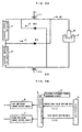
- the positive terminal of a DC power source 10 and a workpiece W are connected through a first switching element T11, while the negative terminal of the DC power source 10 and a machining electrode P are connected through a second switching element T12. Further, the negative terminal of the DC power source 10 and the workpiece W are connected through a reversely-connected first diode D11, while the positive terminal of the DC power source 10 and the machining electrode P are connected through a reversely-connected second diode D12.
- the first and second switching elements T11 and T12 are formed of an FET each. As shown in FIG. 7B, their respective gates G11 and G12 are controlled by means of a first switching element driver circuit 11 and a second switching element driver circuit 12, respectively.
- the first and second switching element driver circuits 11 and 12 are driven by means of pulses with a given pulse width delivered from a pulse signal generator circuit 13 for current peak value setting.
- the pulses with the set width are delivered from the pulse signal generator circuit 13 for current peak value setting. These pulses are applied to the respective FET gates G11 and G12 of the first and second switching elements T11 and T12 through the first and second switching element driver circuits 11 and 12, thereby turning on both these switching elements T11 and T12.
- the workpiece W is subjected to electric discharge machining using the current J0 (machining current) that flows between the workpiece W and the machining electrode P in this manner.
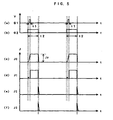
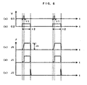
- FIGS. 8 and 9 there will be described discharge currents (machining currents) that are obtained when the power source unit shown in FIGS. 7A and 7B is operated in the aforesaid manner.
- FIG. 8 shows current waveforms for the case where the voltage of the DC power source is raised, and FIG. 9 for the case when the voltage of the DC power source 10 is lowered.
- both the first and second switching elements T11 and T12 are turned on by means of pulse signals (with a pulse width t1) from the pulse-signal generator circuit 13 for current peak value setting (see (a) and (b) of FIG. 8 and (a) and (b) of FIG. 9)
- the voltage of the DC power source 10 is applied between the workpiece W and the machining electrode P.
- the current J0 that flows between the workpiece W and the machining electrode P is caused to increase with time by inductance in the circuit of FIG. 7A. If the voltage of the DC power source 10 is high, in this case, the current J0 rises sharply (see (c) of FIG. 8). If the voltage is low, on the other hand, the current J0 rises gently (see (c) of FIG. 9).
- the feedback current J1 flows through the first and second diodes D11 and D12.
- the falling speed of this current also increases if the voltage of the DC power source 10 is high ((d) of FIG. 8), and decreases if the voltage is low ((d) of FIG. 9).
- a peak value Jp of the discharge current is determined by the output voltage of the DC power source 10 and the pulse width t1 of the pulse signals delivered from the pulse signal generator circuit 13 for current peak value setting.
- a fall time t2 of the feedback current J1 after concurrent deactivation of the first and second switching elements T11 and T12 is determined by the voltage of the DC power source 10. The sum of the times t1 and t2 is equal to a machining pulse width Pw.
- FIG. 10 shows relations between the current peak value setting pulse width t1, current peak value Jp, and DC power source voltage V.
- FIG. 10 indicates that the lower the voltage V of the DC power source (V1 > V2 > V3), the wider the current peak value setting pulse width t1 must be made in order to obtain the same current peak value Jp.
- FIG. 11 shows machining pulse widths Pw1 and Pw2 for the cases where V1 and V3 (V1 > V3) are used as the voltage V of the DC power source 10 to obtain the same current peak value JP.
- the value of the voltage V of the DC power source must be determined besides the current peak value setting pulse width t1.
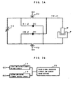
- the DC power source is divided between a DC power source (main DC power source) for applying the discharge current and a DC power source for energy regeneration, the voltage value V of the main DC power source being fixed to be constant, and the voltage value of the DC power source for energy regeneration being adjustable (i.e., the value of t2 being adjustable), in order to solve this problem.
- a DC power source main DC power source
- a DC power source for energy regeneration adjustable (i.e., the value of t2 being adjustable), in order to solve this problem.
- first and second switching elements T11 and T12 When both first and second switching elements T11 and T12 are turned on, a voltage V of a main DC power source 10 is applied between a workpiece W and an electrode P, and a discharge current J0 flows there. When both the first and second switching elements T11 and T12 are turned off a current J1 produced by induced energy that is accumulated by inductance in the circuit of FIG. 12 returns to a power source 20 for energy regeneration through a first diode D11, the workpiece W, the machining electrode P, and a second diode D12.
- a current peak value Jp is determined by a pulse width with which both the first and second switching elements T11 and T12 are turned on, that is, a current peak value setting pulse width t1.
- a fall time t2 of the current is determined by the voltage of the DC power source 20 for regeneration. This time t2 can be adjusted by regulating the voltage of the DC power source 20 for regeneration. In consequence, a machining pulse width (t1 + t2) can be selected by regulating the voltage of the DC power source 20 for regeneration.
- FIG. 13 is a diagram showing current waveforms and the like for the case where the voltage of the DC power source 20 for regeneration is raised in the electric discharge machining power source circuit shown in FIG. 12.
- FIG. 14 is a diagram showing current waveforms and the like for the case where the voltage of the DC power source 20 for regeneration is lowered.
- the current peak value Jp is determined by the current peak value setting pulse width t1 with which the switching elements T11 and T12 are turned on and the voltage (constant) of the main DC power source. Thus, if the current peak value setting pulse width t1 is common to both cases of FIGS. 13 and 14, therefore, the current peak value Jp is also a common value.
- the discharge current waveforms are triangular, thus constituting a substantial hindrance to the improvement of the electric discharge machining characteristics.
- Electric discharge in electric discharge machining starts with finding out an infinitesimal conduction path of scores of micrometers or less in a gap between the electrode and the workpiece, then supplying a pulse current there, and forcing the infinitesimal conduction path or infinitesimal portions of the electrode and the workpiece in contact with it to transpire or fuse and scatter by means of heat energy produced there.
- the degree of the transpiration or fusional scattering in the infinitesimal portions is determined by the level of the rate of change in the pulse current with respect to time, that is, the levels of the current having a sharp leading edge and the current peak value, the thermal properties of the electrode, workpiece material, etc., the cooling properties of an insulating solution, and the like.
- the workpiece is formed of a material with low electric resistance, heat generation attributable to Joule heat is low. If it is formed of a material with high thermal conductivity, heat generation or temperature rise in the infinitesimal portions can be restrained. Further, a material with substantial fusion latent heat and high fusion temperature cannot easily fuse if it is heated. A material that is highly viscous when it is fused is not ready to scatter if it is fused.
- Wire electrodes for wire electric discharge machining include special wires that are coated with a material having low fusion temperature and low fused-state viscosity. They have an effect to prevent the aforesaid short-circuiting, thereby improving the machining efficiency.
- each of various conditions including the discharge time (pulse width) as machinability, as well as the levels of the current peak value and the current rise speed as electric discharge starting capability, can be selected independently of one another, according to differences in an electrode, a workpiece, and a themal property of insulating solution.
- discharge time pulse width
- levels of the current peak value and the current rise speed as electric discharge starting capability can be selected independently of one another, according to differences in an electrode, a workpiece, and a themal property of insulating solution.
- the object of the present invention is to provide an electric discharge machining power source unit for an electric discharge machine, capable of obtaining electric discharge machining current pulses that rise and fall sharply and ensure satisfactory machining efficiency.
- an electric discharge machining power source unit comprises: a first DC power source; a second DC power source designed for an output voltage lower than that of the first DC power source; a pulse generator circuit for respectively outputting first pulses having a set first width and second pulses having a set second width at time intervals; a first circuit for applying a voltage from the first DC power source between a machining electrode and a workpiece while the first pulses are being outputted; a second circuit for applying a voltage from the second DC power source between the machining electrode and the workpiece while the second pulses are being outputted; and a third circuit adapted to feed back a current produced by induced energy accumulated by inductance in the second circuit to the first DC power source when the delivery of the first pulses is stopped and the delivery of the second pulses is stopped thereafter.
- the peak value of an electric discharge machining current and the machining pulse width can be set with ease, and an electric discharge machining current having a substantially square waveform can be obtained that rises and falls sharply in a short time, so that the electric discharge machining efficiency can be improved. Since the machining current having a sharp and narrow square waveform can be obtained, hard metal materials, such as tungsten carbide, and electrically conductive ceramics that are liable to thermal-shock cracks can be machined with high efficiency. A wire electric discharge machine can be remarkably improved in machining speed compared to work surface roughness, in particular.
- the positive terminal of a main DC power source 1 is connected to a workpiece W through a first switching element T1, while the negative terminal thereof is connected to a machining electrode P through a second switching element T2. Further, the positive terminal of an auxiliary DC power source 2 is connected to the workpiece W through a third switching element T3, while the negative terminal thereof is connected to the negative terminal of the main DC power source 1.
- a first diode D1 is reversely connected between the negative terminal of the main DC power source 1 (and the auxiliary DC power source 2) and the workpiece W.
- a second diode D2 is reversely connected between the positive terminal of the main DC power source 1 and the machining electrode P.
- the workpiece W and the machining electrode P are connected to the positive and negative sides, respectively, of the main DC power source 1. In some cases, however, the workpiece W and the machining electrode P may be connected contrariwise, that is, to the negative and positive sides, respectively, of the main DC power source 1.
- the first, second, and third switching elements T1, T2 and T3 are formed of a transistor or FET each. In the present embodiment, they are formed of an FET each. As shown in FIG. 1B, first, second, and third switching element driver circuits 6, 7 and 8 are connected, respectively, to gates G1, G2 and G3 of the FETs that individually constitute the switching elements T1, T2 and T3.
- the first, second, and third switching element driver circuits 6, 7 and 8 are designed to turn on and off the first, second, and third switching elements T1, T2 and T3, respectively, in response to pulses delivered from a pulse distribution circuit 5.
- the pulse distribution circuits 5 is formed of a monostable multivibrator or the like.
- the pulse distribution circuit 5 outputs pulses with pulse widths previously determined in accordance with current peak value setting data (t1) and pulse width setting data (t2) delivered from a controller 3 for controlling an electric discharge machine, in response to timing signals delivered from an electric discharge timing generator circuit 4, thereby turning on the first, second, and third switching elements T1, T2 and T3, as mentioned later.
- the electric discharge timing generator circuit 4 (a detection circuit of which is not shown) detects electric discharge or conduction between the workpiece W and the machining electrode P, and outputs the timing signals in accordance with conditions for electric discharge between the machining electrode P and the workpiece W.
- FIG. 4 shows the operation timing and discharge current (machining current) waveforms for the electric discharge machining power source unit according to the first embodiment.
- the pulse distribution circuit 5 When a timing signal is delivered from the electric discharge timing generator circuit 4 in accordance with the conditions for electric discharge between the machining electrode P and the workpiece W, the pulse distribution circuit 5 first outputs a pulse with a time width t2 that is previously set in accordance with the pulse width setting data, and causes the second and third switching element driver circuits 7 and 8 to turn on the second and third switching elements T2 and T3 ((b) and (c) of FIG. 4).
- a pulse with a time width t1 set in accordance with the current peak value setting data is delivered from the pulse distribution circuit 5 ((a) of FIG. 4), whereupon the first switching element driver circuit 6 is caused to turn on the first switching element T1.
- high voltage from the main DC power source 1 is applied between the workpiece W and the machining electrode P through the first switching element and the second switching element T2, and the current J0 starts to flow from the main DC power source 1, whereupon the machining current J0 between the workpiece W and the machining electrode P sharply rises, as indicated by (d) of FIG. 4.
- the machining pulse width can be substantially determined by the pulse width setting data (t2) for turning on the second and third switching elements T2 and T3, as indicated by (d) of FIG. 4. Further, a peak value JP of the current can be determined by the current peak value setting data (t1) for turning on the first switching element T1.
- the current peak value and the machining pulse width can be determined independently of each other, so that these values can be set with ease. Since the rise and fall of the machining current can be sharpened by utilizing a main DC power source of high voltage, moreover, a substantially square machining current waveform can be obtained, so that the machining efficiency can be improved.
- the first switching element T1 is turned on after the passage of a short time since the second and third switching elements T2 and T3 are turned on.
- the first switching element T1 may be turned on at the same time when, or even before, the second and third switching elements T2 and T3 are turned on.
- the time for the start of activation of the first switching element T1 can only be adjusted for a lag or lead with respect to the time for the start of activation of the second and third switching elements T2 and T3, according to the material of the workpiece W and the like.
- FIGS. 2A, 2B and 5 there will be described the construction and operation of an electric discharge machining power source unit according to a second embodiment of the present invention.
- the electric discharge machining power source unit according to this second embodiment is equivalent to a modified version of the electric discharge machining power source unit according to the first embodiment (FIGS. 1A and 1B), in which a (third) diode D3 is used in place of the third switching element T3, and the third switching element driver circuit 8 is removed to match the modification.
- the pulse distribution circuit 6 When a timing signal is delivered from the electric discharge timing generator circuit 4, the pulse distribution circuit 6 first outputs a pulse with a time width t2 that is set in accordance with the pulse width setting data (t2), and causes the second switching element driver circuit 7 to turn on the second switching element T2, as indicated by ((b) of FIG. 5.
- a pulse with a time width t1 set in accordance with the current peak value setting data (t1) is delivered from the pulse distribution circuit 5 with a certain set time delay ((a) of FIG. 5), whereupon the first switching element driver circuit 6 is caused to turn on the first switching element T1.
- high voltage from the main DC power source 1 is applied between the workpiece W and the machining electrode P through the first switching element T1 and the second switching element T2, and the current J0 starts to flow from the main DC power source 1, whereupon the machining current J0 between the workpiece W and the machining electrode P sharply rises, as indicated by (c) of FIG. 5.
- the machining pulse width can be substantially determined by the pulse width setting data (t2), as indicated by (c) of FIG. 5. Further, a peak value JP of the current can be determined by the current peak value setting data (t1) for turning on the first switching element T1.
- the current peak value JP and the machining pulse width can be determined independently of each other, so that these values can be set with ease. Since the rise and fall of the machining current can be sharpened by utilizing a main DC power source of high voltage, moreover, a substantially square machining current waveform can be obtained, so that the machining efficiency can be improved.
- FIGS. 3A, 3B and 6 there will be described the construction and operation of an electric discharge machining power source unit according to a third embodiment of the present invention.
- the electric discharge machining power source unit according to the third embodiment differs from the electric discharge machining power source unit according to the second embodiment described above in that the main DC power source 1 and the auxiliary DC power source 2 are connected in series with each other. More specifically, the positive terminal of the auxiliary DC power source 2 is connected to the negative terminal of the main DC power source 1, the positive terminal of the main DC power source 1 is connected to the workpiece W through the first switching element T1, and the negative terminal of the auxiliary DC power source 2 is connected to the machining electrode P through the second switching element T2.
- the first diode D1 is connected in the forward direction between the workpiece W and a connection point between the auxiliary DC power source 2 and the main DC power source 1, while the second diode D2 is connected in the reverse direction between the positive terminal of the main DC power source 1 and the machining electrode P.
- the first and second switching elements T1 and T2 are formed of an FET each. Their respective gates G1 and G2 are driven by means of the circuit shown in FIG. 3B. Since a circuit (FIG. 3B) for controlling the first and second switching elements shown in FIG. 3A is identical with that shown in FIG. 2B, a description of the circuit is omitted.
- the pulse distribution circuit 5 When a timing signal is delivered from the electric discharge timing generator circuit 4, the pulse distribution circuit 5 first outputs a pulse with a pulse width t2 that is set in accordance with the pulse width setting data (t2), and causes the second switching element driver circuit 7 to turn on the second switching element T2, as indicated by ((b) of FIG. 6.
- a current J0 flows from the auxiliary DC power source 2 to the workpiece W, machining electrode P, second switching element T2, and auxiliary DC power source 2 through the first diode D1, whereupon conduction points are secured ((c) and (d) of FIG. 6). Since the output voltage of the auxiliary DC power source 2 is low, this current rises gently.
- a pulse with a time width t1 set in accordance with the current peak value setting data is delivered from the pulse distribution circuit 5 with a set delay time ((a) of FIG. 5), whereupon the first switching element driver circuit 6 is caused to turn on the first switching element T1 ((a) of FIG. 6).
- current starts to flow from the high-voltage main DC power source 1, whereupon the machining current J0 between the workpiece W and the machining electrode P sharply rises, as indicated by (c) of FIG. 5.
- a third switching element may be provided in place of the first diode D1. Since the first diode D1 constitutes a part of the circuit for feeding back the induced energy to the main DC power source 1, in this case, it is necessary only that a diode be connected in the reverse direction between the negative terminal of the auxiliary DC power source 2 and the workpiece W in order to feed back the induced energy. As in the case of the first embodiment, the third switching element must only be turned on or off at the same time with the second switching element T2.
- the machining pulse width can be substantially determined by the pulse width setting data (t2), as indicated by (c) of FIG. 6. Further, a peak value JP of the current can be determined by the current peak value setting data (t1) for turning on the first switching element T1.
- the current peak value JP and the machining pulse width can be determined independently of each other, so that these values can be set with ease. Since the rise and fall of the machining current can be sharpened by utilizing the high main DC power source voltage, moreover, a substantially square machining current waveform can be obtained, so that the machining efficiency can be improved.
- TABLE 1 is a table showing the respective performances of the electric discharge machining power source unit according to the present invention and the conventional electric discharge machining power source unit, compared by carrying out wire electric discharge machining using SKD11 for the material of the workpiece W and a brass wire of 0.2-mm diameter as the wire machining electrode P.
- TABLE 2 is a performance comparison table prepared by carrying out wire electric discharge machining using the electric discharge machining power source unit according to the present invention with the current peak value kept constant (at 210 A) and with the machining pulse width varied.
Landscapes
- Engineering & Computer Science (AREA)
- Mechanical Engineering (AREA)
- Electrical Discharge Machining, Electrochemical Machining, And Combined Machining (AREA)
Applications Claiming Priority (3)
| Application Number | Priority Date | Filing Date | Title |
|---|---|---|---|
| JP22701297 | 1997-08-11 | ||
| JP22701297A JP3347277B2 (ja) | 1997-08-11 | 1997-08-11 | 放電加工機の放電加工電源装置 |
| PCT/JP1998/003574 WO1999007510A1 (fr) | 1997-08-11 | 1998-08-11 | Systeme d'alimentation electrique pour ensembles d'usinage par etincelle |
Publications (3)
| Publication Number | Publication Date |
|---|---|
| EP0943387A1 true EP0943387A1 (fr) | 1999-09-22 |
| EP0943387A4 EP0943387A4 (fr) | 2004-08-18 |
| EP0943387B1 EP0943387B1 (fr) | 2006-05-31 |
Family
ID=16854140
Family Applications (1)
| Application Number | Title | Priority Date | Filing Date |
|---|---|---|---|
| EP98936739A Expired - Lifetime EP0943387B1 (fr) | 1997-08-11 | 1998-08-11 | Systeme d'alimentation electrique pour ensembles d'usinage par etincelle |
Country Status (4)
| Country | Link |
|---|---|
| US (1) | US6130510A (fr) |
| EP (1) | EP0943387B1 (fr) |
| JP (1) | JP3347277B2 (fr) |
| WO (1) | WO1999007510A1 (fr) |
Families Citing this family (19)
| Publication number | Priority date | Publication date | Assignee | Title |
|---|---|---|---|---|
| WO2001051240A1 (fr) * | 2000-01-11 | 2001-07-19 | Mitsubishi Denki Kabushiki Kaisha | Alimentation electrique pour traitement de surface de decharge et procede de traitement de surface de decharge |
| WO2001094067A1 (fr) * | 2000-06-06 | 2001-12-13 | Mitsubishi Denki Kabushiki Kaisha | Alimentation electrique pour usinage par etincelage |
| JP4152080B2 (ja) | 2000-12-01 | 2008-09-17 | 三菱電機株式会社 | 放電加工装置 |
| WO2003089175A1 (fr) | 2002-04-22 | 2003-10-30 | Mitsubishi Denki Kabushiki Kaisha | Alimentation electrique d'usinage d'une machine d'usinage a decharge electrique par fil |
| ATE356686T1 (de) * | 2002-06-03 | 2007-04-15 | Charmilles Technologies | Funkenerosionsmaschine |
| CN100345651C (zh) | 2002-07-12 | 2007-10-31 | 三菱电机株式会社 | 放电加工用电源装置 |
| US8248750B2 (en) | 2007-12-13 | 2012-08-21 | Bayer Materialscience Ag | Electroactive polymer transducers |
| JP5896591B2 (ja) * | 2006-12-14 | 2016-03-30 | パーカー ハネフィン コーポレイションParker Hannifin Corporation | 容量性構造体、その製造方法およびその作動方法ならびに容量性構造体を備えたシステム |
| US7952261B2 (en) | 2007-06-29 | 2011-05-31 | Bayer Materialscience Ag | Electroactive polymer transducers for sensory feedback applications |
| JP5442962B2 (ja) * | 2008-06-16 | 2014-03-19 | 三菱電機株式会社 | 放電加工方法 |
| EP2239793A1 (fr) | 2009-04-11 | 2010-10-13 | Bayer MaterialScience AG | Montage de film polymère électrique commutable et son utilisation |
| JP5088975B2 (ja) * | 2010-10-19 | 2012-12-05 | 株式会社ソディック | ワイヤ放電加工装置 |
| WO2012118916A2 (fr) | 2011-03-01 | 2012-09-07 | Bayer Materialscience Ag | Procédés de fabrication automatisés pour la production de dispositifs et de films polymères déformables |
| JP2014517331A (ja) | 2011-03-22 | 2014-07-17 | バイエル・インテレクチュアル・プロパティ・ゲゼルシャフト・ミット・ベシュレンクテル・ハフツング | 電場応答性高分子アクチュエータレンチキュラシステム |
| JP5192570B2 (ja) * | 2011-07-14 | 2013-05-08 | ファナック株式会社 | ワイヤ電極の消耗を抑えるワイヤ放電加工機の放電加工電源装置 |
| US9876160B2 (en) | 2012-03-21 | 2018-01-23 | Parker-Hannifin Corporation | Roll-to-roll manufacturing processes for producing self-healing electroactive polymer devices |
| KR20150031285A (ko) | 2012-06-18 | 2015-03-23 | 바이엘 인텔렉쳐 프로퍼티 게엠베하 | 연신 공정을 위한 연신 프레임 |
| JP5778650B2 (ja) | 2012-10-11 | 2015-09-16 | ファナック株式会社 | ワイヤ放電加工機およびワイヤ放電加工方法 |
| US9590193B2 (en) | 2012-10-24 | 2017-03-07 | Parker-Hannifin Corporation | Polymer diode |
Family Cites Families (12)
| Publication number | Priority date | Publication date | Assignee | Title |
|---|---|---|---|---|
| US3120619A (en) * | 1961-04-13 | 1964-02-04 | Elox Corp Michigan | Transistorized electric discharge machining circuit |
| US4004123A (en) * | 1973-02-20 | 1977-01-18 | Inoue K | Method of and system for the controlling of an apparatus for the electric discharge machining of a workpiece |
| JPS62287911A (ja) * | 1986-06-06 | 1987-12-14 | Mitsubishi Electric Corp | 放電加工用電源装置 |
| JP2767892B2 (ja) * | 1989-05-30 | 1998-06-18 | ブラザー工業株式会社 | 放電加工機用電源 |
| JPH0761568B2 (ja) * | 1989-08-08 | 1995-07-05 | 三菱電機株式会社 | 放電加工装置の波形制御装置 |
| JP2939310B2 (ja) * | 1990-08-14 | 1999-08-25 | 株式会社ソディック | 放電加工装置 |
| US5306889A (en) * | 1991-07-05 | 1994-04-26 | Sodick Co., Ltd. | Wire cut electrical discharge machining apparatus |
| JP2914102B2 (ja) * | 1993-06-30 | 1999-06-28 | 三菱電機株式会社 | 放電加工機 |
| JPH07290317A (ja) * | 1994-04-25 | 1995-11-07 | Fanuc Ltd | 放電加工方法及びその装置 |
| JP2983139B2 (ja) * | 1994-04-26 | 1999-11-29 | 株式会社ソディック | 放電加工用電源回路及び放電加工装置 |
| JP3245087B2 (ja) * | 1997-05-12 | 2002-01-07 | 三菱電機株式会社 | 放電加工装置用電源装置 |
| US5872347A (en) * | 1997-06-24 | 1999-02-16 | Industrial Technology Research Institute | Method and device for controlling discharging current slope of wire cut electrical discharge machine |
-
1997
- 1997-08-11 JP JP22701297A patent/JP3347277B2/ja not_active Expired - Lifetime
-
1998
- 1998-08-11 WO PCT/JP1998/003574 patent/WO1999007510A1/fr not_active Ceased
- 1998-08-11 US US09/284,280 patent/US6130510A/en not_active Expired - Lifetime
- 1998-08-11 EP EP98936739A patent/EP0943387B1/fr not_active Expired - Lifetime
Also Published As
| Publication number | Publication date |
|---|---|
| WO1999007510A1 (fr) | 1999-02-18 |
| JP3347277B2 (ja) | 2002-11-20 |
| JPH1148039A (ja) | 1999-02-23 |
| EP0943387B1 (fr) | 2006-05-31 |
| EP0943387A4 (fr) | 2004-08-18 |
| US6130510A (en) | 2000-10-10 |
Similar Documents
| Publication | Publication Date | Title |
|---|---|---|
| US6130510A (en) | Electric discharge machining power source unit for electric discharge machine | |
| JPS6116571B2 (fr) | ||
| US9719479B2 (en) | Ignition control device for internal combustion engine | |
| CN103958103A (zh) | 放电加工机用电源装置 | |
| TW504422B (en) | Power supply device for a discharge machine | |
| JPH0761568B2 (ja) | 放電加工装置の波形制御装置 | |
| JPWO2001087526A1 (ja) | 放電加工用電源装置 | |
| US7582842B2 (en) | Method and apparatus for generating machining pulses for electrical discharge machining | |
| JPH0521689B2 (fr) | ||
| JP2652392B2 (ja) | 放電加工電源 | |
| US5345053A (en) | Method and apparatus for supplying power for electric discharge machining | |
| US5378866A (en) | Electric discharge machining system having a secondary power supply including a controllable voltage source and impedance | |
| US11420277B2 (en) | Wire electrical discharge machine and control method of wire electrical discharge machine | |
| US6630641B2 (en) | Electric discharge machining apparatus generating preliminary discharge and machining discharge pulses | |
| JPH062310B2 (ja) | パルスア−ク溶接方法 | |
| JP5013392B2 (ja) | ワイヤ放電加工機の加工電源装置 | |
| US6211481B1 (en) | Power supply device for electric discharge machining apparatus | |
| TW458831B (en) | Power supply apparatus for electrodischarge machine and electrodischarge machining method | |
| JP2801280B2 (ja) | ワイヤカット放電加工電源 | |
| JPH11333632A (ja) | 放電加工装置 | |
| TWI839195B (zh) | 線切割粗加工電波形調變方法 | |
| JP2918748B2 (ja) | 放電加工方法及び装置 | |
| TWI860084B (zh) | 雙電阻電容放電加工系統 | |
| JPH05152653A (ja) | レーザ励起用ランプの電源装置 | |
| JP2008524564A (ja) | 導波管に電流パルスを発生するための回路および方法 |
Legal Events
| Date | Code | Title | Description |
|---|---|---|---|
| PUAI | Public reference made under article 153(3) epc to a published international application that has entered the european phase |
Free format text: ORIGINAL CODE: 0009012 |
|
| 17P | Request for examination filed |
Effective date: 19990504 |
|
| AK | Designated contracting states |
Kind code of ref document: A1 Designated state(s): CH LI |
|
| RAP1 | Party data changed (applicant data changed or rights of an application transferred) |
Owner name: FANUC LTD |
|
| A4 | Supplementary search report drawn up and despatched |
Effective date: 20040705 |
|
| 17Q | First examination report despatched |
Effective date: 20050201 |
|
| GRAP | Despatch of communication of intention to grant a patent |
Free format text: ORIGINAL CODE: EPIDOSNIGR1 |
|
| GRAS | Grant fee paid |
Free format text: ORIGINAL CODE: EPIDOSNIGR3 |
|
| GRAA | (expected) grant |
Free format text: ORIGINAL CODE: 0009210 |
|
| AK | Designated contracting states |
Kind code of ref document: B1 Designated state(s): CH LI |
|
| REG | Reference to a national code |
Ref country code: CH Ref legal event code: EP |
|
| REG | Reference to a national code |
Ref country code: CH Ref legal event code: NV Representative=s name: R. A. EGLI & CO. PATENTANWAELTE |
|
| PLBE | No opposition filed within time limit |
Free format text: ORIGINAL CODE: 0009261 |
|
| STAA | Information on the status of an ep patent application or granted ep patent |
Free format text: STATUS: NO OPPOSITION FILED WITHIN TIME LIMIT |
|
| 26N | No opposition filed |
Effective date: 20070301 |
|
| PGFP | Annual fee paid to national office [announced via postgrant information from national office to epo] |
Ref country code: CH Payment date: 20080912 Year of fee payment: 11 |
|
| REG | Reference to a national code |
Ref country code: CH Ref legal event code: PL |
|
| PG25 | Lapsed in a contracting state [announced via postgrant information from national office to epo] |
Ref country code: LI Free format text: LAPSE BECAUSE OF NON-PAYMENT OF DUE FEES Effective date: 20090831 Ref country code: CH Free format text: LAPSE BECAUSE OF NON-PAYMENT OF DUE FEES Effective date: 20090831 |