EP0943438A1 - Tintenstrahlkopf für anschlagfreien Drucker - Google Patents
Tintenstrahlkopf für anschlagfreien Drucker Download PDFInfo
- Publication number
- EP0943438A1 EP0943438A1 EP99104752A EP99104752A EP0943438A1 EP 0943438 A1 EP0943438 A1 EP 0943438A1 EP 99104752 A EP99104752 A EP 99104752A EP 99104752 A EP99104752 A EP 99104752A EP 0943438 A1 EP0943438 A1 EP 0943438A1
- Authority
- EP
- European Patent Office
- Prior art keywords
- ink jet
- piezoelectric element
- jet head
- circuit substrate
- head according
- Prior art date
- Legal status (The legal status is an assumption and is not a legal conclusion. Google has not performed a legal analysis and makes no representation as to the accuracy of the status listed.)
- Granted
Links
- 239000000758 substrate Substances 0.000 claims abstract description 81
- 229910000679 solder Inorganic materials 0.000 claims description 8
- 239000002245 particle Substances 0.000 claims description 6
- 230000002787 reinforcement Effects 0.000 claims description 6
- OKTJSMMVPCPJKN-UHFFFAOYSA-N Carbon Chemical compound [C] OKTJSMMVPCPJKN-UHFFFAOYSA-N 0.000 claims description 3
- 229920000049 Carbon (fiber) Polymers 0.000 claims description 3
- 229910001111 Fine metal Inorganic materials 0.000 claims description 3
- 229910052799 carbon Inorganic materials 0.000 claims description 3
- 239000004917 carbon fiber Substances 0.000 claims description 3
- 229910052802 copper Inorganic materials 0.000 claims description 3
- 229920001971 elastomer Polymers 0.000 claims description 3
- 239000002923 metal particle Substances 0.000 claims description 3
- 229920002379 silicone rubber Polymers 0.000 claims description 3
- 239000004945 silicone rubber Substances 0.000 claims description 3
- 229910052737 gold Inorganic materials 0.000 claims description 2
- 230000004044 response Effects 0.000 claims description 2
- 230000010355 oscillation Effects 0.000 abstract description 8
- 230000009467 reduction Effects 0.000 description 11
- 238000007639 printing Methods 0.000 description 10
- 239000004020 conductor Substances 0.000 description 8
- 238000000034 method Methods 0.000 description 8
- 238000010276 construction Methods 0.000 description 5
- 238000005549 size reduction Methods 0.000 description 5
- 239000000463 material Substances 0.000 description 4
- 239000002365 multiple layer Substances 0.000 description 4
- 239000002356 single layer Substances 0.000 description 4
- 239000012790 adhesive layer Substances 0.000 description 3
- 239000010410 layer Substances 0.000 description 3
- 239000000853 adhesive Substances 0.000 description 2
- 230000001070 adhesive effect Effects 0.000 description 2
- 230000000694 effects Effects 0.000 description 2
- 230000006872 improvement Effects 0.000 description 2
- 238000004544 sputter deposition Methods 0.000 description 2
- 230000002542 deteriorative effect Effects 0.000 description 1
- 239000003822 epoxy resin Substances 0.000 description 1
- 238000005530 etching Methods 0.000 description 1
- 230000004907 flux Effects 0.000 description 1
- 239000003365 glass fiber Substances 0.000 description 1
- 238000004519 manufacturing process Methods 0.000 description 1
- 230000000873 masking effect Effects 0.000 description 1
- 239000002184 metal Substances 0.000 description 1
- 229910052751 metal Inorganic materials 0.000 description 1
- 238000012986 modification Methods 0.000 description 1
- 230000004048 modification Effects 0.000 description 1
- 239000004033 plastic Substances 0.000 description 1
- 229920000647 polyepoxide Polymers 0.000 description 1
- 230000002265 prevention Effects 0.000 description 1
- 229920005989 resin Polymers 0.000 description 1
- 239000011347 resin Substances 0.000 description 1
- 238000007650 screen-printing Methods 0.000 description 1
Images


Classifications
-
- B—PERFORMING OPERATIONS; TRANSPORTING
- B41—PRINTING; LINING MACHINES; TYPEWRITERS; STAMPS
- B41J—TYPEWRITERS; SELECTIVE PRINTING MECHANISMS, i.e. MECHANISMS PRINTING OTHERWISE THAN FROM A FORME; CORRECTION OF TYPOGRAPHICAL ERRORS
- B41J2/00—Typewriters or selective printing mechanisms characterised by the printing or marking process for which they are designed
- B41J2/005—Typewriters or selective printing mechanisms characterised by the printing or marking process for which they are designed characterised by bringing liquid or particles selectively into contact with a printing material
- B41J2/01—Ink jet
- B41J2/135—Nozzles
- B41J2/16—Production of nozzles
- B41J2/1621—Manufacturing processes
- B41J2/1623—Manufacturing processes bonding and adhesion
-
- B—PERFORMING OPERATIONS; TRANSPORTING
- B41—PRINTING; LINING MACHINES; TYPEWRITERS; STAMPS
- B41J—TYPEWRITERS; SELECTIVE PRINTING MECHANISMS, i.e. MECHANISMS PRINTING OTHERWISE THAN FROM A FORME; CORRECTION OF TYPOGRAPHICAL ERRORS
- B41J2/00—Typewriters or selective printing mechanisms characterised by the printing or marking process for which they are designed
- B41J2/005—Typewriters or selective printing mechanisms characterised by the printing or marking process for which they are designed characterised by bringing liquid or particles selectively into contact with a printing material
- B41J2/01—Ink jet
- B41J2/135—Nozzles
- B41J2/14—Structure thereof only for on-demand ink jet heads
- B41J2/14201—Structure of print heads with piezoelectric elements
- B41J2/14274—Structure of print heads with piezoelectric elements of stacked structure type, deformed by compression/extension and disposed on a diaphragm
-
- B—PERFORMING OPERATIONS; TRANSPORTING
- B41—PRINTING; LINING MACHINES; TYPEWRITERS; STAMPS
- B41J—TYPEWRITERS; SELECTIVE PRINTING MECHANISMS, i.e. MECHANISMS PRINTING OTHERWISE THAN FROM A FORME; CORRECTION OF TYPOGRAPHICAL ERRORS
- B41J2/00—Typewriters or selective printing mechanisms characterised by the printing or marking process for which they are designed
- B41J2/005—Typewriters or selective printing mechanisms characterised by the printing or marking process for which they are designed characterised by bringing liquid or particles selectively into contact with a printing material
- B41J2/01—Ink jet
- B41J2/135—Nozzles
- B41J2/16—Production of nozzles
- B41J2/1607—Production of print heads with piezoelectric elements
- B41J2/1612—Production of print heads with piezoelectric elements of stacked structure type, deformed by compression/extension and disposed on a diaphragm
-
- B—PERFORMING OPERATIONS; TRANSPORTING
- B41—PRINTING; LINING MACHINES; TYPEWRITERS; STAMPS
- B41J—TYPEWRITERS; SELECTIVE PRINTING MECHANISMS, i.e. MECHANISMS PRINTING OTHERWISE THAN FROM A FORME; CORRECTION OF TYPOGRAPHICAL ERRORS
- B41J2/00—Typewriters or selective printing mechanisms characterised by the printing or marking process for which they are designed
- B41J2/005—Typewriters or selective printing mechanisms characterised by the printing or marking process for which they are designed characterised by bringing liquid or particles selectively into contact with a printing material
- B41J2/01—Ink jet
- B41J2/135—Nozzles
- B41J2/14—Structure thereof only for on-demand ink jet heads
- B41J2002/14387—Front shooter
-
- B—PERFORMING OPERATIONS; TRANSPORTING
- B41—PRINTING; LINING MACHINES; TYPEWRITERS; STAMPS
- B41J—TYPEWRITERS; SELECTIVE PRINTING MECHANISMS, i.e. MECHANISMS PRINTING OTHERWISE THAN FROM A FORME; CORRECTION OF TYPOGRAPHICAL ERRORS
- B41J2/00—Typewriters or selective printing mechanisms characterised by the printing or marking process for which they are designed
- B41J2/005—Typewriters or selective printing mechanisms characterised by the printing or marking process for which they are designed characterised by bringing liquid or particles selectively into contact with a printing material
- B41J2/01—Ink jet
- B41J2/135—Nozzles
- B41J2/14—Structure thereof only for on-demand ink jet heads
- B41J2002/14491—Electrical connection
Definitions
- the present invention relates to ink jet heads for non-impact printers, in which ink is jet from a nozzle for printing.
- printers are finding various applications. These printers are in dependence on the type of printing classified into impact printers for impact printing and non-impact printers for non-impact printing.
- the non-impact printers are capable of low noise, high resolution and relatively high speed printing.
- These printers include ink jet printers and are finding extensive applications.
- a prior art ink jet printer adopts an ink jet head as shown in Fig. 5, for instance.
- the illustrated ink jet head 51 comprises a laminate piezoelectric element 52 and a circuit substrate 53.
- the laminate piezoelectric element 52 has inner and outer electrodes 54 and 55 in conductive connection with one another. Oscillations of the laminate piezoelectric element 52 are transmitted via an adhesive layer 58 and an oscillating plate 59 to a pressure chamber 57 communicated with an ink jet nozzle 56.
- the pressure chamber 57 is formed by the oscillating plate 59 and a nozzle plate 60.
- the circuit substrate 53 is connected to the laminate piezoelectric element 52 via a flexible printed circuit board or lead members 61 such as wires.
- the circuit substrate 53 is formed with a driver IC (not shown) for driving the laminate piezoelectric element 52, and connectors 62 for connecting the laminate piezoelectric element 52 are mounted on the circuit substrate 53.
- a drive signal is thus supplied from the driver IC (not shown)of the circuit substrate 53 to the laminate piezoelectric element 52.
- the circuit substrate 53 is formed with a conductive pattern (not shown), which connects the connectors 60 and the drive IC (not shown) to one another.
- a drive signal supplied from the circuit substrate 53 to the laminate piezoelectric element 52 generates oscillations thereof, and the oscillations thus generated are transmitted via the adhesive layer 58 and the oscillating plate 59 to the pressure chamber 57 to cause jetting of ink from the nozzle 56.
- this prior art ink jet head uses the lead members 61 for the connection of the laminate piezoelectric element 52 and the circuit substrate 53 to each other, noise that is introduced increases the possibility of erroneous head operation, thus deteriorating the qualitative reliability.
- the erroneous head operation possibility due to noise introduction is increased by an increased number of lead members 61.
- each laminate piezoelectric element 52 and the circuit substrate 53 should be spaced apart by a certain distance. This distance causes the characteristic impedance increase and the induced voltage applied increase to the drive IC.
- the induced voltage increase does not only result in inter-drive signal crosstalk increase, waveform dulling and ringing to cause erroneous head operation, but also result in the destroy or routine of the drive IC.
- the increase of the number of the lead members 61 increases the number of times of connection of the lead members 61. Therefore, the operability of connection of the laminate piezoelectric elements 52 to the circuit substrate 53 is correspondingly deteriorated to reduce the yield.
- the lead members 61 are used for electrically connecting the circuit substrate 53 and the laminate piezoelectric element 52, retaining members (not shown) are separately required for mechanical connection, thus not only increasing the number of components and the number of operating steps but also complicating the operation of connecting the laminate piezoelectric element 52 and the circuit substrate 53 to each other and increasing the cost.
- the use of the wire members 61 has a further drawback that with increasing nozzle number the space for connection is increased and the size of the head as a whole is increased.
- Japanese Patent Disclosure No. 9-286111 shows a prior art entitled "Method of Manufacturing Ink Jet Head".
- piezoelectric elements on an ink head substrate and electrodes on plate-like lead member are bonded together by a conductive adhesive, which is poured via thorough holes formed in the lead member.
- the disclosed prior art features in forming through holes in the substrates.
- the least permissible hole diameter and land diameter of the thorough holes formed in the glass fiber epoxy resin substrate are 0.3 and 0.5 mm, respectively, in the case of the single-layer substrate and 0.3 and 0.7 mm, respectively, in the case of the multiple-layer substrate (the least permissible inter-land distance being 0.2 mm).
- the least permissible electrode pitch is 0.7 mm in the case of the single-layer substrate and 0.9 mm in the case of the multiple-layer substrate, that is, it is possible to obtain a resolution only up to 36 dpi per row in the case of the single-layer substrate and up to 28 dpi in the case of the multiple-layer substrate.
- the present invention was made in view of the above background, its object is to provide an ink jet head, in which electric bonding members are provided between a piezoelectric element for providing oscillations to a pressure chamber communicated with an ink jet nozzle and a circuit substrate having a head driving circuit, thus permitting improvement of the qualitative reliability and the yield, cost reduction, head size reduction, prevention of erroneous head operation and rupture of a driver IC (i.e., head driving circuit).
- a driver IC i.e., head driving circuit
- an ink jet head comprising a piezoelectric element having inner and outer electrodes in electric conduction to one another and for providing vibrations to a pressure chamber communicated with an ink jet nozzle, and a circuit substrate disposed near the piezoelectric element and having a head driving circuit, wherein:
- the piezoelectric element is a laminate piezoelectric element and the laminate piezoelectric head is constituted by a plurality of sub-elements.
- the outer electrodes are formed separately for each sub-element, and extend along side surfaces of the laminate piezoelectric element and the end thereof nearer the circuit substrate.
- circuit substrate and the piezoelectric element are connected to each other both electrically and mechanically at a time by the electric bonding members provided between them.
- the head driving circuit is formed on the circuit substrate on the side thereof opposite the piezoelectric element.
- drive signal from the head driving circuit is provided via the circuit substrate to the piezoelectric element.
- a reinforcement member is provided between the piezoelectric element and the circuit substrate.
- the mechanical strength of connection of the piezoelectric element and the circuit substrate to each other can be increased by the reinforcement member.
- the electric bonding members are constituted by bumps and the circuit substrate and the piezoelectric element are connected to each other both electrically and mechanically at a time by the bumps provided between them.
- the electric bonding members are constituted by an anisotropic conductive film.
- circuit substrate and the piezoelectric element are connected to each other both electrically and mechanically at a time by the anisotropic conductive film provided between them.
- the bump is solder, Au or Cu and the anisotropic conductive film is obtained by dispersedly burying carbon fibers, carbon particles, Au-plated metal particles, conductive rubber particles or fine metal wires in silicone rubber.
- an ink jet head comprising:
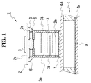
- Fig. 1 is a sectional view showing a first embodiment of the ink jet head according to the present invention.
- the illustrated ink jet head generally designated by reference numeral 1 comprises a circuit substrate 2, a piezoelectric element 3 and a pressure vessel 4.
- the circuit substrate 2 is a printed circuit board and disposed near the piezoelectric element 3.
- an ink jet head driver IC 5 is mounted, and connected to the conductor patterns 2a.
- the piezoelectric element 3 is a five-layer laminate piezoelectric element, and has inner and outer electrodes 3a and 3b in electric conduction to one another. Thus, when the piezoelectric element 3 is caused to oscillate, the oscillations are transmitted to a pressure vessel 4.
- the inner electrodes 3a of the piezoelectric element 3 are constituted by six electrodes including a common electrode.
- the outer electrodes 3b are constituted by two electrodes connected to corresponding ones of the inner electrodes 3a. Each outer electrode 3b extends toward the circuit substrate side along the side surface of the piezoelectric element 3.
- the piezoelectric element 3 is connected to the circuit substrate 2 via electric bonding members 6.
- the electric bonding members 6 are formed from a solder paste, and are formed by means of screen printing between the conductor patterns 2a and the outer electrodes 3b.
- the pressure vessel 4 has an oscillating plate 4a and a nozzle plate 4b, and is secured via an adhesive layer 7 to the piezoelectric element 3.
- the oscillating plate 4a is disposed on the piezoelectric element side.
- the nozzle plate 4b has an ink jet nozzle 8, and faces the oscillating plate 4a. Thus, when pressure variations are generated in the pressure vessel 4a, ink in the pressure vessel 4 is jet out therefrom through the nozzle 8.
- a reinforcement member 9 of an insulating plastic material is provided between the circuit substrate 2 and the piezoelectric element 3, and has an effect of increasing the mechanical strength of connection between the circuit substrate 2 and the piezoelectric element 3.
- the electric bonding member 6 provided between the circuit substrate 2 and the piezoelectric element 3 can suppress erroneous head operation due to noise introduction compared to the case of using lead members.
- the electric bonding members 6 provided between the circuit substrate 2 and the piezoelectric element 3 does not only permit the reduction of the space for connecting the circuit substrate 2 and the piezoelectric element 3 to each other, but also permit reduction of the induced voltage applied to the driver IC by reducing the characteristic impedance.
- circuit substrate 2 and the piezoelectric element 3 can be connected to each other both electrically and mechanically at a time.
- retaining members not shown which were heretofore necessary for the mechanical connection, thus permitting reduction of not only the number of components but also the number of operating steps.
- FIG. 2 is a perspective view showing the second embodiment of the ink jet head according to the present invention.
- the illustrated ink jet head generally designated by reference numeral 11 comprises a circuit substrate 12, a piezoelectric element 13 and a pressure vessel (not shown).
- the circuit substrate 12 is a printed circuit board and disposed above the piezoelectric element 13.
- an ink jet head driver IC 15 is mounted, and connected to the conductor patterns 12a.
- the conductor patterns 12a are of Au or like metal used as pattern material, and are provided by means of printing on the circuit substrate 12 on the piezoelectric element side thereof.
- the piezoelectric element 13 is a comb-like laminate piezoelectric element constituted by fine sub-elements 13A each of a five-layer laminate.
- Each sub-element 13A of the piezoelectric element 13 has inner and outer electrodes 13a and 13b in electric conduction to one another.
- the oscillations are transmitted to respective pressure vessels (not shown).
- the inner electrodes 13a of each sub-element are constituted by six electrodes including a common electrode, and are provided between adjacent ones of the laminated layers of the laminate piezoelectric element 13.
- the outer electrodes 13b of each sub-element are constituted by two electrodes connected to corresponding ones of the inner electrodes 13a.
- the outer electrodes 13b are formed by such means as a print baking method, a sputtering method using a masking and a method of etching after entire surface sputtering, such that they extend along the top and side surfaces of the piezoelectric element 13.
- the outer electrodes 13b are formed separately for each sub-element, such that each of them extend around a corner of the piezoelectric element 13 on the circuit substrate side thereof.
- the piezoelectric element 13 is connected via electric bonding members 16 to the circuit substrate 12 by, for instance, a re-flow method or a thermal press bonding method.
- the electric bonding members 16 consist of bumps of solder, Au or Cu, and are formed on the outer electrodes 13b or the conductor patterns 12a by, for instance a re-flow method.
- the electric bonding members 16 are formed by utilizing the viscosity of preliminary solder or flux applied to the outer electrodes 13b.
- a reinforcement member (not shown) of, for instance, an insulating resin is interposed between the circuit substrate 12 and the piezoelectric element 13, and has an effect of increasing the mechanical strength of connection of the circuit substrate 12 and the piezoelectric element 13 to each other.
- the ink jet head having the above construction like the first embodiment, it is possible to reduce the probability of erroneous head operation due to noise introduction, reduce the space for connecting the circuit substrate 12 and the piezoelectric element 13 to each other and reduce the induced voltage applied to the driver IC by reducing the characteristic impedance.
- the electric bonding members 16 may be provided by using solder bumps (or solder balls). Actually, balls to this end are mass produced down to a diameter of 0.1 mm. Using such balls, patterns 0.1 mm in width may be readily formed on the circuit substrate as in the prior art. It is thus possible to reduce the electrode pitch down to 0.2 mm and readily obtain a resolution of 127 dpi per row.
- an ink jet head capable of printing at 600 dpi per pass can be obtained by merely providing five piezoelectric element rows, and it is very readily possible to obtain size reduction of high resolution ink jet heads.
- solder balls are considerably inexpensive compared to conductive adhesives, it is possible to readily reduce the overall cost.
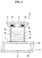
- Fig. 3 is a sectional view showing a third embodiment of the ink jet head according to the present invention.
- the illustrated ink jet head generally designated by reference numeral 21, like the first embodiment, comprises a circuit substrate 2, a piezoelectric element 3 and a pressure vessel 4.
- An electric bonding member 26 is provided between the outer electrodes 3b of the piezoelectric element 3 and the conductor patterns 12a of the circuit substrate 12 by a press bonding method or a thermal press bonding method.
- the electric bonding member 26 is in the form of an anisotropic conductive film of a material, which is obtained by dispersedly burying carbon fibers, carbon particles, Au-plated metal particles, conductive rubber particles or fine metal wires in, for instance, silicone rubber.
- ink jet head having the above construction like the first and second embodiments, it is possible to reduce the probability of erroneous head operation due to noise introduction and also reduce the space for connecting the circuit substrate 2 and the piezoelectric element 3.
- this embodiment it is possible to dispense with retaining members (not shown) which were heretofore necessary for mechanical connection, thus permitting reduction of not only the number of components but also the number of operating steps.
- the circuit substrate and the piezoelectric element are connected to each other via electric bonding members provided between them, and it is thus possible to reduce the probability of erroneous head operation due to noise introduction.
- the probability of erroneous head operation due to noise introduction may also be reduced in the case of a multiple nozzle structure, in which a number of piezoelectric elements are connected to the circuit substrate, thus obtaining qualitative reliability improvement.
- the space for connecting the circuit substrate and the piezoelectric element to each other can be reduced, thus permitting size reduction of the head as a whole.
- the electric bonding members provided between the circuit substrate and the piezoelectric element permits reduction of the characteristic impedance, and hence reduction of the induced voltage applied to the head driving circuit. It is thus possible to prevent inter-drive signal cross-talk increase and erroneous head operation due to waveform distortion and ringing.
- circuit substrate and the piezoelectric element can be connected to each other body electrically and mechanically at a time, so that it is possible to improve the connecting operation control and increase the yield.
Landscapes
- Engineering & Computer Science (AREA)
- Manufacturing & Machinery (AREA)
- Particle Formation And Scattering Control In Inkjet Printers (AREA)
Applications Claiming Priority (2)
| Application Number | Priority Date | Filing Date | Title |
|---|---|---|---|
| JP10058420A JPH11254670A (ja) | 1998-03-10 | 1998-03-10 | インクジェットヘッド |
| JP5842098 | 1998-03-10 |
Publications (2)
| Publication Number | Publication Date |
|---|---|
| EP0943438A1 true EP0943438A1 (de) | 1999-09-22 |
| EP0943438B1 EP0943438B1 (de) | 2002-10-30 |
Family
ID=13083899
Family Applications (1)
| Application Number | Title | Priority Date | Filing Date |
|---|---|---|---|
| EP99104752A Expired - Lifetime EP0943438B1 (de) | 1998-03-10 | 1999-03-10 | Tintenstrahlkopf für anschlagfreien Drucker |
Country Status (4)
| Country | Link |
|---|---|
| US (1) | US6345887B1 (de) |
| EP (1) | EP0943438B1 (de) |
| JP (1) | JPH11254670A (de) |
| DE (1) | DE69903683T2 (de) |
Cited By (2)
| Publication number | Priority date | Publication date | Assignee | Title |
|---|---|---|---|---|
| EP1086814A3 (de) * | 1999-09-27 | 2001-09-19 | Nec Corporation | Tintenstrahldruckkopf und dazugehöriges Herstellungsverfahren |
| EP4624163A1 (de) * | 2024-03-25 | 2025-10-01 | RISO Technologies Corporation | Flüssigkeitsausstosskopf und flüssigkeitsausstossvorrichtung |
Families Citing this family (22)
| Publication number | Priority date | Publication date | Assignee | Title |
|---|---|---|---|---|
| JP4432100B2 (ja) * | 1999-12-24 | 2010-03-17 | 富士フイルム株式会社 | インクジェット記録ヘッド及びその製造方法 |
| DE10028319A1 (de) * | 2000-06-07 | 2001-12-13 | Endress Hauser Gmbh Co | Elektromechanischer Wandler |
| JP2002144541A (ja) * | 2000-11-13 | 2002-05-21 | Konica Corp | インクジェットプリンタ用ヘッド構造 |
| JP4670159B2 (ja) * | 2001-02-19 | 2011-04-13 | ブラザー工業株式会社 | インクジェットプリンタヘッド |
| JP2004109969A (ja) * | 2002-07-22 | 2004-04-08 | Fujitsu Display Technologies Corp | 液晶表示装置 |
| US7562428B2 (en) | 2002-09-24 | 2009-07-21 | Brother Kogyo Kabushiki Kaisha | Manufacturing an ink jet head |
| JP4134773B2 (ja) * | 2003-03-19 | 2008-08-20 | ブラザー工業株式会社 | インクジェットヘッド |
| US6877840B2 (en) * | 2003-04-30 | 2005-04-12 | Hewlett-Packard Development Company, L.P. | Fluid-ejection assembly |
| US20050068379A1 (en) * | 2003-09-30 | 2005-03-31 | Fuji Photo Film Co., Ltd. | Droplet discharge head and inkjet recording apparatus |
| JP4257842B2 (ja) * | 2003-10-28 | 2009-04-22 | 富士フイルム株式会社 | 液滴吐出ヘッド及びその製造方法 |
| JP2005305982A (ja) | 2004-04-26 | 2005-11-04 | Brother Ind Ltd | インクジェットヘッド |
| JP5070674B2 (ja) * | 2004-06-14 | 2012-11-14 | 富士ゼロックス株式会社 | インクジェット記録ヘッド、及びインクジェット記録装置 |
| JP2006044217A (ja) * | 2004-06-29 | 2006-02-16 | Fuji Xerox Co Ltd | インクジェット記録ヘッド及びインクジェット記録装置 |
| JP4616609B2 (ja) * | 2004-10-05 | 2011-01-19 | ブラザー工業株式会社 | インクジェットヘッド |
| US8177335B2 (en) | 2008-10-24 | 2012-05-15 | Xerox Corporation | Transducer interconnect with conductive films |
| JP4618368B2 (ja) * | 2008-12-01 | 2011-01-26 | ブラザー工業株式会社 | 記録ヘッドの製造方法及び記録ヘッド |
| CN102074437B (zh) * | 2010-12-29 | 2012-08-29 | 四川虹欧显示器件有限公司 | 等离子显示模组和专用于该等离子显示模组的粘性垫片 |
| JP5751026B2 (ja) | 2011-05-31 | 2015-07-22 | セイコーエプソン株式会社 | 超音波トランスデューサー、生体センサー、及び超音波トランスデューサーの製造方法 |
| JP5974598B2 (ja) * | 2012-04-12 | 2016-08-23 | Tdk株式会社 | 圧電素子ユニット |
| CN104951156A (zh) * | 2014-03-31 | 2015-09-30 | 宸盛光电有限公司 | 电容式触控装置 |
| DE102015009612A1 (de) * | 2015-07-24 | 2017-01-26 | Kmp Printtechnik Ag | Druckmaterialpatrone sowie Drucker mit einer solchen Druckmaterialpatrone |
| DE102015010677A1 (de) * | 2015-08-12 | 2017-02-16 | Kmp Printtechnik Ag | Druckmaterialpatrone sowie Drucker mit einer solchen Druckmaterialpatrone |
Citations (3)
| Publication number | Priority date | Publication date | Assignee | Title |
|---|---|---|---|---|
| EP0430255A2 (de) * | 1989-11-30 | 1991-06-05 | Dow Corning Toray Silicone Company, Limited | Leitender Klebstoff und damit hergestellter Artikel |
| EP0723866A1 (de) * | 1993-10-14 | 1996-07-31 | Citizen Watch Co. Ltd. | Tintenstrahldruckkopf, verfahren zur herstellung und verfahren zum steuern desselben |
| EP0755792A2 (de) * | 1995-07-26 | 1997-01-29 | Seiko Epson Corporation | Tintenstrahldruckkopf |
Family Cites Families (11)
| Publication number | Priority date | Publication date | Assignee | Title |
|---|---|---|---|---|
| JPH02204046A (ja) | 1989-02-03 | 1990-08-14 | Canon Inc | 液体噴射記録ヘッド |
| JP3120339B2 (ja) | 1990-10-03 | 2000-12-25 | セイコーエプソン株式会社 | インクジェット式印字ヘッド |
| JP2809907B2 (ja) | 1991-10-18 | 1998-10-15 | シャープ株式会社 | インクジェットヘッド用の圧電アクチュエータ |
| JP3201004B2 (ja) | 1992-09-24 | 2001-08-20 | セイコーエプソン株式会社 | インクジェットヘッド |
| JP3353967B2 (ja) | 1993-10-13 | 2002-12-09 | 株式会社リコー | インクジェット記録ヘッド |
| US5818482A (en) | 1994-08-22 | 1998-10-06 | Ricoh Company, Ltd. | Ink jet printing head |
| JP3330757B2 (ja) | 1994-12-02 | 2002-09-30 | 株式会社リコー | インクジェットヘッド及びその製造方法 |
| JP3584952B2 (ja) | 1995-11-29 | 2004-11-04 | セイコーエプソン株式会社 | 積層型インクジェット式記録ヘッド用アクチュエータユニット、及びこれを使用したインクジェット式記録ヘッド |
| JPH09286111A (ja) | 1996-04-23 | 1997-11-04 | Mita Ind Co Ltd | インクジェットヘッドの製造方法 |
| JPH09323414A (ja) | 1996-06-05 | 1997-12-16 | Brother Ind Ltd | インクジェット記録装置 |
| JPH10100403A (ja) | 1996-09-27 | 1998-04-21 | Citizen Watch Co Ltd | マイクロアクチュエーター形成法 |
-
1998
- 1998-03-10 JP JP10058420A patent/JPH11254670A/ja active Pending
-
1999
- 1999-03-10 EP EP99104752A patent/EP0943438B1/de not_active Expired - Lifetime
- 1999-03-10 US US09/265,590 patent/US6345887B1/en not_active Expired - Fee Related
- 1999-03-10 DE DE69903683T patent/DE69903683T2/de not_active Expired - Fee Related
Patent Citations (3)
| Publication number | Priority date | Publication date | Assignee | Title |
|---|---|---|---|---|
| EP0430255A2 (de) * | 1989-11-30 | 1991-06-05 | Dow Corning Toray Silicone Company, Limited | Leitender Klebstoff und damit hergestellter Artikel |
| EP0723866A1 (de) * | 1993-10-14 | 1996-07-31 | Citizen Watch Co. Ltd. | Tintenstrahldruckkopf, verfahren zur herstellung und verfahren zum steuern desselben |
| EP0755792A2 (de) * | 1995-07-26 | 1997-01-29 | Seiko Epson Corporation | Tintenstrahldruckkopf |
Cited By (2)
| Publication number | Priority date | Publication date | Assignee | Title |
|---|---|---|---|---|
| EP1086814A3 (de) * | 1999-09-27 | 2001-09-19 | Nec Corporation | Tintenstrahldruckkopf und dazugehöriges Herstellungsverfahren |
| EP4624163A1 (de) * | 2024-03-25 | 2025-10-01 | RISO Technologies Corporation | Flüssigkeitsausstosskopf und flüssigkeitsausstossvorrichtung |
Also Published As
| Publication number | Publication date |
|---|---|
| US6345887B1 (en) | 2002-02-12 |
| DE69903683T2 (de) | 2003-06-12 |
| JPH11254670A (ja) | 1999-09-21 |
| DE69903683D1 (de) | 2002-12-05 |
| EP0943438B1 (de) | 2002-10-30 |
Similar Documents
| Publication | Publication Date | Title |
|---|---|---|
| US6345887B1 (en) | Ink jet head for non-impact printer | |
| JP2018051903A (ja) | アクチュエータ装置、及び、液体吐出装置 | |
| JP5057043B2 (ja) | 電子部品が搭載されたフレキシブル基板及びそれを備えた記録装置 | |
| JP5034593B2 (ja) | 駆動回路付き配線基板の構造および液滴吐出ヘッド | |
| KR101911556B1 (ko) | 잉크젯 프린트헤드를 형성하기 위한 방법, 잉크젯 프린트헤드 및 프린터 | |
| US20030001932A1 (en) | Ink jet charge plate with integrated flexible lead connector structure | |
| US5719606A (en) | Ink jet head including a connector having a joining component with a plurality of electroconductive particles contained therein and a method of producing said ink jet head | |
| JPH09226115A (ja) | インクジェットプリントヘッド | |
| JP4770295B2 (ja) | 配線基板 | |
| CN110962457B (zh) | 液体喷射头 | |
| US8345437B2 (en) | Connection structure and connection method of wiring board | |
| JPH10100401A (ja) | インクジェットヘッド | |
| US7525236B2 (en) | Piezoelectric element unit, manufacturing method of the same, and liquid ejecting head using the same | |
| JP2001071490A (ja) | インクジェット記録装置 | |
| JP2010260187A (ja) | 配線ユニット、配線ユニットの製造方法、液体吐出ヘッド、および液体吐出ヘッドの製造方法 | |
| JP2007008039A (ja) | インクジェットヘッド | |
| JP2000263781A (ja) | インクジェット記録装置 | |
| JPS6116862A (ja) | 液体噴射記録ヘツド | |
| JP2822963B2 (ja) | インクジェット記録ヘッド | |
| JP7520666B2 (ja) | 液体噴射ヘッドおよび液体噴射記録装置 | |
| JP3201004B2 (ja) | インクジェットヘッド | |
| JP7730674B2 (ja) | 液体吐出ヘッド | |
| JP3171219B2 (ja) | インクジェット記録ヘッド | |
| JPH10217451A (ja) | インクジェット式記録ヘッド | |
| JP2006346867A (ja) | インクジェットヘッド用の回路部材とその作製方法、及びインクジェットヘッドとその作製方法 |
Legal Events
| Date | Code | Title | Description |
|---|---|---|---|
| PUAI | Public reference made under article 153(3) epc to a published international application that has entered the european phase |
Free format text: ORIGINAL CODE: 0009012 |
|
| AK | Designated contracting states |
Kind code of ref document: A1 Designated state(s): DE GB |
|
| AX | Request for extension of the european patent |
Free format text: AL;LT;LV;MK;RO;SI |
|
| 17P | Request for examination filed |
Effective date: 19991213 |
|
| AKX | Designation fees paid |
Free format text: DE GB |
|
| 17Q | First examination report despatched |
Effective date: 20010214 |
|
| GRAG | Despatch of communication of intention to grant |
Free format text: ORIGINAL CODE: EPIDOS AGRA |
|
| GRAG | Despatch of communication of intention to grant |
Free format text: ORIGINAL CODE: EPIDOS AGRA |
|
| GRAH | Despatch of communication of intention to grant a patent |
Free format text: ORIGINAL CODE: EPIDOS IGRA |
|
| GRAH | Despatch of communication of intention to grant a patent |
Free format text: ORIGINAL CODE: EPIDOS IGRA |
|
| GRAA | (expected) grant |
Free format text: ORIGINAL CODE: 0009210 |
|
| AK | Designated contracting states |
Kind code of ref document: B1 Designated state(s): DE GB |
|
| REG | Reference to a national code |
Ref country code: GB Ref legal event code: FG4D |
|
| REF | Corresponds to: |
Ref document number: 69903683 Country of ref document: DE Date of ref document: 20021205 |
|
| PLBE | No opposition filed within time limit |
Free format text: ORIGINAL CODE: 0009261 |
|
| STAA | Information on the status of an ep patent application or granted ep patent |
Free format text: STATUS: NO OPPOSITION FILED WITHIN TIME LIMIT |
|
| 26N | No opposition filed |
Effective date: 20030731 |
|
| PGFP | Annual fee paid to national office [announced via postgrant information from national office to epo] |
Ref country code: DE Payment date: 20060302 Year of fee payment: 8 |
|
| GBPC | Gb: european patent ceased through non-payment of renewal fee |
Effective date: 20070310 |
|
| PG25 | Lapsed in a contracting state [announced via postgrant information from national office to epo] |
Ref country code: DE Free format text: LAPSE BECAUSE OF NON-PAYMENT OF DUE FEES Effective date: 20071002 |
|
| PG25 | Lapsed in a contracting state [announced via postgrant information from national office to epo] |
Ref country code: GB Free format text: LAPSE BECAUSE OF NON-PAYMENT OF DUE FEES Effective date: 20070310 |
|
| PGFP | Annual fee paid to national office [announced via postgrant information from national office to epo] |
Ref country code: GB Payment date: 20060308 Year of fee payment: 8 |