EP0949778B1 - Dummy-Bit-Eliminierungsvorrichtung und Kodierungsanordnung für FEC-Kodewort - Google Patents
Dummy-Bit-Eliminierungsvorrichtung und Kodierungsanordnung für FEC-Kodewort Download PDFInfo
- Publication number
- EP0949778B1 EP0949778B1 EP99302619A EP99302619A EP0949778B1 EP 0949778 B1 EP0949778 B1 EP 0949778B1 EP 99302619 A EP99302619 A EP 99302619A EP 99302619 A EP99302619 A EP 99302619A EP 0949778 B1 EP0949778 B1 EP 0949778B1
- Authority
- EP
- European Patent Office
- Prior art keywords
- code word
- coding apparatus
- fec code
- unused
- signal
- Prior art date
- Legal status (The legal status is an assumption and is not a legal conclusion. Google has not performed a legal analysis and makes no representation as to the accuracy of the status listed.)
- Expired - Lifetime
Links
- 230000008030 elimination Effects 0.000 title description 3
- 238000003379 elimination reaction Methods 0.000 title description 3
- 230000003287 optical effect Effects 0.000 claims description 17
- 238000010586 diagram Methods 0.000 description 7
- 238000004891 communication Methods 0.000 description 4
- 101150012532 NANOG gene Proteins 0.000 description 3
- 101100396520 Saccharomyces cerevisiae (strain ATCC 204508 / S288c) TIF3 gene Proteins 0.000 description 3
- 101150038107 stm1 gene Proteins 0.000 description 3
- 230000005540 biological transmission Effects 0.000 description 2
- 238000007796 conventional method Methods 0.000 description 2
- 238000012937 correction Methods 0.000 description 2
- 230000003213 activating effect Effects 0.000 description 1
- 238000000034 method Methods 0.000 description 1
- 238000012545 processing Methods 0.000 description 1
Images

Classifications
-
- H—ELECTRICITY
- H04—ELECTRIC COMMUNICATION TECHNIQUE
- H04L—TRANSMISSION OF DIGITAL INFORMATION, e.g. TELEGRAPHIC COMMUNICATION
- H04L1/00—Arrangements for detecting or preventing errors in the information received
- H04L1/004—Arrangements for detecting or preventing errors in the information received by using forward error control
- H04L1/0041—Arrangements at the transmitter end
- H04L1/0042—Encoding specially adapted to other signal generation operation, e.g. in order to reduce transmit distortions, jitter, or to improve signal shape
-
- H—ELECTRICITY
- H04—ELECTRIC COMMUNICATION TECHNIQUE
- H04J—MULTIPLEX COMMUNICATION
- H04J2203/00—Aspects of optical multiplex systems other than those covered by H04J14/05 and H04J14/07
- H04J2203/0001—Provisions for broadband connections in integrated services digital network using frames of the Optical Transport Network [OTN] or using synchronous transfer mode [STM], e.g. SONET, SDH
- H04J2203/0089—Multiplexing, e.g. coding, scrambling, SONET
Definitions
- the present invention relates to coding apparatus for generating FEC (Forward Error Correction) code words.
- FEC coding apparatus is in practice normally based on code words which have a number of bytes which is a power of two. However, the actual code words will normally have less bytes than that. The surplus bytes are unused (or dummy) bytes.
- a processing device for generating an FEC code for example a Reed-Solomon code, based on an optical signal input, adds the unused bits to the FEC code to simplify the configuration thereof.
- adding these bits according to the conventional method increases the bit rate on the communication channel.
- the transmission loss is increased in accordance with the increased bit rate.
- United States patent 4,755,993 describes an optical transmission system using forward error correction, in which to ameliorate the undesirable increase in the rate at which information must be transmitted resulting from the need to transmit error control code, at least some fixed positive stuffed information is replaced with error control information.
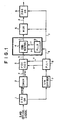
- Fig. 1 is a block diagram showing a coding apparatus configuration including an unused bit elimination device according to an embodiment of the present invention.
- a 2.4G (Fig. 1) optical signal is fed into 2.5G optical receiver (2.5G OR) 1 and is output from 2.6G optical sender (2.6G OS) 6 as a 2.6G optical signal through demultiplexer (DMUX) 2, FEC coder (FEC COD) 3, converter 4 and multiplexer (MUX) 5.
- DMUX demultiplexer
- FEC coder FEC COD
- MUX multiplexer
- the 2.4G optical signal is converted at the 2.5G optical receiver 1 into an STM16 signal in a form of an electric signal and is then fed to demultiplexer 2.
- Demultiplexer 2 separates the STM16 signal into STM1 signals a , of which there are 16 in number, and feeds them to FEC coder 3 in parallel.
- Fig. 2 shows the sixteen STM1 signals a , each of which consists of 238 bytes data.
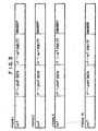
- Each STM1 signal a is encoded at FEC coder 3 into an FEC COD output signal b which includes overhead bit OH, parity bits which form a part of the FEC code, and unused bits, sometime termed dummy bits, as shown in Fig. 3.
- FEC COD output signal b is fed into multiplexer 5 and becomes a multiplexed signal in multiplexer 5.
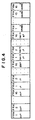
- Fig. 4 shows the multiplexed signal generated at multiplexer 5.
- the bit rate on the communication channel may be increased due to the unused bits.
- the FEC COD output signal b is fed into converter 4 for eliminating the unused bits.
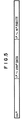
- Converter 4 outputs a signal c which does not include the additional unused bits, as shown in Fig. 5.
- Signal c consists of overhead bits, data and parities but does not include the unused bits as shown in the figure.
- Signal c is processed at multiplexer 5 into multiplexed signal d shown in Fig. 6.
- Multiplexed signal d is converted into the optical signal at 2.6G optical sender 6 and is sent out on the communication channel.
- a 155 MHz clock signal extracted at the 2.5G optical receiver 1 is fed to 1/N divider 7 and is divided into a long cycle signal of 81KHz.
- the 81 KHz signal is supplied to PLL 8 (PLL1).
- PLL 8 generates write clock e and read clock f of 166 MHz for use in the FEC coder 3 for FEC process.
- PLL 8 also sends a 2.6G multiplexing clock g to PLL 9 (PLL2).
- PLL 9 regenerates a 166 MHz clock from the 2.6G clock g and feeds write clock h and read clock i to converter 4 for eliminating the unused bits.
- the frequency of clock h is set to be lower than that of clock g .
- PLL 9 also supplies multiplexing clock i which synchronizes with clock i to multiplexer 5 and 2.6G optical sender 6.
- the multiplexed signal from which the unused bits are eliminated may be generated.
- Converter 4 and PLL 9 may be fabricated in one package IC.
- the IC may not be employed when a signal that includes the unused bits is transmitted.
- signal b is directly fed into multiplexer 5 and the 2.6G multiplexing clock g output from PLL 8 (PLL1) is directly fed to multiplexer 5 and the 2.6G optical sender 6.
- PLL 8 PLL1
- the configuration to transmit unused bits and another configuration not to transmit unused bits may be alternated with a switching means.
Landscapes
- Engineering & Computer Science (AREA)
- Computer Networks & Wireless Communication (AREA)
- Signal Processing (AREA)
- Time-Division Multiplex Systems (AREA)
- Dc Digital Transmission (AREA)
- Communication Control (AREA)
- Detection And Correction Of Errors (AREA)
- Detection And Prevention Of Errors In Transmission (AREA)
Claims (3)
- Kodierungsanordnung zum Erzeugen eines FEC-Kodeworts auf der Basis von Eingangsdaten, die eine Kodierungseinrichtung (3) zum fortlaufenden Ausgeben eines FEC-Kodeworts aufweist, das aus den Eingangsdaten und weiteren Paritäten und nicht verwendeten Bits besteht, welche nicht in dem FEC-Kodewort enthalten sind;
gekennzeichnet durch:eine Eliminierungsvorrichtung (4) für nicht verwendete Bits, um nur die nicht verwendeten Bits aus einer Kontinuität zu eliminieren, die aus dem FEC-Kodewort und den nicht verwendeten Dummy-Bits besteht, um nur das FEC-Kodewort auszugeben. - Kodierungsanordnung nach Anspruch 1, die ferner aufweist:wobei die Kodierungsanordnung (3) und die Eliminierungsvorrichtung (4) für nicht verwendete Bits für jede Ausgabe des Demultiplexers (2) arbeiten;eine Einrichtung (1) zum Umwandeln eines optischen Signals in elektrische Signaldaten;einen Demultiplexer (2) zum Demultiplexen der elektrischen Daten,
einen Multiplexer (5) zum Multiplexen von Ausgaben der Eliminierungsvorrichtung (4) für nicht verwendete Bits; und
eine Einrichtung (6) zum Umwandeln der Ausgabe des Multiplexers in ein optisches Signal. - Kodierungsanordnung nach Anspruch 1 oder 2, wobei die Kodierungsanordnung in ein Unterseekabelsystem eingebaut ist.
Applications Claiming Priority (2)
| Application Number | Priority Date | Filing Date | Title |
|---|---|---|---|
| JP9327398 | 1998-04-06 | ||
| JP09327398A JP3147078B2 (ja) | 1998-04-06 | 1998-04-06 | Fec符号語のダミービット除去装置及び符号化装置 |
Publications (3)
| Publication Number | Publication Date |
|---|---|
| EP0949778A2 EP0949778A2 (de) | 1999-10-13 |
| EP0949778A3 EP0949778A3 (de) | 2001-11-21 |
| EP0949778B1 true EP0949778B1 (de) | 2005-12-14 |
Family
ID=14077848
Family Applications (1)
| Application Number | Title | Priority Date | Filing Date |
|---|---|---|---|
| EP99302619A Expired - Lifetime EP0949778B1 (de) | 1998-04-06 | 1999-04-01 | Dummy-Bit-Eliminierungsvorrichtung und Kodierungsanordnung für FEC-Kodewort |
Country Status (3)
| Country | Link |
|---|---|
| US (1) | US6657967B1 (de) |
| EP (1) | EP0949778B1 (de) |
| JP (1) | JP3147078B2 (de) |
Families Citing this family (6)
| Publication number | Priority date | Publication date | Assignee | Title |
|---|---|---|---|---|
| US20020018444A1 (en) * | 2000-04-11 | 2002-02-14 | Cremin Con D. | Method and apparatus for multi-lane communication channel with deskewing capability |
| US6961350B1 (en) * | 2000-12-22 | 2005-11-01 | Applied Micro Circuits Corporation | System and method for segmenting a multidimensional digital frame structure |
| US6907560B2 (en) * | 2001-04-02 | 2005-06-14 | Nortel Networks Limited | Forward error correction (FEC) on a link between ICs |
| JP3863058B2 (ja) * | 2001-09-13 | 2006-12-27 | 三菱電機株式会社 | 光受信装置 |
| JP2003318865A (ja) * | 2002-04-26 | 2003-11-07 | Fuji Xerox Co Ltd | 信号伝送システム |
| US7644336B2 (en) | 2006-02-04 | 2010-01-05 | Hitachi Global Storage Technologies Netherlands, B.V. | Techniques for providing greater error protection to error-prone bits in codewords generated from irregular codes |
Family Cites Families (11)
| Publication number | Priority date | Publication date | Assignee | Title |
|---|---|---|---|---|
| US3700820A (en) * | 1966-04-15 | 1972-10-24 | Ibm | Adaptive digital communication system |
| US4755993A (en) * | 1986-07-16 | 1988-07-05 | Northern Telecom Limited | Transmission system using forward error correction |
| JPS63156447A (ja) | 1986-12-19 | 1988-06-29 | Fujitsu Ltd | フオワ−ドエラ−コレクシヨン回路 |
| JP2638091B2 (ja) * | 1988-06-24 | 1997-08-06 | ソニー株式会社 | データ伝送方法 |
| US5144304A (en) * | 1989-07-17 | 1992-09-01 | Digital Equipment Corporation | Data and forward error control coding techniques for digital signals |
| GB9024684D0 (en) * | 1990-11-13 | 1991-01-02 | Cognito Group Ltd | A method of communicating data |
| EP0684712B1 (de) * | 1994-05-17 | 2005-05-04 | Nippon Telegraph And Telephone Corporation | Endgerät in SDH Netzwerken unter Verwendung fehlerkorrigierender Codes |
| JP3645027B2 (ja) | 1995-09-20 | 2005-05-11 | 松下電器産業株式会社 | 可変長データ送受信装置 |
| US5862153A (en) * | 1995-09-29 | 1999-01-19 | Kabushiki Kaisha Toshiba | Coding apparatus and decoding apparatus for transmission/storage of information |
| JPH11298447A (ja) | 1998-04-08 | 1999-10-29 | Nec Corp | コーデックのフレームフォーマット、及びフレーム処理方法 |
| JP2000196567A (ja) | 1998-12-25 | 2000-07-14 | Matsushita Electric Ind Co Ltd | 送信装置、受信装置、伝送装置および伝送方法 |
-
1998
- 1998-04-06 JP JP09327398A patent/JP3147078B2/ja not_active Expired - Fee Related
-
1999
- 1999-04-01 EP EP99302619A patent/EP0949778B1/de not_active Expired - Lifetime
- 1999-04-05 US US09/285,775 patent/US6657967B1/en not_active Expired - Fee Related
Non-Patent Citations (1)
| Title |
|---|
| PETER SWEENEY: "MODIFICATIONS TO BLOCK CODES", ERROR CONTROL CODING: AN INTRODUCTION, 1991, PRENTICE HALL INTERNATIONAL, pages 36 - 39, XP000864253 * |
Also Published As
| Publication number | Publication date |
|---|---|
| JPH11296393A (ja) | 1999-10-29 |
| EP0949778A2 (de) | 1999-10-13 |
| JP3147078B2 (ja) | 2001-03-19 |
| EP0949778A3 (de) | 2001-11-21 |
| US6657967B1 (en) | 2003-12-02 |
Similar Documents
| Publication | Publication Date | Title |
|---|---|---|
| CA1232693A (en) | Network multiplex structure | |
| EP1117202B1 (de) | Verfahren zur Datenübertragung in Kommunikationssystemen | |
| EP0088432B1 (de) | Multiplexereinrichtung mit nBmB-Kodierer | |
| US7113703B2 (en) | Optical transmission system and optical transmission device | |
| US4750167A (en) | Digital audio transmission system | |
| US20030179783A1 (en) | Wavelength division multiplexing transmission system | |
| FI82348C (fi) | Kodare foer roerlig bild med fyllnadstecken med inre kodord. | |
| US6657967B1 (en) | Dummy bit elimination device and coding apparatus for FEC code word | |
| US4616361A (en) | Digital signal and multiplex device | |
| US7002957B2 (en) | Method of transporting frames of information between parts of a network through an intermediate network | |
| JP3597136B2 (ja) | 符号通信方法及び通信装置 | |
| JPS6333939A (ja) | 前方エラ−修正を使用する伝送システム | |
| EP0393514B1 (de) | Kanalzugriffssystem | |
| JPH0556025A (ja) | 伝送路符号処理方式 | |
| JPS63221729A (ja) | mBnB符号変換器を備えた多重変換装置 | |
| KR100237456B1 (ko) | 다중화를 위한 프레임 구조 | |
| JP4412479B2 (ja) | 信号多重方法及び装置 | |
| KR0171279B1 (ko) | 고속 데이터 전송장치의 오류 정정 방법 | |
| CA1048178A (en) | Digital multiplexing | |
| JP2001160792A (ja) | 時分割多重化データ通信システム | |
| GR3026720T3 (en) | Method and arrangement for generation of transmission multiplex signal and for synchronization of a reception multiplex signal on the transmission multiplex signal. | |
| JPH04258069A (ja) | ディジタル多重化装置 | |
| JPH02223238A (ja) | 音声信号伝送方式 | |
| JPH0321130A (ja) | 多重分離タイミング同期方式 | |
| JP2000209178A (ja) | 時分割多重回路及び時分割多重方法 |
Legal Events
| Date | Code | Title | Description |
|---|---|---|---|
| PUAI | Public reference made under article 153(3) epc to a published international application that has entered the european phase |
Free format text: ORIGINAL CODE: 0009012 |
|
| AK | Designated contracting states |
Kind code of ref document: A2 Designated state(s): AT BE CH CY DE DK ES FI FR GB GR IE IT LI LU MC NL PT SE Kind code of ref document: A2 Designated state(s): FR GB IT |
|
| AX | Request for extension of the european patent |
Free format text: AL;LT;LV;MK;RO;SI |
|
| PUAL | Search report despatched |
Free format text: ORIGINAL CODE: 0009013 |
|
| AK | Designated contracting states |
Kind code of ref document: A3 Designated state(s): AT BE CH CY DE DK ES FI FR GB GR IE IT LI LU MC NL PT SE |
|
| AX | Request for extension of the european patent |
Free format text: AL;LT;LV;MK;RO;SI |
|
| 17P | Request for examination filed |
Effective date: 20020121 |
|
| 17Q | First examination report despatched |
Effective date: 20020412 |
|
| AKX | Designation fees paid |
Free format text: FR GB IT |
|
| REG | Reference to a national code |
Ref country code: DE Ref legal event code: 8566 |
|
| GRAP | Despatch of communication of intention to grant a patent |
Free format text: ORIGINAL CODE: EPIDOSNIGR1 |
|
| RTI1 | Title (correction) |
Free format text: DUMMY BIT ELIMINATION DEVICE AND CODING APPARATUS FOR FEC CODE WORD |
|
| GRAS | Grant fee paid |
Free format text: ORIGINAL CODE: EPIDOSNIGR3 |
|
| GRAA | (expected) grant |
Free format text: ORIGINAL CODE: 0009210 |
|
| AK | Designated contracting states |
Kind code of ref document: B1 Designated state(s): FR GB IT |
|
| PG25 | Lapsed in a contracting state [announced via postgrant information from national office to epo] |
Ref country code: IT Free format text: LAPSE BECAUSE OF FAILURE TO SUBMIT A TRANSLATION OF THE DESCRIPTION OR TO PAY THE FEE WITHIN THE PRE;WARNING: LAPSES OF ITALIAN PATENTS WITH EFFECTIVE DATE BEFORE 2007 MAY HAVE OCCURRED AT ANY TIME BEFORE 2007. THE CORRECT EFFECTIVE DATE MAY BE DIFFERENT FROM THE ONE RECORDED.SCRIBED TIME-LIMIT Effective date: 20051214 |
|
| REG | Reference to a national code |
Ref country code: GB Ref legal event code: FG4D |
|
| ET | Fr: translation filed | ||
| PLBE | No opposition filed within time limit |
Free format text: ORIGINAL CODE: 0009261 |
|
| STAA | Information on the status of an ep patent application or granted ep patent |
Free format text: STATUS: NO OPPOSITION FILED WITHIN TIME LIMIT |
|
| 26N | No opposition filed |
Effective date: 20060915 |
|
| PGFP | Annual fee paid to national office [announced via postgrant information from national office to epo] |
Ref country code: GB Payment date: 20100325 Year of fee payment: 12 |
|
| PGFP | Annual fee paid to national office [announced via postgrant information from national office to epo] |
Ref country code: FR Payment date: 20100521 Year of fee payment: 12 |
|
| GBPC | Gb: european patent ceased through non-payment of renewal fee |
Effective date: 20110401 |
|
| REG | Reference to a national code |
Ref country code: FR Ref legal event code: ST Effective date: 20111230 |
|
| PG25 | Lapsed in a contracting state [announced via postgrant information from national office to epo] |
Ref country code: FR Free format text: LAPSE BECAUSE OF NON-PAYMENT OF DUE FEES Effective date: 20110502 |
|
| PG25 | Lapsed in a contracting state [announced via postgrant information from national office to epo] |
Ref country code: GB Free format text: LAPSE BECAUSE OF NON-PAYMENT OF DUE FEES Effective date: 20110401 |