EP0952603A2 - Farbkathodenstrahlröhre und deren Hertsellungsverfahren - Google Patents
Farbkathodenstrahlröhre und deren Hertsellungsverfahren Download PDFInfo
- Publication number
- EP0952603A2 EP0952603A2 EP99114180A EP99114180A EP0952603A2 EP 0952603 A2 EP0952603 A2 EP 0952603A2 EP 99114180 A EP99114180 A EP 99114180A EP 99114180 A EP99114180 A EP 99114180A EP 0952603 A2 EP0952603 A2 EP 0952603A2
- Authority
- EP
- European Patent Office
- Prior art keywords
- correction lens
- light
- ray tube
- display screen
- exposure
- Prior art date
- Legal status (The legal status is an assumption and is not a legal conclusion. Google has not performed a legal analysis and makes no representation as to the accuracy of the status listed.)
- Granted
Links
Images


Classifications
-
- H—ELECTRICITY
- H01—ELECTRIC ELEMENTS
- H01J—ELECTRIC DISCHARGE TUBES OR DISCHARGE LAMPS
- H01J9/00—Apparatus or processes specially adapted for the manufacture, installation, removal, maintenance of electric discharge tubes, discharge lamps, or parts thereof; Recovery of material from discharge tubes or lamps
- H01J9/20—Manufacture of screens on or from which an image or pattern is formed, picked up, converted or stored; Applying coatings to the vessel
- H01J9/22—Applying luminescent coatings
- H01J9/227—Applying luminescent coatings with luminescent material discontinuously arranged, e.g. in dots or lines
- H01J9/2271—Applying luminescent coatings with luminescent material discontinuously arranged, e.g. in dots or lines by photographic processes
- H01J9/2272—Devices for carrying out the processes, e.g. light houses
- H01J9/2273—Auxiliary lenses and filters
-
- H—ELECTRICITY
- H01—ELECTRIC ELEMENTS
- H01J—ELECTRIC DISCHARGE TUBES OR DISCHARGE LAMPS
- H01J29/00—Details of cathode-ray tubes or of electron-beam tubes of the types covered by group H01J31/00
- H01J29/02—Electrodes; Screens; Mounting, supporting, spacing or insulating thereof
- H01J29/10—Screens on or from which an image or pattern is formed, picked up, converted or stored
- H01J29/18—Luminescent screens
- H01J29/30—Luminescent screens with luminescent material discontinuously arranged, e.g. in dots, in lines
- H01J29/32—Luminescent screens with luminescent material discontinuously arranged, e.g. in dots, in lines with adjacent dots or lines of different luminescent material, e.g. for colour television
- H01J29/322—Luminescent screens with luminescent material discontinuously arranged, e.g. in dots, in lines with adjacent dots or lines of different luminescent material, e.g. for colour television with adjacent dots
Definitions
- the present invention relates to a color cathode-ray tube and a method for manufacturing the cathode-ray tube, and more particularly to a high quality of high-definition cathode-ray tube in which a correction lens for formation of a fluorescent dot pattern of the cathode-ray tube for use in a lithography or light exposure step of forming a fluorescent film of the color cathode-ray tube is improved to obtain a high quality of high-definition cathode-ray tube as well as also to a method for manufacturing the cathode-ray tube.
- a multiplicity of stripe- or dot-like holes are left to form a black body and a stripe- or dot-like fluorescent film is formed for the holes.
- the holes should coincide with the fluorescent film in their position, for which reason it becomes vital to accurately position the both with respect to the electronic beam irradiation position.
- correction must be carried out simultaneously both in the horizontal and vertical directions, for which end such various correction lenses as to provide optimum correction have been used.
- Fig. 8 Shown in Fig. 8 is a structure of a light exposure base 84 in which a light source 81, a lens 82 and a correction lens 83 are incorporated, and on which a face panel 85 having a shadow mask 87 is mounted.
- the correction lens 83 which has a plan shape and cross-sectional shapes tilted in horizontal (X) and vertical (Y) directions, is made up of a plurality of square or rectangular blocks divided in the respective direction, as shown in Fig. 9, (a) to (c).
- An exposure beam emitted from the light source 81 is passed through the lens 82, refracted by the correction lens 83, and then reaches the inner surface of the face panel 85 through an aperture of the shadow mask 87 for light exposure of a photosensitive film 86.
- the correction lens 83 is vibrated in the two X and Y directions during the light exposure.
- the influence of the latticed dark line pattern disables accurater dot formation.
- One of such suggested methods is a correction lens as disclosed in, e.g., JP-A- 62-154525, which lens configuration will be explained below.
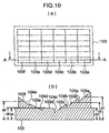
- Fig. 10 is a cross-sectional view of a correction lens which can suppress a latticed dark line pattern to some extent.
- the effective surface of the correction lens is divided into a plurality of regions in such a manner that a region 103a has a thickness d1 in its center, a region 103b has a thickness d2 in its center, a region 103c has a thickness d3 in its center, a region 103d has a thickness d4 in its center, a region 103e has a thickness d5 in its center, and a region 103f has a thickness d6 in its center.
- level differences 104a, 104b, 104c, 104d and 104e between the regions having the thicknesses d1, d2, d3, d4, d5 and d6 are set to be about 100 ⁇ m.
- the correction lens is designed so that the contrast and surface area of a latticed dark line pattern (striped dark line pattern) on the fluorescent screen are made small by making small the respective level differences.
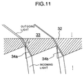
- Fig. 11 is a magnified cross-sectional view of a part of a conventional correction lens 33 (the central thicknesses of respective regions being shown as ignored).
- the conventional correction lens 33 has region boundaries 34a and 34b formed perpendicular to a reference plane 32. Therefore, as shown in Fig. 3, (a), light is emitted from a light source so that incident light obliquely directed into the region boundaries 34a and 34b of the correction lens 33 is subjected to secondary refraction. As a result, the light is locally converged or dispersed so that the quantity of exit light varies and thus dark lines having a width t depending on the height of the region boundaries are produced.
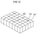
- Fig. 12 is a perspective view of a mold for use in molding the above correction lens based on a prior art technique.
- a mold 121 for the correction lens has a plurality of desired divided regions (such as 123) corresponding to those of the correction lens to be mold, the regions having respective region boundaries (such as 124).
- the mold based on the prior art technique is of a so-called assembled type which comprises a combination of several hundreds of blocks corresponding to the above regions. Therefore, it is highly difficult to make small the surface areas of the divided regions of the correction lens or to make smaller the level differences of the region boundaries in order to meet the higher definition requirement.
- the above object is attained by making a correction lens having a plurality of planar or curved faces differently tilted with respect to incident exposure light to cause the width and contrast of a latticed light/dark line pattern generated through the correction lens to become uniform all over the entire light exposure surface, the light exposure being carried out during vibration of the correction lens.
- the plurality of differently-tilted planar or curved faces formed on the correction lens of the invention are made more finely in dimensions when compared with those of the prior art correction lens, i.e., made to be half, 1/3 or less of the prior art dimensions. And the level differences of boundaries of the planar or curved faces are made as small as possible so that;
- the width and contrast of the latticed light/dark line or dark line pattern generated by the correction lens are made constant all over the light exposure surface, when light exposure irradiation is carried out during vibration of the correction lens, the quantity of light irradiated on the light exposure surface in a constant light exposure time becomes constant throughout the entire light exposure surface.
- the quantity of exposure light is made constant in this way, a good fluorescent film of dot pattern having good positional and configuration accuracies is formed on the face panel of the cathode-ray tube.
- the line width and contrast of latticed light and dark lines generated by the correction lens having the plurality of fine planar or curved faces formed thereon are made constant and uniform all over the light exposure surface on the shadow mask, when light exposure is carried out during vibration of the correction lens, a fluorescent dot pattern having good configuration and positional accuracies can be formed and thus a cathode-ray tube having a good quality of display screen can be obtained.
- cathode-ray tubes enables production of high-definition television sets and terminal monitors.
- Fig. 1 is a perspective view of an appearance of a correction lens in accordance with an embodiment of the present invention
- Fig. 2 is a cross-sectional view of the correction lens.
- a correction lens 3 which is made of such optical plastic having a high light transmissivity as polymethyl metaacrylate, is provided on its reference surface 2 with a collection of a plurality of planar or curved faces 3a having different tilts with respect to X and Y directions of the reference surface 2.
- the correction lens of the present invention shown in Fig. 1 has a configuration similar to that of such a conventional correction lens manufactured by a prior art technique as shown in Fig. 9, but different from the prior art correction lens in that the prior art correction lens is manufactured by making the planar or curved faces with use of a mold assembly of respectively separate molds, whereas, the correction lens of the present invention is manufactured by making the planar or curved faces with use of a single mold having these planar or curved faces machined in its inner surface.
- the present invention can avoid the restrictions imposed on the prior art when a plurality of planar or curved faces 3a having different tilts are made in the correction lens 3 with use of the assembled type mold of the submolds having the minimum dimensions corresponding to the respective sides of the planar or curved faces. That is, in the present invention, the side dimensions of the planar or curved faces 3a can be made finely to be half, 1/3 or less of those made with use of the prior art assembled type mold.
- planar or curved faces are positioned so that the value of biggest one of level differences at boundaries of the respective planar or curved faces having the different tilt angles becomes smallest, under which conditions the working conditions of the aforementioned integral correction lens are determined.
- the level differences at the boundaries which have been 100- or so in the prior art correction lens made with use of the assembled type mold, can be made to be 5 ⁇ m or less.
- level differences 4a at the boundaries of the lens faces can be made with a desired angle depending on the degree of generation of latticed light and dark lines by the level differences 4a.
- Fig. 3 shows magnified cross-sectional views of parts of a prior art correction lens and a correction lens of the present invention for comparison in light exposure effect therebetween.
- a level difference 34a at boundaries of lens faces of the prior art correction lens is formed to be vertical to a reference plane 32 and the incident angle of exposure light directed onto the level difference 34a varies with its incident place.
- the secondary refraction of the incident light obliquely directed onto the level difference 34a causes the light to be locally converged or dispersed, which undesirably results in that the light quantity and width of the resultant latticed light and dark lines of the incident light will vary with its place (or will be distributed).
- the level difference 4a is made smaller than that of the prior art correction lens, i.e., to be 1/20 or less thereof; the light quantity and width of the resultant latticed light and dark lines generated by the exposure light transmitted through the correction lens of the present invention can be made substantially constant throughout the entire exposure surface.
- Fig. 3, (b) is when the correction lens of the present invention is formed so that the tilt direction of the level difference 4a is parallel to the incident direction of the exposure light directed to the correction lens.
- the secondary-refraction percentage of the incident light at the level difference faces can be lessened.
- the quantity of light of the latticed light and dark lines generated by the secondary refraction can be reduced substantially constant all over the light exposure surface and the width of the light and dark lines can also be made narrow or substantially constant all over the light exposure surface.
- Fig. 13 Shown in Fig. 13 is a perspective view showing an appearance of a mold for use in molding the correction lens of Fig. 1 in accordance with an embodiment of the present invention.
- a mold 131 such non-ferrous soft metal as aluminum alloy, brass or copper is suitable from the viewpoint of its processability or machinability.
- the surface of the mold 131 is formed to correspond to the transfer surface of the correction lens shown in Fig. 1.
- Fig. 14 shows a machine for machining the mold for fabrication of the correction lens of the present invention
- Fig. 15 shows a flowchart for explaining the machining process of the mold of the present invention.
- the mold 131 is secured onto a pitch-direction positioning table or Z table 143.
- the transfer surface having the aforementioned surface configuration of the correction lens is cut in the surface of the mold with use of such a cutting tool as a diamond cutting tool 144.
- the diamond cutting tool 144 is held to a rotary table 142 so that the center of a cutting edge at a tip end of the cutting tool rotates on the center of the rotary table as a rotary center, whereby a motion of a table 141 toward the mold 131 in a Y direction provides a cutting thereto and a continuous motion of the table 141 in an X direction provides a cutting feed.
- the height of the level difference 4a of the discontinuous boundaries is previously calculated on the basis of the tilt angle of the planar or curved faces 3a of the correction lens 3 of the present invention and the optimum configuration or shape of the correction lens 3 is previously determined so that the value of highest one of level differences becomes smallest.
- the incident angle of light emitted from a light source is calculated to find a contact point tangent to the adjacent tilt face based on trigonometry, and the machining conditions are determined so that the value of maximum one of the level differences becomes smallest and the tilt direction of the side wall of corresponding one of the boundaries of the lens faces becomes parallel to the incident direction of the exposure light emitted from the light source.
- Such cycle is sequentially repeated until machining positions at the level differences at the discontinuous boundaries are all determined, after which the mold cutting is carried out.
- the pitch feed of the Z table 143 is carried out so that the position or attitude of the diamond cutting tool 144 is sequentially changed by the rotary table 142 during the cutting operation to the desired Y-direction tilt angle of the planar or curved face 133 to be next machined.
- the length of the cutting edge of the diamond cutting tool 144 perpendicular to the cutting direction X may correspond substantially to the length of one side of the desired planar or curved face 133 in the cutting width direction.
- Fig. 16 Shown in Fig. 16 is a machine for plastic working a mold for a correction lens of the present invention. More specifically, a mold 164 is held on a positioning table 163 mounted movably in two axial directions of X and Y tables perpendicular to each other. A punch 165 for making on the surface of the mold a plurality of planar or curved faces 133 having different tilt angles with respect to a reference bottom surface 132 is fixedly mounted to goniostages 166 and 167 rotably on the surface to be worked by the punch. The goniostages are mounted to a lower end of a Z shaft 168 movable in the vertical direction. Also mounted to the lower end of the Z shaft 168 is a controller 169 which includes a force sensor for controlling and managing a depressing force of the punch 165 toward the working surface. The Z shaft 168 is carried by a column 170.
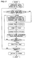
- Fig. 17 is a flowchart for explaining a process of plastic working a mold of the present invention.
- the height of a level difference 134 at the discontinuous boundaries is previously calculated on the basis of the tilt angle of the planar or curved face 133 to be machined to thereby determine such a machining position as to cause the level difference to be minimum.
- the incident angle of light emitted from a light source is calculated to find a contact point tangent to the adjacent tilt face based on trigonometry, and the machining conditions are determined so that the level differences becomes smallest and the tilt direction of the side wall of the boundary of the corresponding lens face becomes parallel to the incident direction of the exposure light emitted from the light source. This cycle is repeated until the machining positions of the level differences at all the discontinuous boundaries are determined, after which the mold machining is started.
- the material of the punch 165 material having a high hardness such as diamond, CBN or carbide material is suitably employed.
- the surface configuration of a lower end of the punch contributing to the mold machining is previously made to correspond to the desired transfer configuration of the planar or curved face 133.
- the goniostage 166 in the X direction and the goniostage 167 in the Y direction are positioned by respective drive sources such as pulse motors so that the attitude or orientation of the punch 165 to the mold 164 coincides with the X- and Y-directional tilts with respect to the reference bottom surface 132 requested by the surface to be machined. Relative positioning of the punch and the mold 164 in an X-Y plane is carried out by driving the X and Y tables.
- the Z shaft 168 holding the punch 165 thereon is lowered to depress the surface of the mold 164 to thereby form the desired planar or curved face 133 while the controller 169 including a force sensor controls and manages the depressing force, after which the attitude of the punch 165 is changed to form the level difference configuration of the lens face boundary.
- This cycle is sequentially repeated to machine the mold.
- the aforementioned machining is based on the plastic machining to form the mold for the correction lens of the present invention.
- the mold is supplied with optical plastic having a high light transmissivity such as polymethyl metaacrylate as mentioned earlier, or thermosetting resin, and then heated and compressed to mold a resultant correction lens.
- optical plastic having a high light transmissivity such as polymethyl metaacrylate as mentioned earlier, or thermosetting resin
- ultraviolet-ray setting resin may be supplied onto the surface of the mold and ultraviolet ray may be irradiated thereon to form the resultant correction lens.
- the above mold may be made not only by the aforementioned plastic working or cutting but also by electro-discharge machining.
- This method for forming the dot pattern of the phosphor-material dot pattern is the same as the method explained in conjunction with Fig. 8 in the above "Description of the Related Art", in which, in the present invention, a prior art correction lens 83 in Fig. 8 is replaced by the correction lens 3 of the present invention, exposure light (shown by a dotted line) emitted from a light source 81 is transmitted through a lens 82 and the correction lens 3 to be irradiated onto a shadow mask 87.
- the exposure light is uniformly irradiated onto the shadow mask 87 within a predetermined time, which results in that the exposure light passed through the shadow mask 87 is evenly irradiated on the photosensitive material film at the inner surface of the face panel of the cathode-ray tube all over the light exposure surface, with uniform distribution of the quantity of light irradiated.
- a phosphor dot pattern having a good positional accuracy and a configuration accuracy is formed on the inner surface of the face panel of the cathode-ray tube.
- Fig. 21 shows the light exposure effects of different correction lenses of the present invention and prior art for comparison therebetween when these correction lenses are used to form phosphor dot patterns on the inner surfaces of the face panels of respective resultant cathode-ray tubes.
- the above light exposure effect comparison was carried out by evenly illuminating light onto the inner surface 86 of the face panel 85 of the cathode-ray tube having the phosphor dot pattern formed thereon from its rear side under the respective conditions, by detecting the surface of the face panel with use of a television camera installed on the front side of the face panel to obtain an image signal, and then by processing the detected image signal on a pixel basis.
- the face panel 85 of the cathode-ray tube manufactured according to the above method generally tends to produce line-like luminosity irregularities in its vertical direction (corresponding to the Y direction in Fig. 21).
- a signal of pixels in the vertical direction was added to the image signal to evaluate luminosity fluctuation in the horizontal direction (corresponding to the X direction in Fig 21).
- Luminosity fluctuation d (luminosity)/dx
- Luminosity fluctuation factor (luminosity fluctuation/y-direction projection pixel number)/(average luminosity of cathode-ray tube measurement screen) x 100
- the luminosity fluctuation defined above has a good correlation with the luminous line irregularities confirmed when the predetermined range 211 of the cathode-ray tube fluorescent screen 210 to be measured is visually observed. It has been experimentally found by the inventors of the present application that, in order to obtain a high-quality cathode-ray tube, its luminosity fluctuation should be made small and its luminosity fluctuation factor should be made to be ⁇ 0.15% or less.
- the length of one side of the planar or curved faces of the surface of the correction lens for light exposure was made to be half or 1/3 or less of that of the prior art, the level difference at the boundaries of a plurality of different planar or curved faces having different tilts with respect to the reference plane was minimized so that the energy of light irradiated on the light exposure surface during the formation of the fluorescent screen pattern does not vary from place to place, the tilt direction of the side wall of each of the boundaries was set to be parallel to the optical path of incident light directed from the light source, light exposure was carried out during the vibration of the correction lens.
- the luminosity fluctuation factor was made to be ⁇ 0.05% or less when compared with ⁇ 0.35% in the prior art correction lens, and thus the intended target of obtaining a luminosity fluctuation factor of ⁇ 0.15% or less was attained.
- Fig. 21 Shown in Fig. 21 is a typical example of the present invention.
- a plurality of face panels of cathode-ray tubes were prepared based on the foregoing embodiment, their luminosity fluctuations were measured and then their luminosity fluctuation factors were found.
- the above target of obtaining a luminosity fluctuation factor of ⁇ 0.15% or less was realized.
- Fig. 4 is a perspective view of an appearance of a correction lens in accordance with another embodiment of the present invention.
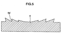
- Fig. 5 is a cross-sectional view of the correction lens of the embodiment of Fig. 4.
- Fig. 6 is a partially magnified cross-sectional view of a prior art correction lens.
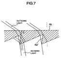
- Fig. 7 is a partially magnified cross-sectional view of the embodiment of Fig. 5.
- a correction lens 4 which is made of optical plastic having a high light transmissivity such as polymethyl metaacrylate, comprises a combination of a plurality of planar or curved faces 4b having different tilts in X and Y directions with respect to a reference plane 4c.
- the correction lens of Fig. 4 has a shape similar to that of the correction lens manufactured by the prior art technique, but is different from the prior art correction lens in that, as shown in Fig. 7, an angle ⁇ of a level difference face 4a'' at the boundaries of the plurality of differently-tilted planar or curved faces of the correction lens with respect to the reference plane 4c is constant with respect to exposure light incident at an angle of 120 degrees or less.
- an angle ⁇ of a level difference face 4a'' at the boundaries of the plurality of differently-tilted planar or curved faces of the correction lens with respect to the reference plane 4c is constant with respect to exposure light incident at an angle of 120 degrees or less.
- a mold is provided therein with a transfer surface having a configuration corresponding to the divided planar or curved faces of a correction lens
- the height of the level difference at boundaries of regions having a plurality of planar or curved faces having different tilt angles can be made to be 5 ⁇ m or less.
- a correction lens made of soft optical plastic material can be molded in the mold and then be released from the mold.
- the parts at which the exiting light is affected by the above region boundaries are formed therein with a predetermined width of lines, scratches or the like to make the face rough and to scatter the exposure light, whereby there can be complemented an irregularity in the width of the latticed dark line pattern which is major one of causes of generating variations during the molding of the dot pattern.
- the angle ⁇ may be made constant.
- the correction lens 4 it is sufficient to make uniform, all over the light exposure surface, the line width and contrast of the dark line pattern generated on the exposure light surface by the exposure light passed through the correction lens 4 and reaching the exposure light surface.
- Fig. 18 is a perspective view of a mold for use in molding the correction lens of Fig. 4 according to the embodiment of the present invention, showing its appearance.
- non-ferrous soft metal such as, e.g., aluminum alloy, brass or copper is suitably employed from the viewpoint of its processability or machinability to be later explained.
- the lowermost point of a plurality of planar or curved faces 181a differently tilted relative to a reference bottom plane 181c is transferred as the uppermost point of the tilt surface of the resultant correction lens to be molded.
- the surface of the mold 181 is formed to correspond to the transfer surface of the correction lens shown in Fig. 1.
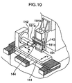
- Fig. 19 shows a machine for cutting into the mold for molding of the correction lens of the present invention.
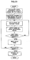
- Fig. 20 shows a flowchart for explaining the cutting process of the mold of the present invention.
- a mold 191 is fixedly mounted onto the Z table 143 for positioning of its pitch direction.
- One surface of the mold is cut with use of such a cutting tool as diamond tool or bit into the aforementioned transfer surface of the correction lens.
- the diamond cutting tool 144 is fixedly mounted to the rotary table 142 to be rotated around the center of the cutting edge of the tool at its tip end as a rotary center, so that a movement of the table 141 in the X direction with respect to the mold 181 causes a cutting while a continuous movement of the table 141 in the X direction causes a cutting feed.
- the angle ⁇ with respect to the reference plane is previously calculated on the basis of the uppermost point of the region boundary of the planar or curved faces to be processed, the number of lines and an optimum machining position are determined on the basis of the height of the planar or curved face 181a, this cycle is sequentially repeated to determine the machining positions for the level steps of all the discontinuous boundaries, after which the mold cutting is now started actually.
- pitch feed of the Z table 143 is effected so that the attitude of the diamond cutting tool 144 is sequentially changed by the rotary table 142 during the cutting to a desired Y-directional tilt angle of a planar or curved face 181b to be next cut.
- the length of the cutting edge of the diamond cutting tool 144 in a direction perpendicular to the cutting direction X is previously set to be equal to or somewhat longer than one side of the desired planar or curved face 181b.
- the mold made according to the above cutting system is supplied with optical plastic such as polymethyl metaacrylate or thermosetting resin having a high light transmissivity to one surface of the mold, and then is subjected to a heating and compressing process to thereby form a correction lens.
- optical plastic such as polymethyl metaacrylate or thermosetting resin having a high light transmissivity
- thermosetting resin having a high light transmissivity
- ultraviolet-ray setting resin may supplied to the surface of the mold and be subjected to an ultraviolet-ray irradiation to thereby form a correction lens.
- the method of forming the fluorescent dot pattern is the same as the method explained in the above 'Description of the Related Art' in connection with Fig. 8 as already explained even in the first embodiment. That is, in the present invention, the prior art correction lens 83 of Fig. 8 is replaced with the correction lens 4 of the present invention so that the exposure light (shown by the dotted line in the drawing) emitted from the light source 81 is passed through the lens 82 and correction lens 4 and then irradiated on the shadow mask 87.
- the tilt angle of the level difference or boundary face 4a'' or 4a' of the region boundary with respect to the reference plane 4c is made to be a constant obtuse angle, the surface roughness of the boundary face is deteriorated, or a constant width of lines or scratches are applied to the rear side of the region boundary to make the surface rough and to decrease the quantity of exposure light passed through the region boundary, whereby the width and contrast of a latticed line produced by the exposure light passed through the correction lens can be made desirably constant.
- the irradiation of the exposure light during the vibration of the correction lens 4 causes the exposure light to be uniformly irradiated on the shadow mask 87 in a predetermined time, whereby the exposure light passed through the shadow mask 87 can be irradiated on the photosensitive film on the inner surface of the face panel of the cathode-ray tube all over the light exposure surface with a uniform distribution of the quantity of light energy irradiated.
- a fluorescent dot pattern having good positional and configuration accuracies can be formed on the inner surface of the face panel of the cathode-ray tube.
- the color cathode-ray tube manufactured according to the present embodiment was subjected to light exposure effect measurements, which measurement results were substantially the same as those in the foregoing first embodiment.
- the present invention is not limited to the specific embodiments. That is, the correction lens for light exposure for formation of the fluorescent dot pattern at the inner surface of the face panel of the color cathode-ray tube according to the present invention is formed with the plurality of fine planar or curved faces so that the method disclosed in the first embodiment may be combined with the method disclosed in the second embodiment or part of these methods may be used, so long as the line width of a latticed light/dark line pattern or a dark line pattern generated on the light exposure surface when the exposure light is irradiated thereon as well as the contrast of the exposure light irradiated on these patterns and the light exposure surface other than the patterns become constant all over the light exposure surface.
- the line width of the light/dark pattern or dark line pattern as well as the contrast of the exposure light irradiated on these patterns and the light exposure surface other than the patterns are made constant and uniform over the entire light exposure surface.
- the line width of the latticed light and dark lines generated by the correction lens having the plurality of fine planar or curved faces thereon as well as the contrast thereof can be made uniform all over the light exposure surface on the shadow mask, the light exposure during the vibration of the correction lens enables the formation of a fluorescent dot pattern having good configuration and positional accuracies, which leads to a cathode-ray tube having a good quality of display.
- cathode-ray tubes enables production of high-definition television sets and terminal monitors.
Landscapes
- Engineering & Computer Science (AREA)
- Manufacturing & Machinery (AREA)
- Formation Of Various Coating Films On Cathode Ray Tubes And Lamps (AREA)
Applications Claiming Priority (5)
| Application Number | Priority Date | Filing Date | Title |
|---|---|---|---|
| JP510294 | 1994-01-21 | ||
| JP510294 | 1994-01-21 | ||
| JP20514894 | 1994-08-30 | ||
| JP20514894 | 1994-08-30 | ||
| EP95906497A EP0737996B1 (de) | 1994-01-21 | 1995-01-20 | Verfahren zur herstellung einer kathodenstrahlenröhre |
Related Parent Applications (2)
| Application Number | Title | Priority Date | Filing Date |
|---|---|---|---|
| EP95906497A Division EP0737996B1 (de) | 1994-01-21 | 1995-01-20 | Verfahren zur herstellung einer kathodenstrahlenröhre |
| EP95906497.3 Division | 1995-07-27 |
Publications (3)
| Publication Number | Publication Date |
|---|---|
| EP0952603A2 true EP0952603A2 (de) | 1999-10-27 |
| EP0952603A3 EP0952603A3 (de) | 2000-10-25 |
| EP0952603B1 EP0952603B1 (de) | 2006-11-22 |
Family
ID=26338996
Family Applications (2)
| Application Number | Title | Priority Date | Filing Date |
|---|---|---|---|
| EP95906497A Expired - Lifetime EP0737996B1 (de) | 1994-01-21 | 1995-01-20 | Verfahren zur herstellung einer kathodenstrahlenröhre |
| EP99114180A Expired - Lifetime EP0952603B1 (de) | 1994-01-21 | 1995-01-20 | Anzeigeschirm für eine Farbkathodenstrahlröhre |
Family Applications Before (1)
| Application Number | Title | Priority Date | Filing Date |
|---|---|---|---|
| EP95906497A Expired - Lifetime EP0737996B1 (de) | 1994-01-21 | 1995-01-20 | Verfahren zur herstellung einer kathodenstrahlenröhre |
Country Status (6)
| Country | Link |
|---|---|
| US (1) | US5844355A (de) |
| EP (2) | EP0737996B1 (de) |
| KR (1) | KR100231392B1 (de) |
| CN (2) | CN1153242C (de) |
| DE (2) | DE69535306T2 (de) |
| WO (1) | WO1995020239A1 (de) |
Families Citing this family (5)
| Publication number | Priority date | Publication date | Assignee | Title |
|---|---|---|---|---|
| DE69529334T2 (de) | 1994-09-09 | 2003-10-16 | Koninklijke Philips Electronics N.V., Eindhoven | Verfahren zum herstellen einer form zur verwendung in der herstellung eines optischen elements, das optische unterelemente in musterform angeordnet enthält und vorrichtung zur durchführung des verfahrens |
| JPH09320466A (ja) * | 1996-05-29 | 1997-12-12 | Hitachi Ltd | 高精細カラ−ブラウン管とその製造方法 |
| TW460900B (en) * | 1999-04-16 | 2001-10-21 | Koninkl Philips Electronics Nv | Method of producing a screen for a display device, screen for a display device produced by means of said method and display device provided with said screen |
| TW561307B (en) * | 2000-06-26 | 2003-11-11 | Koninkl Philips Electronics Nv | A method of producing a segmented lens, a segmented lens, a mould, a method of producing a screen, a screen of a colour display tube and a colour display tube provided with a screen |
| US7312928B2 (en) * | 2005-10-01 | 2007-12-25 | Hewlett-Packard Development Company, L.P. | Projection system field lens |
Family Cites Families (8)
| Publication number | Priority date | Publication date | Assignee | Title |
|---|---|---|---|---|
| US3592112A (en) * | 1969-07-25 | 1971-07-13 | Rca Corp | Photographic printing of cathode-ray tube screen structure |
| US4052123A (en) * | 1971-11-29 | 1977-10-04 | Hitachi, Ltd. | Correcting lenses utilized in the manufacture of fluorescent screen of color picture tubes |
| JPS4998174A (de) * | 1973-01-19 | 1974-09-17 | ||
| JPS5357966A (en) * | 1976-11-05 | 1978-05-25 | Hitachi Ltd | Manufacture for color receiving tube |
| JPS62154525A (ja) * | 1985-12-27 | 1987-07-09 | Toshiba Corp | 補正レンズ |
| GB8712458D0 (en) * | 1987-05-27 | 1987-07-01 | Philips Nv | Producing colour picture tube screen |
| JPH0388233A (ja) * | 1989-08-30 | 1991-04-12 | Toshiba Corp | カラー受像管の蛍光面形成用補正レンズの製作方法 |
| JPH04284328A (ja) * | 1991-03-13 | 1992-10-08 | Hitachi Ltd | カラー陰極線管螢光面露光用補正レンズ |
-
1995
- 1995-01-20 EP EP95906497A patent/EP0737996B1/de not_active Expired - Lifetime
- 1995-01-20 WO PCT/JP1995/000058 patent/WO1995020239A1/ja not_active Ceased
- 1995-01-20 DE DE69535306T patent/DE69535306T2/de not_active Expired - Fee Related
- 1995-01-20 KR KR1019960703899A patent/KR100231392B1/ko not_active Expired - Fee Related
- 1995-01-20 DE DE69520875T patent/DE69520875T2/de not_active Expired - Fee Related
- 1995-01-20 US US08/676,341 patent/US5844355A/en not_active Expired - Fee Related
- 1995-01-20 EP EP99114180A patent/EP0952603B1/de not_active Expired - Lifetime
- 1995-01-20 CN CNB951920669A patent/CN1153242C/zh not_active Expired - Fee Related
- 1995-01-20 CN CNB03122329XA patent/CN1267957C/zh not_active Expired - Fee Related
Also Published As
| Publication number | Publication date |
|---|---|
| KR970700927A (ko) | 1997-02-12 |
| CN1267957C (zh) | 2006-08-02 |
| US5844355A (en) | 1998-12-01 |
| CN1153242C (zh) | 2004-06-09 |
| WO1995020239A1 (en) | 1995-07-27 |
| DE69535306T2 (de) | 2007-06-21 |
| EP0952603B1 (de) | 2006-11-22 |
| DE69535306D1 (de) | 2007-01-04 |
| DE69520875D1 (de) | 2001-06-13 |
| KR100231392B1 (ko) | 1999-11-15 |
| EP0952603A3 (de) | 2000-10-25 |
| EP0737996A1 (de) | 1996-10-16 |
| CN1501431A (zh) | 2004-06-02 |
| CN1144014A (zh) | 1997-02-26 |
| DE69520875T2 (de) | 2001-09-13 |
| EP0737996A4 (de) | 1997-04-16 |
| EP0737996B1 (de) | 2001-05-09 |
Similar Documents
| Publication | Publication Date | Title |
|---|---|---|
| KR100378767B1 (ko) | 투과형 스크린 | |
| EP0734314B1 (de) | Verfahren zum herstellen einer form zur verwendung in der herstellung eines optischen elements, das optische unterelemente in musterform angeordnet enthält und vorrichtung zur durchführung des verfahrens | |
| EP0952603B1 (de) | Anzeigeschirm für eine Farbkathodenstrahlröhre | |
| KR100236877B1 (ko) | 컬러브라운 관 및 컬러디스플레이장치 | |
| JP3123381B2 (ja) | カラーブラウン管の製造方法及びカラーディスプレイ装置の製造方法 | |
| JP3422322B2 (ja) | カラーブラウン管及びカラーディスプレイ装置 | |
| JP3233133B2 (ja) | カラーブラウン管及びカラーディスプレイ装置 | |
| KR100288034B1 (ko) | 고선명도음극선관및그의제조방법 | |
| GB1598084A (en) | Exposure device for making a stripe screen on a faceplate of a colour cathode ray tube | |
| EP0415286B1 (de) | Korrektionslinsenherstellungsverfahren zur Erzeugung einer Phosphorschicht auf der Stirnseite einer Kathodenstrahlfarbröhre | |
| EP0654813A1 (de) | Gerät zur Musteraufzeichnung mittels Elektronenstrahl und Mustersaufzeichnungsverfahren unter Verwendung eines solchen Geräts | |
| JPH06267414A (ja) | ブラウン管螢光面パターン形成用補正レンズ及びその金型 | |
| EP0400629A1 (de) | Verfahren zur Herstellung einer Farbkathodenstrahlröhre und Belichtungseinrichtung zur Verwendung bei Einsatz dieses Verfahrens | |
| JP2003217471A (ja) | カラーブラウン管及びカラーディスプレイ装置 | |
| JPH06314541A (ja) | ブラウン管蛍光面パターン形成用補正レンズとその金型の製作方法及び同補正レンズの成形方法 | |
| JPH05217498A (ja) | 螢光面パターン形成用補正レンズとその成形方法、およびその金型と金型の加工方法並びに加工装置 | |
| JP3905877B2 (ja) | リアプロジェクションディスプレイ用スクリーンに用いるマイクロレンズアレイ用母型の製造方法 | |
| KR100188346B1 (ko) | 보정렌즈 제작용 몰드와 이것에 의해서 제작된 보정렌즈 및 그 제조방법 | |
| JP2763571B2 (ja) | カラー受像管蛍光面形成用補正レンズ | |
| JPH0765720A (ja) | カラーブラウン管螢光面パターン形成用補正レンズ | |
| JP2000258843A (ja) | レンズシート用成形型の製造方法及びレンズシート用成形型 | |
| JPH04284328A (ja) | カラー陰極線管螢光面露光用補正レンズ | |
| JPH0218836A (ja) | カラー陰極線管の蛍光面作成装置 | |
| JPH07288082A (ja) | 陰極線管のパネル蛍光面作製用補正レンズ | |
| JPH04123747A (ja) | カラー受像管の製造方法 |
Legal Events
| Date | Code | Title | Description |
|---|---|---|---|
| PUAI | Public reference made under article 153(3) epc to a published international application that has entered the european phase |
Free format text: ORIGINAL CODE: 0009012 |
|
| 17P | Request for examination filed |
Effective date: 19990722 |
|
| AC | Divisional application: reference to earlier application |
Ref document number: 737996 Country of ref document: EP |
|
| AK | Designated contracting states |
Kind code of ref document: A2 Designated state(s): DE FR GB |
|
| RIN1 | Information on inventor provided before grant (corrected) |
Inventor name: NISHIGUCHI, TAKASHI Inventor name: WANG, YING-FU, HACHIMANYAMA-APART 433 |
|
| PUAL | Search report despatched |
Free format text: ORIGINAL CODE: 0009013 |
|
| AK | Designated contracting states |
Kind code of ref document: A3 Designated state(s): AT BE CH DE DK ES FR GB GR IE IT LI LU MC NL PT SE |
|
| RIC1 | Information provided on ipc code assigned before grant |
Free format text: 7H 01J 9/227 A, 7H 01J 29/18 B, 7H 01J 29/32 B |
|
| AKX | Designation fees paid |
Free format text: DE FR GB |
|
| RTI1 | Title (correction) |
Free format text: DISPLAY SCREEN FOR A COLOUR CATHODE-RAY TUBE |
|
| 17Q | First examination report despatched |
Effective date: 20031021 |
|
| GRAP | Despatch of communication of intention to grant a patent |
Free format text: ORIGINAL CODE: EPIDOSNIGR1 |
|
| GRAS | Grant fee paid |
Free format text: ORIGINAL CODE: EPIDOSNIGR3 |
|
| GRAA | (expected) grant |
Free format text: ORIGINAL CODE: 0009210 |
|
| AC | Divisional application: reference to earlier application |
Ref document number: 0737996 Country of ref document: EP Kind code of ref document: P |
|
| AK | Designated contracting states |
Kind code of ref document: B1 Designated state(s): DE FR GB |
|
| REG | Reference to a national code |
Ref country code: GB Ref legal event code: FG4D |
|
| PGFP | Annual fee paid to national office [announced via postgrant information from national office to epo] |
Ref country code: GB Payment date: 20061220 Year of fee payment: 13 Ref country code: FR Payment date: 20061220 Year of fee payment: 13 |
|
| REF | Corresponds to: |
Ref document number: 69535306 Country of ref document: DE Date of ref document: 20070104 Kind code of ref document: P |
|
| PGFP | Annual fee paid to national office [announced via postgrant information from national office to epo] |
Ref country code: DE Payment date: 20070201 Year of fee payment: 13 |
|
| ET | Fr: translation filed | ||
| PLBE | No opposition filed within time limit |
Free format text: ORIGINAL CODE: 0009261 |
|
| STAA | Information on the status of an ep patent application or granted ep patent |
Free format text: STATUS: NO OPPOSITION FILED WITHIN TIME LIMIT |
|
| 26N | No opposition filed |
Effective date: 20070823 |
|
| GBPC | Gb: european patent ceased through non-payment of renewal fee |
Effective date: 20080120 |
|
| PG25 | Lapsed in a contracting state [announced via postgrant information from national office to epo] |
Ref country code: DE Free format text: LAPSE BECAUSE OF NON-PAYMENT OF DUE FEES Effective date: 20080801 |
|
| REG | Reference to a national code |
Ref country code: FR Ref legal event code: ST Effective date: 20081029 |
|
| PG25 | Lapsed in a contracting state [announced via postgrant information from national office to epo] |
Ref country code: GB Free format text: LAPSE BECAUSE OF NON-PAYMENT OF DUE FEES Effective date: 20080120 |
|
| PG25 | Lapsed in a contracting state [announced via postgrant information from national office to epo] |
Ref country code: FR Free format text: LAPSE BECAUSE OF NON-PAYMENT OF DUE FEES Effective date: 20080131 |