EP0953985A2 - Nichtflüchtige Halbleiterspeicheranordnung - Google Patents
Nichtflüchtige Halbleiterspeicheranordnung Download PDFInfo
- Publication number
- EP0953985A2 EP0953985A2 EP99108242A EP99108242A EP0953985A2 EP 0953985 A2 EP0953985 A2 EP 0953985A2 EP 99108242 A EP99108242 A EP 99108242A EP 99108242 A EP99108242 A EP 99108242A EP 0953985 A2 EP0953985 A2 EP 0953985A2
- Authority
- EP
- European Patent Office
- Prior art keywords
- memory cell
- voltage
- reference cell
- storage device
- semiconductor storage
- Prior art date
- Legal status (The legal status is an assumption and is not a legal conclusion. Google has not performed a legal analysis and makes no representation as to the accuracy of the status listed.)
- Withdrawn
Links
Images



Classifications
-
- H—ELECTRICITY
- H10—SEMICONDUCTOR DEVICES; ELECTRIC SOLID-STATE DEVICES NOT OTHERWISE PROVIDED FOR
- H10B—ELECTRONIC MEMORY DEVICES
- H10B69/00—Erasable-and-programmable ROM [EPROM] devices not provided for in groups H10B41/00 - H10B63/00, e.g. ultraviolet erasable-and-programmable ROM [UVEPROM] devices
-
- G—PHYSICS
- G11—INFORMATION STORAGE
- G11C—STATIC STORES
- G11C16/00—Erasable programmable read-only memories
- G11C16/02—Erasable programmable read-only memories electrically programmable
- G11C16/06—Auxiliary circuits, e.g. for writing into memory
- G11C16/34—Determination of programming status, e.g. threshold voltage, overprogramming or underprogramming, retention
- G11C16/3404—Convergence or correction of memory cell threshold voltages; Repair or recovery of overerased or overprogrammed cells
- G11C16/3409—Circuits or methods to recover overerased nonvolatile memory cells detected during erase verification, usually by means of a "soft" programming step
-
- G—PHYSICS
- G11—INFORMATION STORAGE
- G11C—STATIC STORES
- G11C16/00—Erasable programmable read-only memories
- G11C16/02—Erasable programmable read-only memories electrically programmable
- G11C16/06—Auxiliary circuits, e.g. for writing into memory
- G11C16/26—Sensing or reading circuits; Data output circuits
- G11C16/28—Sensing or reading circuits; Data output circuits using differential sensing or reference cells, e.g. dummy cells
-
- G—PHYSICS
- G11—INFORMATION STORAGE
- G11C—STATIC STORES
- G11C16/00—Erasable programmable read-only memories
- G11C16/02—Erasable programmable read-only memories electrically programmable
- G11C16/06—Auxiliary circuits, e.g. for writing into memory
- G11C16/34—Determination of programming status, e.g. threshold voltage, overprogramming or underprogramming, retention
- G11C16/3404—Convergence or correction of memory cell threshold voltages; Repair or recovery of overerased or overprogrammed cells
-
- G—PHYSICS
- G11—INFORMATION STORAGE
- G11C—STATIC STORES
- G11C16/00—Erasable programmable read-only memories
- G11C16/02—Erasable programmable read-only memories electrically programmable
- G11C16/06—Auxiliary circuits, e.g. for writing into memory
- G11C16/34—Determination of programming status, e.g. threshold voltage, overprogramming or underprogramming, retention
- G11C16/3436—Arrangements for verifying correct programming or erasure
-
- G—PHYSICS
- G11—INFORMATION STORAGE
- G11C—STATIC STORES
- G11C16/00—Erasable programmable read-only memories
- G11C16/02—Erasable programmable read-only memories electrically programmable
- G11C16/06—Auxiliary circuits, e.g. for writing into memory
- G11C16/34—Determination of programming status, e.g. threshold voltage, overprogramming or underprogramming, retention
- G11C16/3436—Arrangements for verifying correct programming or erasure
- G11C16/344—Arrangements for verifying correct erasure or for detecting overerased cells
- G11C16/3445—Circuits or methods to verify correct erasure of nonvolatile memory cells
-
- G—PHYSICS
- G11—INFORMATION STORAGE
- G11C—STATIC STORES
- G11C16/00—Erasable programmable read-only memories
- G11C16/02—Erasable programmable read-only memories electrically programmable
- G11C16/06—Auxiliary circuits, e.g. for writing into memory
- G11C16/34—Determination of programming status, e.g. threshold voltage, overprogramming or underprogramming, retention
- G11C16/3436—Arrangements for verifying correct programming or erasure
- G11C16/3454—Arrangements for verifying correct programming or for detecting overprogrammed cells
- G11C16/3459—Circuits or methods to verify correct programming of nonvolatile memory cells
Definitions
- This invention relates to a non-volatile semiconductor storage device and, more particularly, to an electrically erasable and programmable non-volatile semiconductor storage device, such as a flash EEPROM.
- UVPROM ultraviolet rays
- EEPROM electrically erasable and programmable ROM
- EEPROM electrically erasable and programmable ROM
- EEPROM electrically erasable and programmable ROM
- EEPROM electrically erasable and programmable ROM
- EEPROM electrically erasable and programmable ROM
- its reliability to programming and erasing is generally lower than ROM. Namely, program verify to ensure easily that no output exists after programming by charging electric charge into floating gate, and erase verify to ensure securely that certain output exists after erasing by discharging electric charge from floating gate become important matters.
- FIG.1 A conventional example of this kind of non-volatile semiconductor storage device is shown in FIG.1.
- This non-volatile semiconductor storage device is EEPROM disclosed in Japanese patent application laid-open No.5-36288 (1993).
- the reading output of a memory cell transistor TC00 etc. is led through a Y-gate transistor section B2 to a load transistor section B4, and the reading output of a dummy transistor TRD0 etc. is led through connection part B3 to a dummy load transistor section B5.
- the load transistor section B4, the dummy load transistor section B5 and a differential amplifier B6 compose a sense amplifier.
- the differential amplifier B6 outputs amplifying the difference between input IN1 from the load transistor section B4 and IN2 from the dummy load transistor section B5 when power-down signal line PD becomes "L" in its operation.
- the equivalent resistance value of the dummy load transistors TL1 and TL2 is a half of the equivalent resistance value of a load transistor TL0 on the load transistor section B4 side.
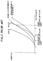
- the threshold voltage of the reference transistor TR is not built in accurately in the fabrication process, and in the program verify, the voltage of the reference transistor gate line XR is determined by many elements like the transistors TR0, TG1 etc. Also, since even in the verifying, the dummy load transistors TL1 and TL2 remain connected in parallel, its resistance is a half of the load transistor TL0. Further, in the verifying, the value of reference current is also small. Therefore, as shown in FIG.2 transcribed from FIG.2 of Japanese patent application laid-open No.5-36288 (1993), it operates in a region where the slope of current versus voltage curve for reference transistor TR is gentle, and has a large dispersion of operating point. Because of this, there is a problem that the judging condition in the program verifying is rougher than that in the reading and lacks in fineness.
- This problem may be not material to a general EEPROM whose erasing is conducted with the support of ultraviolet rays.
- flash EEPROM that has been used rapidly in the portable-use field with the recent popularization of personal computer and portable telephone, it is serious. Namely, the erasing of flash EEPROM is conducted by only an electrical means without the support of ultraviolet rays, and therefore a device structure suitable for that needs to be employed. So, the dispersion of erasing increases and there occurs an unevenness in erasing, which is not seen in the ultraviolet-ray erasing. Therefore, it is necessary to conduct the program verify finely. Also, adding to the erase verify, the over-erase verify also needs to be conducted.
- an electrically erasable and programmable non-volatile semiconductor storage device that data is read out comparing the output of a memory cell and the output of a reference cell by a sense amplifier, wherein:
- the threshold voltage of reference cell is built in so as to have an accurate value in the manufacturing process of the reference cell. This value is set to be the upper-limit value of threshold voltage for the erasing of memory cell in the same chip.
- the reference cell is made only one, and its gate voltage can be set independently of the gate voltage of memory cell.
- the sensitivity of sense amplifier is made symmetrical in the verifying. Therefore, with the simple device composition, the verifying can be conducted finely, which helps enhance the reliability of especially a flash EEPROM.
- a non-volatile semiconductor storage device is characterized that the reference cell is built in so that it has a given threshold voltage value, and the gate voltage of the memory cell and the gate voltage of the reference cell are allowed to be set independently.
- This dispersion occurs is mainly that the amount of electron to be injected into or extracted from the floating gate is dispersed due to a dispersion in voltage to be applied to the control gate or in application time, or a dispersion in film thickness or gate size of gate oxide film.
- the program verify to verify that the threshold voltage of memory cell in programming is higher than the lower-limit value (program verify level) and the erase verify to verify that the threshold voltage of memory cell after erasing is lower than the higher-limit value (erase verify level).
- program verify level the program verify and erase verify need to be conducted more accurately than that to a general EEPROM, as described earlier.
- the over-erase verify is also necessary.
- the over-erase means an excessive erasing, which causes that due to the excessive discharging of electric charge from the floating gate, the drain current flows even when the memory cell is of depletion type, i.e., even when the gate voltage is 0V, thereby the memory cell is sensed as if it is selected even when it is not selected actually. Therefore, the over-erase verify needs to verify that the threshold voltage of memory cell after erasing is higher than the lower-limit value (over-erase verify level).
- FIG.5 is a flow chart of the program verify and FIG.6 is a flow chart of the erase verify and over-erase verify.
- FIG.6 before erasing, all memory cells need to be programmed temporarily. This is because the amount of electron injected into the floating gate is different between a memory cell that stores "0" and a memory cell that stores "1", and therefore one cell comes into over-erasing when these cells are erased at once. After that, conducting the erasing, then the verifying is conducted. When the over-erasing is detected in the over-erase verify, the re-programming is conducted by charging a little electric charge into the floating gate to restore it.
- the gate voltage of memory cell when the gate voltage of memory cell is referenced, the relative difference between the gate voltage of memory cell and the gate voltage of reference cell increases in the order of program verify, erase verify and over-erase verify.
- the gate voltage of reference cell when the gate voltage of reference cell is referenced, it does in the inverse order.
- the sense amplifier is configured to be symmetrical in the verifying, where it is not performed that the dummy load transistors TL1 and TL2 operate simultaneously as shown in FIG.1. Therefore, it does not occur that the slope of the current versus gate voltage curve for reference cell transistor is gentler than that for memory cell transistor as shown in FIG.2.
- FIG.7 shows current versus gate voltage curves (dotted lines) for memory cell transistor and a current versus gate voltage curve (full line on the right) for reference cell transistor in the erase verify, and a current versus gate voltage curve (full line on the left) for reference cell transistor in the program verify. In FIG.7, all the slopes are same, therefore it will be understood that the sensitivity of sense amplifier is also same at both the memory cell side and the reference cell side.
- the gate voltage of memory cell is allowed to be equal to that of reference cell. This is because, since the threshold voltage is built in accurately to the erase verify level, output is securely obtained from ON memory cell having the normal distribution as shown in FIG.4 and because the sensitivity of sense amplifier is equal.
- FIG.8 is a block diagram showing a non-volatile semiconductor storage device in the preferred embodiment according to the invention.
- This device is composed of a memory cell array 101 that is a group of flash memory cells, a row decoder 102 to select a specific memory cell from the memory cell array 101, a column decoder 103, a column selector 104, a reference cell array 105 including one reference cell, a sense amplifier 107 to compare output of memory cell and output of reference cell, a timing circuit 108 to control the sense amplifier 107, a comparator 109 that conducts the verify judgement to the output DOUT of the sense amplifier 107 and outputs the verify judgement result, a verify voltage switching circuit 111 that switches the verify voltage according to an operation mode signal and supplies it to the row decoder 102 and the reference cell 105, a high-voltage generating circuit 112 to feed an internal high voltage VPP to the verify voltage switching circuit 111, and a verify control circuit 110 to control the verify voltage switching circuit 111 and the timing circuit 108.
- the verify control circuit 110 When conducting the verifying of the memory cell array 101, the verify control circuit 110 outputs, for example, a verify signal, a program mode signal, an erase mode signal, an over-erase mode signal etc. according to the verify program. Meanwhile, it goes without saying that programming is conducted prior to the program verify and erasing is conducted prior to the erase verify and over-erase verify, as shown in FIGS.5 and 6.
- the verify voltage switching circuit 111 in response to these signals, generates a verify signal necessary to each verifying from the internal high voltage VPP of the high-voltage generating circuit 112 and supplies it to the row decoder 102 and the reference cell array 105.
- the row decoder 102 applies the verify voltage to a selected memory cell gate, and the reference cell array 105 applies it to a reference cell gate.
- the selection of memory cell is performed to all memory cells in the memory cell array 101 by switching the address signal to the row decoder 102, column decoder 103 and column selector 104.
- the reference cell is only one for all memory cells.
- Output of a memory cell and output of the reference cell are compared by the sense amplifier 107 in response to a sense amplifier control signal from the timing circuit 108, the sense amplifier output DOUT is given to the verify judgement in the comparator 109.
- the program verify when the current of a certain memory cell (corresponding to an address designated to be programmed in advance) in the memory cell array 101 is less than the current of the reference cell, the verify judgement result is determined good.
- the erase verify when the current of every memory cell is more than the current of the reference cell, the verify judgement result is determined good.
- the over-erase verify when the current of every memory cell is less than the current of the reference cell, the verify judgement result is determined good. Meanwhile, when judged as failure, re-programming is performed and the over-erase verify is repeated until getting higher than the over-erase level.
- verify judgement results are input to the verify control circuit 110, and the verify control circuit 110 stores the verify judgement result, which can be displayed on CRT and output to the printer.
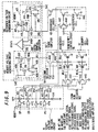
- FIG.9 shows a detailed composition of a specific example of main part in FIG.8.
- the memory cell array 101 is composed of a (m+1) rows x (n+1) columns matrix of memory cells 441, which are flash memory cells.
- the gate voltage from the row decoder 102 is supplied.
- reference numbers 442 and 443 indicate transistors that supply the verify voltage from the verify voltage switching circuit 111 to the word lines WL0 to WLm and are the final stage of the row decoder 102.
- One of bit lines BL0 to BLn is selected by the column selector 104. After all, the output of a memory cell 441 that is full-selected by semi-selected word line and bit line is input to the sense amplifier 107.
- the reference cell array 105 is composed of one reference cell 445 that the threshold voltage is built in accurately, memory cells 446 of number m that the drains are connected to the same line as the reference cell and the gates are grounded, and transistors 447 and 448 that supply the verify voltage from the verify voltage switching circuit 111 to the gate of the reference cell 445. Meanwhile, the m memory cells 446 are provided so that the bit lines BL0 to BLn and the reference line that the reference cell 445 have same floating capacity to improve the reading operation.
- the sense amplifier 107 is composed of a memory voltage generating circuit 431 to convert the output current of the memory cell 441 into voltage on the left side of a differential amplifier 401 and a reference voltage generating circuit 106 to convert the output current of the reference cell 445 into voltage on the right side of the differential amplifier 401.
- the differential amplifier 401 amplifies the voltage difference between the current voltage converter output VDi of the memory voltage generating circuit 431 and the current voltage converter output VREF of the reference voltage generating circuit 106, then outputting it as output DOUT of the sense amplifier.
- a PMOS transistor 417 turns ON, thereby two NMOS transistors 412 are connected in parallel.
- the PMOS transistor 417 turns OFF, thereby the composition of the memory voltage generating circuit 431 becomes equal to that of the reference voltage generating circuit 106, and the sense amplifier 107 becomes symmetrical.
- the reference voltage VREF of the sense amplifier 107 in the normal operation becomes a half of that in the verifying.
- the gate voltages of the memory cell 441 and the reference cell 445 to be equal, in the normal operation, the reference level of the sense amplifier 107 is set to be intermediate between output of memory cell when reading "1" and output of memory cell when reading "0".
- the verifying it is judged whether the threshold of memory cell is higher or lower than a given level. Since the threshold voltage is difficult to measure, current flowing when applying a certain voltage to the gate is compared.
- the full line on the left in FIG.7 is a reference characteristic curve for the erase verify that is set to the reference cell.
- voltage VWref When applying voltage VWref to the gate of the reference cell 445, current IREF flows. Also, when applying voltage VW to the gate of memory cell 441, if the memory cell is at the program verify level, current IREF flows.
- the sense amplifier 107 actuates in response to sense amplifier enabling signal SAE from the timing circuit 108, and parts with reference numbers 420 and 421 are circuits for supplying a low constant voltage to the memory cell array 101 and reference cell array 105.
- the verify voltage switching circuit 111 is composed of four resistors 461 to 464 for dividing the internal high voltage VPP from the high-voltage generating circuit 112 into V 1 , V 2 and V 3 , three NAND gates 471, 472 and 474, an inverter 473, and four PMOS transistors 451 to 454.
- verify signal VERIFY When verify signal VERIFY is enabled, voltage V 2 is supplied to the reference cell array 105 by the inverter 473 and the PMOS transistor 453.
- voltage V 3 is supplied to the memory cell array 101 when program verify signal PG is enabled, voltage V 2 is supplied thereto when erase mode signal ER is enabled, and voltage V 1 is supplied thereto when over-erase mode signal DP is enabled. Namely, in every verify mode, same voltage V 2 is applied to the reference cell array 105, and three kinds of voltage V 1 , V 2 and V 3 are applied to the memory cell array 101 according to the mode. Also, in the erase verify, same voltage V 2 is applied to the memory cell array 101 and the reference cell array 105.
- the threshold voltage of the reference cell 445 is V TM
- V TM 3[V]
- V F program verify level
- V N erase verify level
- the gate voltage V 3 of the reference cell 445 is 1[V] while the gate voltage V 2 of the memory cell 441 is 4[V].
- the difference, 3[V] is equal to the difference between the program verify level, 6[V] and the erase verify level, 3[V]. This is because even for the OFF cell that the most severe programming is conducted and the threshold voltage V F is minimum, it is intended to secure a margin of 3[V] when shifting to ON cell.
- the gate voltage V 2 of the memory cell 441 is 4[V] while the gate voltage V 1 of the reference cell 445 is 6[V].
- the difference is equal to the difference, 2[V] between the erase verify level, 3[V] and the over-erase verify level. 1[V]. This is because it is intended to confirm that the output current from the reference cell 445 is more than the output current all memory cells 441 from ON cell with the threshold voltage at erase verify level of 3[V] equal to the threshold voltage of the reference cell 445 to ON cell with the threshold voltage at over-erase level of 1[V] that is lowered by the width of erase threshold distribution.
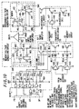
- FIG.10 shows another example.
- the gate voltage of the memory cell 441 is equal to that of the reference cell 445.
- the gate voltage of the memory cell 441 is set higher than that of the reference cell 445 by the difference between the program verify level and the erase verify level.
- the gate voltage of the reference cell 445 is set higher than that of the memory cell 441 by the width of erase threshold distribution.
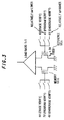
- FIG.3 shows summarizing the second example. Referring to FIG.3 together with FIG.4 that shows the threshold voltage distribution of OFF cell and ON cell, the meaning of the values of gate voltage will be more easily understood.
- circuit composition only of positive voltage is shown, the invention can be applied to a non-volatile semiconductor storage device with positive and negative power sources.
Landscapes
- Read Only Memory (AREA)
- For Increasing The Reliability Of Semiconductor Memories (AREA)
Applications Claiming Priority (2)
| Application Number | Priority Date | Filing Date | Title |
|---|---|---|---|
| JP11659598A JP3346274B2 (ja) | 1998-04-27 | 1998-04-27 | 不揮発性半導体記憶装置 |
| JP11659598 | 1998-04-27 |
Publications (2)
| Publication Number | Publication Date |
|---|---|
| EP0953985A2 true EP0953985A2 (de) | 1999-11-03 |
| EP0953985A3 EP0953985A3 (de) | 2003-08-13 |
Family
ID=14691044
Family Applications (1)
| Application Number | Title | Priority Date | Filing Date |
|---|---|---|---|
| EP99108242A Withdrawn EP0953985A3 (de) | 1998-04-27 | 1999-04-27 | Nichtflüchtige Halbleiterspeicheranordnung |
Country Status (6)
| Country | Link |
|---|---|
| US (1) | US6163484A (de) |
| EP (1) | EP0953985A3 (de) |
| JP (1) | JP3346274B2 (de) |
| KR (1) | KR19990083512A (de) |
| CN (1) | CN1136580C (de) |
| TW (1) | TW422988B (de) |
Cited By (2)
| Publication number | Priority date | Publication date | Assignee | Title |
|---|---|---|---|---|
| WO2002082447A3 (en) * | 2001-04-09 | 2003-03-06 | Advanced Micro Devices Inc | Soft program and soft program verify of the core cells in flash memory array |
| EP1246195A3 (de) * | 2001-03-29 | 2005-08-17 | Fujitsu Limited | Nichtflüchtiger Halbleiterspeicher und Verfahren zur seiner Steuerung |
Families Citing this family (56)
| Publication number | Priority date | Publication date | Assignee | Title |
|---|---|---|---|---|
| US6768165B1 (en) | 1997-08-01 | 2004-07-27 | Saifun Semiconductors Ltd. | Two bit non-volatile electrically erasable and programmable semiconductor memory cell utilizing asymmetrical charge trapping |
| JP3561647B2 (ja) * | 1998-12-10 | 2004-09-02 | 三洋電機株式会社 | 1チップマイクロコンピュータ |
| KR100300549B1 (ko) * | 1999-06-16 | 2001-11-01 | 김영환 | 비휘발성 메모리 센싱장치 및 방법 |
| KR100331549B1 (ko) * | 1999-08-06 | 2002-04-06 | 윤종용 | 더미 비트 라인을 이용한 전류 센스 앰프 회로 |
| KR100322471B1 (ko) * | 1999-10-01 | 2002-02-07 | 윤종용 | 불휘발성 반도체 메모리 장치의 감지 증폭기 회로 |
| JP3420133B2 (ja) | 1999-10-13 | 2003-06-23 | Necエレクトロニクス株式会社 | 半導体記憶装置 |
| JP2001143487A (ja) * | 1999-11-15 | 2001-05-25 | Nec Corp | 半導体記憶装置 |
| US6185143B1 (en) * | 2000-02-04 | 2001-02-06 | Hewlett-Packard Company | Magnetic random access memory (MRAM) device including differential sense amplifiers |
| JP3734408B2 (ja) * | 2000-07-03 | 2006-01-11 | シャープ株式会社 | 半導体記憶装置 |
| JP2002100192A (ja) * | 2000-09-22 | 2002-04-05 | Toshiba Corp | 不揮発性半導体メモリ |
| JP4291505B2 (ja) * | 2000-10-30 | 2009-07-08 | 富士通マイクロエレクトロニクス株式会社 | 半導体記憶装置 |
| US6574145B2 (en) | 2001-03-21 | 2003-06-03 | Matrix Semiconductor, Inc. | Memory device and method for sensing while programming a non-volatile memory cell |
| US6515904B2 (en) | 2001-03-21 | 2003-02-04 | Matrix Semiconductor, Inc. | Method and system for increasing programming bandwidth in a non-volatile memory device |
| US6584017B2 (en) | 2001-04-05 | 2003-06-24 | Saifun Semiconductors Ltd. | Method for programming a reference cell |
| KR20020091581A (ko) * | 2001-05-31 | 2002-12-06 | 삼성전자 주식회사 | 진행성 결함 특성을 갖는 메모리 셀을 검사할 수 있는플래시 메모리 장치 |
| JP2003068094A (ja) * | 2001-08-28 | 2003-03-07 | Mitsubishi Electric Corp | フラッシュメモリ |
| US7057935B2 (en) * | 2001-08-30 | 2006-06-06 | Micron Technology, Inc. | Erase verify for non-volatile memory |
| US6700818B2 (en) | 2002-01-31 | 2004-03-02 | Saifun Semiconductors Ltd. | Method for operating a memory device |
| US6917544B2 (en) | 2002-07-10 | 2005-07-12 | Saifun Semiconductors Ltd. | Multiple use memory chip |
| JP4163473B2 (ja) * | 2002-09-13 | 2008-10-08 | スパンション エルエルシー | 不揮発性半導体記憶装置 |
| US7136304B2 (en) | 2002-10-29 | 2006-11-14 | Saifun Semiconductor Ltd | Method, system and circuit for programming a non-volatile memory array |
| US7178004B2 (en) | 2003-01-31 | 2007-02-13 | Yan Polansky | Memory array programming circuit and a method for using the circuit |
| US7142464B2 (en) * | 2003-04-29 | 2006-11-28 | Saifun Semiconductors Ltd. | Apparatus and methods for multi-level sensing in a memory array |
| US7050346B2 (en) * | 2003-07-29 | 2006-05-23 | Kabushiki Kaisha Toshiba | Non-volatile semiconductor memory device and electric device with the same |
| US7123532B2 (en) | 2003-09-16 | 2006-10-17 | Saifun Semiconductors Ltd. | Operating array cells with matched reference cells |
| JP2005116065A (ja) * | 2003-10-08 | 2005-04-28 | Oki Electric Ind Co Ltd | 不揮発性半導体記憶装置及び読出方法 |
| JP2005141827A (ja) * | 2003-11-06 | 2005-06-02 | Sanyo Electric Co Ltd | 半導体記憶装置およびその不揮発性メモリ検証方法、マイクロコンピュータおよびその不揮発性メモリ制御方法 |
| US7317633B2 (en) | 2004-07-06 | 2008-01-08 | Saifun Semiconductors Ltd | Protection of NROM devices from charge damage |
| US7095655B2 (en) | 2004-08-12 | 2006-08-22 | Saifun Semiconductors Ltd. | Dynamic matching of signal path and reference path for sensing |
| US7638850B2 (en) | 2004-10-14 | 2009-12-29 | Saifun Semiconductors Ltd. | Non-volatile memory structure and method of fabrication |
| US7242618B2 (en) * | 2004-12-09 | 2007-07-10 | Saifun Semiconductors Ltd. | Method for reading non-volatile memory cells |
| US7535765B2 (en) | 2004-12-09 | 2009-05-19 | Saifun Semiconductors Ltd. | Non-volatile memory device and method for reading cells |
| EP1684308A1 (de) | 2005-01-19 | 2006-07-26 | Saifun Semiconductors Ltd. | Verfahren zur Verhinderung von Feststrukturprogrammierung |
| US8053812B2 (en) | 2005-03-17 | 2011-11-08 | Spansion Israel Ltd | Contact in planar NROM technology |
| JP2007027760A (ja) | 2005-07-18 | 2007-02-01 | Saifun Semiconductors Ltd | 高密度不揮発性メモリアレイ及び製造方法 |
| US7668017B2 (en) | 2005-08-17 | 2010-02-23 | Saifun Semiconductors Ltd. | Method of erasing non-volatile memory cells |
| US8116142B2 (en) * | 2005-09-06 | 2012-02-14 | Infineon Technologies Ag | Method and circuit for erasing a non-volatile memory cell |
| US7221138B2 (en) | 2005-09-27 | 2007-05-22 | Saifun Semiconductors Ltd | Method and apparatus for measuring charge pump output current |
| US7352627B2 (en) | 2006-01-03 | 2008-04-01 | Saifon Semiconductors Ltd. | Method, system, and circuit for operating a non-volatile memory array |
| US7808818B2 (en) | 2006-01-12 | 2010-10-05 | Saifun Semiconductors Ltd. | Secondary injection for NROM |
| US7692961B2 (en) | 2006-02-21 | 2010-04-06 | Saifun Semiconductors Ltd. | Method, circuit and device for disturb-control of programming nonvolatile memory cells by hot-hole injection (HHI) and by channel hot-electron (CHE) injection |
| US8253452B2 (en) | 2006-02-21 | 2012-08-28 | Spansion Israel Ltd | Circuit and method for powering up an integrated circuit and an integrated circuit utilizing same |
| US7760554B2 (en) | 2006-02-21 | 2010-07-20 | Saifun Semiconductors Ltd. | NROM non-volatile memory and mode of operation |
| US7638835B2 (en) | 2006-02-28 | 2009-12-29 | Saifun Semiconductors Ltd. | Double density NROM with nitride strips (DDNS) |
| US7701779B2 (en) | 2006-04-27 | 2010-04-20 | Sajfun Semiconductors Ltd. | Method for programming a reference cell |
| US7605579B2 (en) | 2006-09-18 | 2009-10-20 | Saifun Semiconductors Ltd. | Measuring and controlling current consumption and output current of charge pumps |
| JP4911508B2 (ja) * | 2007-03-30 | 2012-04-04 | ルネサスエレクトロニクス株式会社 | 不揮発性半導体記憶装置及びその動作方法 |
| KR100896190B1 (ko) | 2007-06-11 | 2009-05-12 | 삼성전자주식회사 | 불휘발성 메모리 장치의 소거 방법 |
| US8117375B2 (en) * | 2007-10-17 | 2012-02-14 | Micron Technology, Inc. | Memory device program window adjustment |
| JP2009129472A (ja) * | 2007-11-20 | 2009-06-11 | Toshiba Corp | 半導体記憶装置 |
| US7590001B2 (en) | 2007-12-18 | 2009-09-15 | Saifun Semiconductors Ltd. | Flash memory with optimized write sector spares |
| CN101800082B (zh) * | 2009-02-11 | 2012-12-05 | 北京兆易创新科技有限公司 | 一种用于mlc闪存的灵敏放大器和电流电压转换电路 |
| US8406072B2 (en) | 2010-08-23 | 2013-03-26 | Qualcomm Incorporated | System and method of reference cell testing |
| JP5891918B2 (ja) * | 2012-04-11 | 2016-03-23 | 株式会社ソシオネクスト | 不揮発性メモリ、電子装置及び検証方法 |
| JP6846321B2 (ja) * | 2017-09-21 | 2021-03-24 | ルネサスエレクトロニクス株式会社 | 半導体記憶装置、及び半導体記憶装置の制御方法 |
| US10580505B1 (en) * | 2019-02-21 | 2020-03-03 | Elite Semiconductor Memory Technology Inc. | Erasing method used in flash memory |
Family Cites Families (10)
| Publication number | Priority date | Publication date | Assignee | Title |
|---|---|---|---|---|
| JP2853217B2 (ja) * | 1989-11-21 | 1999-02-03 | 日本電気株式会社 | 半導体メモリ |
| JPH0536288A (ja) * | 1991-08-01 | 1993-02-12 | Fujitsu Ltd | 不揮発性半導体記憶装置 |
| US5463586A (en) * | 1993-05-28 | 1995-10-31 | Macronix International Co., Ltd. | Erase and program verification circuit for non-volatile memory |
| US6005805A (en) * | 1994-12-27 | 1999-12-21 | Nkk Corporation | Nonvolatile semiconductor device with a verify function |
| US5629892A (en) * | 1995-10-16 | 1997-05-13 | Advanced Micro Devices, Inc. | Flash EEPROM memory with separate reference array |
| WO2004090908A1 (ja) * | 1996-06-11 | 2004-10-21 | Nobuyoshi Takeuchi | ベリファイ機能を有する不揮発性記憶装置 |
| EP0814484B1 (de) * | 1996-06-18 | 2003-09-17 | STMicroelectronics S.r.l. | Nichtflüchtiger Speicher mit Einzelzellenreferenzsignalgeneratorschaltung zum Auslesen von Speicherzellen |
| DE69702256T2 (de) * | 1996-06-24 | 2001-01-18 | Advanced Micro Devices, Inc. | Verfahren für einen merhfachen, bits pro zelle flash eeprom, speicher mit seitenprogrammierungsmodus und leseverfahren |
| JPH10302486A (ja) * | 1996-08-30 | 1998-11-13 | Sanyo Electric Co Ltd | 半導体記憶装置 |
| US5859796A (en) * | 1997-12-16 | 1999-01-12 | Advanced Micro Devices, Inc. | Programming of memory cells using connected floating gate analog reference cell |
-
1998
- 1998-04-27 JP JP11659598A patent/JP3346274B2/ja not_active Expired - Fee Related
-
1999
- 1999-04-26 US US09/299,021 patent/US6163484A/en not_active Expired - Fee Related
- 1999-04-27 EP EP99108242A patent/EP0953985A3/de not_active Withdrawn
- 1999-04-27 TW TW088106803A patent/TW422988B/zh not_active IP Right Cessation
- 1999-04-27 KR KR1019990014991A patent/KR19990083512A/ko not_active Withdrawn
- 1999-04-27 CN CNB991059999A patent/CN1136580C/zh not_active Expired - Fee Related
Cited By (4)
| Publication number | Priority date | Publication date | Assignee | Title |
|---|---|---|---|---|
| EP1246195A3 (de) * | 2001-03-29 | 2005-08-17 | Fujitsu Limited | Nichtflüchtiger Halbleiterspeicher und Verfahren zur seiner Steuerung |
| WO2002082447A3 (en) * | 2001-04-09 | 2003-03-06 | Advanced Micro Devices Inc | Soft program and soft program verify of the core cells in flash memory array |
| CN100365735C (zh) * | 2001-04-09 | 2008-01-30 | 斯班逊有限公司 | 闪存阵列中核心存储单元的软程序校验的装置和方法 |
| KR100828196B1 (ko) * | 2001-04-09 | 2008-05-08 | 스펜션 엘엘씨 | 플래시 메모리 어레이의 코어 셀들의 소프트 프로그램 및소프트 프로그램 검증 |
Also Published As
| Publication number | Publication date |
|---|---|
| JP3346274B2 (ja) | 2002-11-18 |
| KR19990083512A (ko) | 1999-11-25 |
| TW422988B (en) | 2001-02-21 |
| JPH11306785A (ja) | 1999-11-05 |
| CN1136580C (zh) | 2004-01-28 |
| CN1234585A (zh) | 1999-11-10 |
| EP0953985A3 (de) | 2003-08-13 |
| US6163484A (en) | 2000-12-19 |
Similar Documents
| Publication | Publication Date | Title |
|---|---|---|
| US6163484A (en) | Non-volatile semiconductor storage device having improved program/erase/over erase verify | |
| JP3238574B2 (ja) | 不揮発性半導体記憶装置とその消去方法 | |
| US6097638A (en) | Semiconductor memory device | |
| US8339852B2 (en) | Non-volatile memory device | |
| US5661685A (en) | Programmable logic device with configurable power supply | |
| US6411549B1 (en) | Reference cell for high speed sensing in non-volatile memories | |
| US4841482A (en) | Leakage verification for flash EPROM | |
| US5544116A (en) | Erase and program verification circuit for non-volatile memory | |
| EP0251429B1 (de) | Nichtflüchtiger Halbleiterspeicher | |
| EP0241327B1 (de) | Leseverstärker für programmierbaren Festwertspeicher | |
| US20090231915A1 (en) | Reading array cell with matched reference cell | |
| JPH07192478A (ja) | メモリアレイ内のメモリセルによって記憶される複数個の可能な状態における1つの状態を定めるための基準、メモリ、アレイセルのしきい値電圧を読出すのに用いられる複数個の基準セルをプログラムするための装置、n個の基準セルをプログラムする方法、およびアレイセルを読出す方法 | |
| US6580644B1 (en) | Flash memory device capable of checking memory cells for failure characteristics | |
| JPH06176585A (ja) | 半導体記憶装置 | |
| KR100433435B1 (ko) | 반도체메모리 | |
| US6999345B1 (en) | Method of sense and program verify without a reference cell for non-volatile semiconductor memory | |
| JP3318929B2 (ja) | 不揮発性半導体装置 | |
| US7872918B2 (en) | Nonvolatile memory device and program or erase method using the same | |
| US6400608B1 (en) | Accurate verify apparatus and method for NOR flash memory cells in the presence of high column leakage | |
| EP0862184B1 (de) | Halbleiterspeicheranordnung mit der Fähigkeit, genaue und gemeinsame Löschprüfung von allen Speicherzellen auszuführen | |
| US6987703B2 (en) | Nonvolatile semiconductor storage device and write time determining method therefor | |
| KR20070065776A (ko) | 불휘발성 반도체 메모리 장치 | |
| JP3176011B2 (ja) | 半導体記憶装置 | |
| JP2000057783A (ja) | 不揮発性半導体メモリ | |
| US6324108B1 (en) | Application of external voltage during array VT testing |
Legal Events
| Date | Code | Title | Description |
|---|---|---|---|
| PUAI | Public reference made under article 153(3) epc to a published international application that has entered the european phase |
Free format text: ORIGINAL CODE: 0009012 |
|
| AK | Designated contracting states |
Kind code of ref document: A2 Designated state(s): AT BE CH CY DE DK ES FI FR GB GR IE IT LI LU MC NL PT SE |
|
| AX | Request for extension of the european patent |
Free format text: AL;LT;LV;MK;RO;SI |
|
| RAP1 | Party data changed (applicant data changed or rights of an application transferred) |
Owner name: NEC ELECTRONICS CORPORATION |
|
| PUAL | Search report despatched |
Free format text: ORIGINAL CODE: 0009013 |
|
| AK | Designated contracting states |
Designated state(s): AT BE CH CY DE DK ES FI FR GB GR IE IT LI LU MC NL PT SE |
|
| AX | Request for extension of the european patent |
Extension state: AL LT LV MK RO SI |
|
| RIC1 | Information provided on ipc code assigned before grant |
Ipc: 7G 11C 16/34 B Ipc: 7G 11C 16/06 A |
|
| 17P | Request for examination filed |
Effective date: 20030709 |
|
| AKX | Designation fees paid |
Designated state(s): DE FR IT |
|
| 17Q | First examination report despatched |
Effective date: 20040608 |
|
| STAA | Information on the status of an ep patent application or granted ep patent |
Free format text: STATUS: THE APPLICATION HAS BEEN WITHDRAWN |
|
| 18W | Application withdrawn |
Effective date: 20040817 |