EP0971405A2 - Procédé pour la fabrication d'un substrat por un "stud grid array" en polymère - Google Patents
Procédé pour la fabrication d'un substrat por un "stud grid array" en polymère Download PDFInfo
- Publication number
- EP0971405A2 EP0971405A2 EP99116980A EP99116980A EP0971405A2 EP 0971405 A2 EP0971405 A2 EP 0971405A2 EP 99116980 A EP99116980 A EP 99116980A EP 99116980 A EP99116980 A EP 99116980A EP 0971405 A2 EP0971405 A2 EP 0971405A2
- Authority
- EP
- European Patent Office
- Prior art keywords
- substrate
- connections
- chip
- polymer
- der
- Prior art date
- Legal status (The legal status is an assumption and is not a legal conclusion. Google has not performed a legal analysis and makes no representation as to the accuracy of the status listed.)
- Withdrawn
Links
Images


Classifications
-
- H—ELECTRICITY
- H05—ELECTRIC TECHNIQUES NOT OTHERWISE PROVIDED FOR
- H05K—PRINTED CIRCUITS; CASINGS OR CONSTRUCTIONAL DETAILS OF ELECTRIC APPARATUS; MANUFACTURE OF ASSEMBLAGES OF ELECTRICAL COMPONENTS
- H05K3/00—Apparatus or processes for manufacturing printed circuits
- H05K3/40—Forming printed elements for providing electric connections to or between printed circuits
- H05K3/4007—Surface contacts, e.g. bumps
-
- H—ELECTRICITY
- H10—SEMICONDUCTOR DEVICES; ELECTRIC SOLID-STATE DEVICES NOT OTHERWISE PROVIDED FOR
- H10W—GENERIC PACKAGES, INTERCONNECTIONS, CONNECTORS OR OTHER CONSTRUCTIONAL DETAILS OF DEVICES COVERED BY CLASS H10
- H10W70/00—Package substrates; Interposers; Redistribution layers [RDL]
- H10W70/60—Insulating or insulated package substrates; Interposers; Redistribution layers
-
- H—ELECTRICITY
- H10—SEMICONDUCTOR DEVICES; ELECTRIC SOLID-STATE DEVICES NOT OTHERWISE PROVIDED FOR
- H10W—GENERIC PACKAGES, INTERCONNECTIONS, CONNECTORS OR OTHER CONSTRUCTIONAL DETAILS OF DEVICES COVERED BY CLASS H10
- H10W70/00—Package substrates; Interposers; Redistribution layers [RDL]
- H10W70/60—Insulating or insulated package substrates; Interposers; Redistribution layers
- H10W70/67—Insulating or insulated package substrates; Interposers; Redistribution layers characterised by their insulating layers or insulating parts
- H10W70/68—Shapes or dispositions thereof
-
- H—ELECTRICITY
- H10—SEMICONDUCTOR DEVICES; ELECTRIC SOLID-STATE DEVICES NOT OTHERWISE PROVIDED FOR
- H10W—GENERIC PACKAGES, INTERCONNECTIONS, CONNECTORS OR OTHER CONSTRUCTIONAL DETAILS OF DEVICES COVERED BY CLASS H10
- H10W90/00—Package configurations
- H10W90/701—Package configurations characterised by the relative positions of pads or connectors relative to package parts
-
- B—PERFORMING OPERATIONS; TRANSPORTING
- B29—WORKING OF PLASTICS; WORKING OF SUBSTANCES IN A PLASTIC STATE IN GENERAL
- B29L—INDEXING SCHEME ASSOCIATED WITH SUBCLASS B29C, RELATING TO PARTICULAR ARTICLES
- B29L2031/00—Other particular articles
- B29L2031/34—Electrical apparatus, e.g. sparking plugs or parts thereof
- B29L2031/3493—Moulded interconnect devices, i.e. moulded articles provided with integrated circuit traces
-
- H—ELECTRICITY
- H05—ELECTRIC TECHNIQUES NOT OTHERWISE PROVIDED FOR
- H05K—PRINTED CIRCUITS; CASINGS OR CONSTRUCTIONAL DETAILS OF ELECTRIC APPARATUS; MANUFACTURE OF ASSEMBLAGES OF ELECTRICAL COMPONENTS
- H05K2201/00—Indexing scheme relating to printed circuits covered by H05K1/00
- H05K2201/03—Conductive materials
- H05K2201/0332—Structure of the conductor
- H05K2201/0364—Conductor shape
- H05K2201/0367—Metallic bump or raised conductor not used as solder bump
-
- H—ELECTRICITY
- H05—ELECTRIC TECHNIQUES NOT OTHERWISE PROVIDED FOR
- H05K—PRINTED CIRCUITS; CASINGS OR CONSTRUCTIONAL DETAILS OF ELECTRIC APPARATUS; MANUFACTURE OF ASSEMBLAGES OF ELECTRICAL COMPONENTS
- H05K2201/00—Indexing scheme relating to printed circuits covered by H05K1/00
- H05K2201/09—Shape and layout
- H05K2201/09009—Substrate related
- H05K2201/09045—Locally raised area or protrusion of insulating substrate
-
- H—ELECTRICITY
- H05—ELECTRIC TECHNIQUES NOT OTHERWISE PROVIDED FOR
- H05K—PRINTED CIRCUITS; CASINGS OR CONSTRUCTIONAL DETAILS OF ELECTRIC APPARATUS; MANUFACTURE OF ASSEMBLAGES OF ELECTRICAL COMPONENTS
- H05K2201/00—Indexing scheme relating to printed circuits covered by H05K1/00
- H05K2201/09—Shape and layout
- H05K2201/09009—Substrate related
- H05K2201/09118—Moulded substrate
-
- H—ELECTRICITY
- H05—ELECTRIC TECHNIQUES NOT OTHERWISE PROVIDED FOR
- H05K—PRINTED CIRCUITS; CASINGS OR CONSTRUCTIONAL DETAILS OF ELECTRIC APPARATUS; MANUFACTURE OF ASSEMBLAGES OF ELECTRICAL COMPONENTS
- H05K3/00—Apparatus or processes for manufacturing printed circuits
- H05K3/02—Apparatus or processes for manufacturing printed circuits in which the conductive material is applied to the surface of the insulating support and is thereafter removed from such areas of the surface which are not intended for current conducting or shielding
- H05K3/027—Apparatus or processes for manufacturing printed circuits in which the conductive material is applied to the surface of the insulating support and is thereafter removed from such areas of the surface which are not intended for current conducting or shielding the conductive material being removed by irradiation, e.g. by photons, alpha or beta particles
-
- H—ELECTRICITY
- H05—ELECTRIC TECHNIQUES NOT OTHERWISE PROVIDED FOR
- H05K—PRINTED CIRCUITS; CASINGS OR CONSTRUCTIONAL DETAILS OF ELECTRIC APPARATUS; MANUFACTURE OF ASSEMBLAGES OF ELECTRICAL COMPONENTS
- H05K3/00—Apparatus or processes for manufacturing printed circuits
- H05K3/30—Assembling printed circuits with electric components, e.g. with resistors
- H05K3/32—Assembling printed circuits with electric components, e.g. with resistors electrically connecting electric components or wires to printed circuits
- H05K3/34—Assembling printed circuits with electric components, e.g. with resistors electrically connecting electric components or wires to printed circuits by soldering
- H05K3/341—Surface mounted components
- H05K3/3431—Leadless components
-
- H—ELECTRICITY
- H10—SEMICONDUCTOR DEVICES; ELECTRIC SOLID-STATE DEVICES NOT OTHERWISE PROVIDED FOR
- H10W—GENERIC PACKAGES, INTERCONNECTIONS, CONNECTORS OR OTHER CONSTRUCTIONAL DETAILS OF DEVICES COVERED BY CLASS H10
- H10W70/00—Package substrates; Interposers; Redistribution layers [RDL]
- H10W70/60—Insulating or insulated package substrates; Interposers; Redistribution layers
- H10W70/67—Insulating or insulated package substrates; Interposers; Redistribution layers characterised by their insulating layers or insulating parts
- H10W70/68—Shapes or dispositions thereof
- H10W70/682—Shapes or dispositions thereof comprising holes having chips therein
-
- H—ELECTRICITY
- H10—SEMICONDUCTOR DEVICES; ELECTRIC SOLID-STATE DEVICES NOT OTHERWISE PROVIDED FOR
- H10W—GENERIC PACKAGES, INTERCONNECTIONS, CONNECTORS OR OTHER CONSTRUCTIONAL DETAILS OF DEVICES COVERED BY CLASS H10
- H10W72/00—Interconnections or connectors in packages
- H10W72/071—Connecting or disconnecting
- H10W72/072—Connecting or disconnecting of bump connectors
- H10W72/07231—Techniques
- H10W72/07236—Soldering or alloying
-
- H—ELECTRICITY
- H10—SEMICONDUCTOR DEVICES; ELECTRIC SOLID-STATE DEVICES NOT OTHERWISE PROVIDED FOR
- H10W—GENERIC PACKAGES, INTERCONNECTIONS, CONNECTORS OR OTHER CONSTRUCTIONAL DETAILS OF DEVICES COVERED BY CLASS H10
- H10W72/00—Interconnections or connectors in packages
- H10W72/071—Connecting or disconnecting
- H10W72/072—Connecting or disconnecting of bump connectors
- H10W72/07251—Connecting or disconnecting of bump connectors characterised by changes in properties of the bump connectors during connecting
-
- H—ELECTRICITY
- H10—SEMICONDUCTOR DEVICES; ELECTRIC SOLID-STATE DEVICES NOT OTHERWISE PROVIDED FOR
- H10W—GENERIC PACKAGES, INTERCONNECTIONS, CONNECTORS OR OTHER CONSTRUCTIONAL DETAILS OF DEVICES COVERED BY CLASS H10
- H10W72/00—Interconnections or connectors in packages
- H10W72/20—Bump connectors, e.g. solder bumps or copper pillars; Dummy bumps; Thermal bumps
-
- H—ELECTRICITY
- H10—SEMICONDUCTOR DEVICES; ELECTRIC SOLID-STATE DEVICES NOT OTHERWISE PROVIDED FOR
- H10W—GENERIC PACKAGES, INTERCONNECTIONS, CONNECTORS OR OTHER CONSTRUCTIONAL DETAILS OF DEVICES COVERED BY CLASS H10
- H10W72/00—Interconnections or connectors in packages
- H10W72/20—Bump connectors, e.g. solder bumps or copper pillars; Dummy bumps; Thermal bumps
- H10W72/251—Materials
- H10W72/253—Materials not comprising solid metals or solid metalloids, e.g. polymers or ceramics
-
- H—ELECTRICITY
- H10—SEMICONDUCTOR DEVICES; ELECTRIC SOLID-STATE DEVICES NOT OTHERWISE PROVIDED FOR
- H10W—GENERIC PACKAGES, INTERCONNECTIONS, CONNECTORS OR OTHER CONSTRUCTIONAL DETAILS OF DEVICES COVERED BY CLASS H10
- H10W74/00—Encapsulations, e.g. protective coatings
Definitions
- Integrated circuits are getting more and more connections and are miniaturized more and more.
- the one at this increasing miniaturization expected difficulties with Solder paste application and assembly, should be due to new housing shapes to be remedied, in particular single few or Highlight multi-chip modules in the Ball Grid Array Package are (DE-Z productronic 5, 1994, pages 54, 55).
- This Modules are based on a plated-through substrate which the chips for example via contact wires or are contacted by means of flip chip assembly.
- the substrate On the bottom the substrate is the Ball Grid Array (BGA), the often as a Solder Grid Array, Land Grid Array or Solder Bump array.
- the ball grid array includes solder bumps arranged flat on the underside of the substrate, which is a surface mount on the circuit boards or enable modules. Due to the flat arrangement of the Solder bumps can have large numbers of connections in a rough grid of, for example, 1.27 mm.
- MID M oulded I nterconnection D evices
- injection-molded parts are used with integrated conductor tracks instead of conventional printed circuits.
- High-quality thermoplastics that are suitable for injection molding three-dimensional substrates are the basis of this technology.
- Thermoplastics of this type are distinguished from conventional substrate materials for printed circuits by better mechanical, thermal, chemical, electrical and environmental properties.
- SIL S injection-molded parts with i ntegr faced L pus-trains
- the structuring is a layer applied to the molded parts metal layer, dispensing with the usual mask technique using a special laser patterning method.
- the housing support function takes over guides and snap connections at the same time, while the metallization layer serves not only as a wiring and connection function but also as an electromagnetic shield and ensures good heat dissipation. Further details on the production of three-dimensional injection molded parts with integrated conductor tracks can be found, for example, in DE-A-37 32 249 or EP-A-0 361 192.
- From US-A-5 081 520 is a method for attaching IC chips known on substrates, in which the substrates as injection molded parts with integrated bumps for fastening of the IC chips are manufactured. After metallizing a connection layer is applied to the bump so that the IC chips can be attached to the substrates, whereby the chip pads with the associated metallizations the hump can be electrically connected.
- the invention specified in claim 1 is based on the problem specify a method for producing a substrate, with which a new design for single, Few or Multi-chip modules can be realized which have the advantages the MID technology and a flat arrangement of the External connections, as is possible with the Ball Grid Array.
- the new design is based on the Ball Grid Array (BGA) referred to as Polymer Stud Grid Array (PSGA), where the term "polymer stud" to that when injection molding the substrate molded polymer bump should indicate.
- BGA Ball Grid Array
- PSGA Polymer Stud Grid Array
- the manufacture can also the external connections on the polymer bumps with minimal effort together with that for MID technology or SIL technology usual production of the conductor tracks are made. Due to the laser fine structuring preferred in the SIL technique, can the external connections on the polymer bumps with high numbers of connections in a very fine Grid can be realized. It should also be emphasized that the Temperature expansion of the polymer bumps the temperature expansion of the substrate and the circuit board receiving the module corresponds.
- the polymer bumps enable through their elastic properties at least a partial compensation.
- the Dimensional stability of the external connections formed on the polymer bumps can also provide security for repairs and replacements opposite the ball grid arrays with their through solder bumps formed external connections can be increased significantly.
- the embodiment according to claim 2 enables flexible Use of the substrate for single, Few or multi-chip modules.
- the configurations according to claims 3 and 4 enable a sunken assembly of the chips in wells of the injection molded Substrates, resulting in an extremely small thickness of the resulting Single, Few or multi-chip modules implemented can be.
- the sunken mounting also allows one optimal protection of the chips, as well as a simple and hermetic sealed encapsulation.
- Figure 1 shows a section through part of a polymer Stud grid arrays contacted with a wire bond technique Chip C1.
- the basis of the array shown is a substrate S, that with "polymer studs" or polymer bumps PS and a trough M1 is provided, the trough M1 being labeled ST Level.
- the production of the substrate S including polymer bumps PS, M1 and ST level by injection molding, using high temperature resistant substrate materials
- Thermoplastics such as polyetherimide, polyether sulfone or liquid crystalline polymers are suitable.
- the substrate S shown in Figure 1 is corresponding to the MID technology completely metallized and then a laser structuring process subjected, as a result this laser structuring external connections AA on the polymer bumps PS, internal connections IA1 at level ST and themselves conductor tracks LZ extending in between remain.
- the external connections AA are in the tip area with a solder layer LS provided, this solder layer LS, for example, by a Tin-lead alloy is formed.
- the solder layer LS can also be, for example, one of a layer sequence of Nickel and gold existing solderable end surface is provided his.
- the internal connections IA1 arranged on the stage ST are connected via contacts KD to the connections CA1 of the am Bottom of the trough M1 connected in face-up position to attached chips C1.
- Figure 2 shows a section through part of a polymer Stud grid arrays with one according to a first embodiment Chip C2 contacted using flip-chip technology.
- FIG. 1 shows the internal connections labeled IA2 at the bottom of a trough designated M2.
- the face down position Chip C2 arranged in the depression M2 has chip connections CA2 in the form of fusible cusps that are assigned to the Internal connections IA2 rest and with these at Soldering.
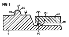
- Figure 3 shows a section through part of a polymer Stud grid arrays with one according to a second embodiment Chip C3 contacted using flip-chip technology.
- the difference for Figures 1 and 2 are those designated here with IA3 Internal connections through additional injection molding of the Substrate S formed in the bottom area of the recess M3 and with a polymer bump PH provided with a solderable end surface.
- the polymer bumps PH for the internal connections IA3 have about a third of the volume of the polymer bumps PS for the external connections AA.
- the face down position in the hollow M3 arranged C3, lies with its chip connections CA3 on the assigned internal connections IA3 of the polymer bumps PH on and is connected to this by soldering.
- the solder not shown here, can be in the form, for example one in the tip area on the internal connections IA3 Solder layer are provided, in the same way, as with the external connections AA.
- Figures 4 and 5 show details of that shown in Figure 1 Polymer Stud Grid Arrays, with the substrate S here however, before mounting the chip C1 in the recess M1 has been. It can be seen that the on the polymer bumps PS formed external connections AA in rows fine grid can be arranged.
- the MID technology Usual laser fine structuring also enables arrangement of the LZ and the internal connections IA1 located at level ST.
- FIGS. 1 to 5 show the principle of a polymer stud grid Arrays with external connections formed on polymer bumps. Deviating from the shape shown in the drawing the polymer bumps also have other shapes, e.g. a truncated cone shape exhibit. Although only one chip is shown at a time the new design can be used for single, Few or multi-chip modules be applied. The chips can also, for example by pouring out the troughs or by attaching them are encapsulated by lids. On the top and the side surfaces of the injection molded substrate can also a metallization layer as an electromagnetic shield or remain for good heat dissipation.
- the substrate with vias, and to arrange a second wiring layer on the top.
- this second wiring layer after the Application of appropriate dielectric layers also more Conductor levels formed in the manner of multi-layer wiring become.
- the polymer bumps and the chip or the chips arranged on different sides of the substrate his.
- Such an arrangement of polymer bumps and Chips on opposite sides of the substrate is special for large chips that have a variety of associated Need external connections, interesting.
Landscapes
- Engineering & Computer Science (AREA)
- Manufacturing & Machinery (AREA)
- Microelectronics & Electronic Packaging (AREA)
- Injection Moulding Of Plastics Or The Like (AREA)
- Encapsulation Of And Coatings For Semiconductor Or Solid State Devices (AREA)
- Wire Bonding (AREA)
- Insulators (AREA)
- Analysing Materials By The Use Of Radiation (AREA)
- Prostheses (AREA)
- Structures Or Materials For Encapsulating Or Coating Semiconductor Devices Or Solid State Devices (AREA)
- Road Signs Or Road Markings (AREA)
- Measurement Of Radiation (AREA)
- Hybrid Cells (AREA)
Applications Claiming Priority (3)
| Application Number | Priority Date | Filing Date | Title |
|---|---|---|---|
| DE4434086 | 1994-09-23 | ||
| DE4434086 | 1994-09-23 | ||
| EP95934106A EP0782765B1 (fr) | 1994-09-23 | 1995-09-22 | Emballage de matrice a projections en polymeres |
Related Parent Applications (2)
| Application Number | Title | Priority Date | Filing Date |
|---|---|---|---|
| EP95934106A Division EP0782765B1 (fr) | 1994-09-23 | 1995-09-22 | Emballage de matrice a projections en polymeres |
| EP95934106.6 Division | 1996-05-10 |
Publications (2)
| Publication Number | Publication Date |
|---|---|
| EP0971405A2 true EP0971405A2 (fr) | 2000-01-12 |
| EP0971405A3 EP0971405A3 (fr) | 2000-05-10 |
Family
ID=6529054
Family Applications (2)
| Application Number | Title | Priority Date | Filing Date |
|---|---|---|---|
| EP99116980A Withdrawn EP0971405A3 (fr) | 1994-09-23 | 1995-09-22 | Procédé pour la fabrication d'un substrat por un "stud grid array" en polymère |
| EP95934106A Expired - Lifetime EP0782765B1 (fr) | 1994-09-23 | 1995-09-22 | Emballage de matrice a projections en polymeres |
Family Applications After (1)
| Application Number | Title | Priority Date | Filing Date |
|---|---|---|---|
| EP95934106A Expired - Lifetime EP0782765B1 (fr) | 1994-09-23 | 1995-09-22 | Emballage de matrice a projections en polymeres |
Country Status (10)
| Country | Link |
|---|---|
| US (1) | US5929516A (fr) |
| EP (2) | EP0971405A3 (fr) |
| JP (2) | JP3112949B2 (fr) |
| KR (1) | KR100279196B1 (fr) |
| AT (1) | ATE194249T1 (fr) |
| DE (1) | DE59508519D1 (fr) |
| DK (1) | DK0782765T3 (fr) |
| ES (1) | ES2148564T3 (fr) |
| PT (1) | PT782765E (fr) |
| WO (1) | WO1996009646A1 (fr) |
Cited By (3)
| Publication number | Priority date | Publication date | Assignee | Title |
|---|---|---|---|---|
| DE10145348C1 (de) * | 2001-09-14 | 2003-03-27 | Siemens Dematic Ag | Zwischenträger für elektronische Bauelemente und Verfahren zur Lötkontaktierung eines derartigen Zwischenträgers |
| DE10202145A1 (de) * | 2002-01-21 | 2003-05-08 | Siemens Dematic Ag | Verfahren zur Herstellung von Anschlußsubstraten für elektronische Bauelemente |
| WO2003105222A1 (fr) * | 2002-06-07 | 2003-12-18 | Siemens Dematic Ag | Procede pour etablir le contact par raccords de composants electroniques sur un substrat isolant et module composant fabrique selon ce procede |
Families Citing this family (62)
| Publication number | Priority date | Publication date | Assignee | Title |
|---|---|---|---|---|
| JP2794678B2 (ja) | 1991-08-26 | 1998-09-10 | 株式会社 半導体エネルギー研究所 | 絶縁ゲイト型半導体装置およびその作製方法 |
| US6249048B1 (en) * | 1997-03-21 | 2001-06-19 | Siemens N.V. | Polymer stud grid array |
| ES2170272T3 (es) * | 1995-10-16 | 2002-08-01 | Siemens Nv | Carcasa de matriz de protuberancias polimeras para sistemas de conexiones de microondas. |
| JP3037440B2 (ja) * | 1995-10-16 | 2000-04-24 | シーメンス エヌ フェー | ポリマースタッド−グリッドアレイ |
| US6072239A (en) | 1995-11-08 | 2000-06-06 | Fujitsu Limited | Device having resin package with projections |
| US6159770A (en) * | 1995-11-08 | 2000-12-12 | Fujitsu Limited | Method and apparatus for fabricating semiconductor device |
| US6329711B1 (en) | 1995-11-08 | 2001-12-11 | Fujitsu Limited | Semiconductor device and mounting structure |
| US6376921B1 (en) | 1995-11-08 | 2002-04-23 | Fujitsu Limited | Semiconductor device, method for fabricating the semiconductor device, lead frame and method for producing the lead frame |
| JPH10135613A (ja) * | 1996-10-28 | 1998-05-22 | Ngk Spark Plug Co Ltd | 配線基板 |
| US6040618A (en) | 1997-03-06 | 2000-03-21 | Micron Technology, Inc. | Multi-chip module employing a carrier substrate with micromachined alignment structures and method of forming |
| JP2934202B2 (ja) * | 1997-03-06 | 1999-08-16 | 山一電機株式会社 | 配線基板における導電バンプの形成方法 |
| EP0968631B1 (fr) * | 1997-03-11 | 2001-11-28 | Siemens S.A. | Procede de formation de circuits metalliques conducteurs sur des supports electriquement isolants |
| TW411741B (en) * | 1997-08-22 | 2000-11-11 | Siemens Ag | Method to produce a conductive transverse-connection between two wiring-areas on a substrate |
| DE69807406T2 (de) | 1997-10-01 | 2003-04-24 | Nippon Shokubai Co. Ltd., Osaka | Verfahren zur Herstellung von Alkylamino-(meth)Acrylat und eine Vorrichtung dafür |
| JP3097653B2 (ja) | 1998-04-17 | 2000-10-10 | 日本電気株式会社 | 半導体装置用パッケージおよびその製造方法 |
| WO1999063589A1 (fr) * | 1998-06-02 | 1999-12-09 | Siemens S.A. | Groupement de plages de connexion disposees en grille et procede de realisation d'un tel groupement |
| TW420853B (en) * | 1998-07-10 | 2001-02-01 | Siemens Ag | Method of manufacturing the wiring with electric conducting interconnect between the over-side and the underside of the substrate and the wiring with such interconnect |
| FR2781309B1 (fr) * | 1998-07-15 | 2001-10-26 | Rue Cartes Et Systemes De | Procede d'assemblage d'un microcircuit sur un support plastique |
| EP1161700A2 (fr) | 1999-03-16 | 2001-12-12 | Framatome Connectors International | Connecteur optoelectronique modulaire |
| WO2000072378A1 (fr) * | 1999-05-20 | 2000-11-30 | Siemens Aktiengesellschaft | Substrat comportant au moins deux saillies de polymere metallisees pour connexion par brasage avec un cablage |
| ATE257103T1 (de) | 1999-11-22 | 2004-01-15 | Hirschmann Austria Gmbh | Zünder |
| DE10025774A1 (de) * | 2000-05-26 | 2001-12-06 | Osram Opto Semiconductors Gmbh | Halbleiterbauelement mit Oberflächenmetallisierung |
| DE10037292A1 (de) * | 2000-07-31 | 2002-02-21 | Siemens Ag | Verfahren zur Herstellung von Anschlußsubstraten für Halbleiterkomponenten |
| DE10048489C1 (de) * | 2000-09-29 | 2002-08-08 | Siemens Ag | Polymer Stud Grid Array und Verfahren zur Herstellung eines derartigen Polymer Stud Grid Arrays |
| US6872591B1 (en) | 2000-10-13 | 2005-03-29 | Bridge Semiconductor Corporation | Method of making a semiconductor chip assembly with a conductive trace and a substrate |
| US6876072B1 (en) | 2000-10-13 | 2005-04-05 | Bridge Semiconductor Corporation | Semiconductor chip assembly with chip in substrate cavity |
| DE10059176C2 (de) * | 2000-11-29 | 2002-10-24 | Siemens Ag | Zwischenträger für ein Halbleitermodul, unter Verwendung eines derartigen Zwischenträgers hergestelltes Halbleitermodul sowie Verfahren zur Herstellung eines derartigen Halbleitermoduls |
| DE10059178C2 (de) * | 2000-11-29 | 2002-11-07 | Siemens Production & Logistics | Verfahren zur Herstellung von Halbleitermodulen sowie nach dem Verfahren hergestelltes Modul |
| DE10062386A1 (de) * | 2000-12-14 | 2002-07-04 | Siemens Production & Logistics | Zwischenträger für ein Halbleitermodul sowie Anordnung eines mit einem solchen Zwischenträger gebildeten Moduls auf einem Schaltungsträger |
| US6444489B1 (en) | 2000-12-15 | 2002-09-03 | Charles W. C. Lin | Semiconductor chip assembly with bumped molded substrate |
| DE10163799B4 (de) * | 2000-12-28 | 2006-11-23 | Matsushita Electric Works, Ltd., Kadoma | Halbleiterchip-Aufbausubstrat und Verfahren zum Herstellen eines solchen Aufbausubstrates |
| JP4604387B2 (ja) * | 2001-04-24 | 2011-01-05 | パナソニック電工株式会社 | Ic実装用基板 |
| DE10120256C1 (de) | 2001-04-25 | 2002-11-28 | Siemens Production & Logistics | Anschlußgehäuse für ein elektronisches Bauelement |
| US6717126B1 (en) | 2001-07-16 | 2004-04-06 | Amkor Technology, Inc. | Method of fabricating and using an image sensor package with reflector |
| US6686580B1 (en) | 2001-07-16 | 2004-02-03 | Amkor Technology, Inc. | Image sensor package with reflector |
| DE10143520A1 (de) * | 2001-09-05 | 2003-04-03 | Siemens Dematic Ag | Lösung und Verfahren zum Bearbeiten der Oberfläche von Kunststoffen, insbesondere von LCP-Substraten zur Verbesserung der Haftung von Metallisierungen und Verwendung einer derartigen Lösung |
| US6486549B1 (en) | 2001-11-10 | 2002-11-26 | Bridge Semiconductor Corporation | Semiconductor module with encapsulant base |
| US6666693B2 (en) | 2001-11-20 | 2003-12-23 | Fci Americas Technology, Inc. | Surface-mounted right-angle electrical connector |
| US6638082B2 (en) | 2001-11-20 | 2003-10-28 | Fci Americas Technology, Inc. | Pin-grid-array electrical connector |
| DE10201643A1 (de) * | 2002-01-17 | 2003-05-08 | Siemens Dematic Ag | Anschlußträger für ein elektronisches Bauelement und unter Verwendung eines derartigen Anschlußträgers gebildetes Bauelement-Modul |
| GB2387714A (en) * | 2002-04-19 | 2003-10-22 | Denselight Semiconductors Pte | Mount for a semiconductor device |
| DE10217698B4 (de) * | 2002-04-20 | 2008-04-24 | Festo Ag & Co. | Elektrische Schaltanordnung mit einem spritzgegossenen Schaltungsträger |
| DE10217700A1 (de) * | 2002-04-20 | 2003-11-06 | Festo Ag & Co | Spritzgegossener Schaltungsträger und damit ausgestattete elektrische Schaltungsanordnung |
| DE10223203B4 (de) * | 2002-05-24 | 2004-04-01 | Siemens Dematic Ag | Elektronisches Bauelement-Modul und Verfahren zu dessen Herstellung |
| DE10227305A1 (de) * | 2002-06-19 | 2003-09-04 | Siemens Dematic Ag | Elektrisches Mehrschicht-Bauelement-Modul und Verfahren zu dessen Herstellung |
| EP1383360B1 (fr) | 2002-07-18 | 2007-01-03 | FESTO AG & Co | Support de circuit imprimé moulé par injection et son procédé de fabrication |
| DE10308095B3 (de) * | 2003-02-24 | 2004-10-14 | Infineon Technologies Ag | Elektronisches Bauteil mit mindestens einem Halbleiterchip auf einem Schaltungsträger und Verfahren zur Herstellung desselben |
| US7052763B2 (en) * | 2003-08-05 | 2006-05-30 | Xerox Corporation | Multi-element connector |
| US20050031840A1 (en) * | 2003-08-05 | 2005-02-10 | Xerox Corporation | RF connector |
| DE10355921B4 (de) * | 2003-11-29 | 2005-12-22 | Festo Ag & Co. | Elektrische Schaltungsanordnung mit einem elektronischen Chip in einer Aufnahmevorrichtung des Schaltungsträgers |
| DE102004026596A1 (de) * | 2004-06-01 | 2006-03-02 | eupec Europäische Gesellschaft für Leistungshalbleiter mbH | Leistungshalbleiteranordnung |
| DE102004035284B4 (de) * | 2004-07-21 | 2008-10-02 | Festo Ag & Co. Kg | Positionssensoranordnung mit mehreren in einer Reihe angeordneten, magnetfeldsensitiven Sensoren, insbesondere Hall-Sensoren |
| US20070109756A1 (en) * | 2005-02-10 | 2007-05-17 | Stats Chippac Ltd. | Stacked integrated circuits package system |
| DE102005046008B4 (de) * | 2005-09-26 | 2007-05-24 | Infineon Technologies Ag | Halbleitersensorbauteil mit Sensorchip und Verfahren zur Herstellung desselben |
| US7928582B2 (en) * | 2007-03-09 | 2011-04-19 | Micron Technology, Inc. | Microelectronic workpieces and methods for manufacturing microelectronic devices using such workpieces |
| JP5221315B2 (ja) * | 2008-12-17 | 2013-06-26 | 新光電気工業株式会社 | 配線基板及びその製造方法 |
| US8974869B2 (en) * | 2010-01-26 | 2015-03-10 | Robert Hamilton | Method for improving plating on non-conductive substrates |
| DE102011109006A1 (de) * | 2011-07-29 | 2013-01-31 | Epcos Ag | Gehäuse für einen Halbleiterchip und Halbleiterchip mit einem Gehäuse |
| DE102014206608A1 (de) * | 2014-04-04 | 2015-10-08 | Siemens Aktiengesellschaft | Verfahren zum Montieren eines elektrischen Bauelements, bei der eine Haube zum Einsatz kommt, und zur Anwendung in diesem Verfahren geeignete Haube |
| DE102014206601A1 (de) * | 2014-04-04 | 2015-10-08 | Siemens Aktiengesellschaft | Verfahren zum Montieren eines elektrischen Bauelements, bei der eine Haube zum Einsatz kommt, und zur Anwendung in diesem Verfahren geeignete Haube |
| DE102015005205A1 (de) * | 2015-04-23 | 2016-10-27 | Multiple Dimensions Ag | Trägerkörper zur Aufnahme elektronischer Schaltungen |
| CN114743935B (zh) * | 2022-04-11 | 2024-08-30 | 中国工程物理研究院电子工程研究所 | 一种改善大功率器件封装互连层缺陷的方法 |
Family Cites Families (15)
| Publication number | Priority date | Publication date | Assignee | Title |
|---|---|---|---|---|
| US3271507A (en) * | 1965-11-02 | 1966-09-06 | Alloys Unltd Inc | Flat package for semiconductors |
| US3483308A (en) * | 1968-10-24 | 1969-12-09 | Texas Instruments Inc | Modular packages for semiconductor devices |
| JPS5923548A (ja) * | 1982-07-30 | 1984-02-07 | Fujitsu Ltd | 半導体装置 |
| US4843188A (en) * | 1986-03-25 | 1989-06-27 | Western Digital Corporation | Integrated circuit chip mounting and packaging assembly |
| WO1989000346A1 (fr) * | 1987-07-01 | 1989-01-12 | Western Digital Corporation | Interconnexion crenelee en plastique galvanise pour composants electriques |
| DE3732249A1 (de) * | 1987-09-24 | 1989-04-13 | Siemens Ag | Verfahren zur herstellung von dreidimensionalen leiterplatten |
| US5072283A (en) * | 1988-04-12 | 1991-12-10 | Bolger Justin C | Pre-formed chip carrier cavity package |
| US4943346A (en) * | 1988-09-29 | 1990-07-24 | Siemens Aktiengesellschaft | Method for manufacturing printed circuit boards |
| US5081520A (en) * | 1989-05-16 | 1992-01-14 | Minolta Camera Kabushiki Kaisha | Chip mounting substrate having an integral molded projection and conductive pattern |
| US5128746A (en) * | 1990-09-27 | 1992-07-07 | Motorola, Inc. | Adhesive and encapsulant material with fluxing properties |
| US5081325A (en) * | 1990-10-12 | 1992-01-14 | Lyondell Petrochemical Company | Purification of unsaturated hydrocarbon streams containing styrenics |
| US5104480A (en) * | 1990-10-12 | 1992-04-14 | General Electric Company | Direct patterning of metals over a thermally inefficient surface using a laser |
| US5245750A (en) * | 1992-02-28 | 1993-09-21 | Hughes Aircraft Company | Method of connecting a spaced ic chip to a conductor and the article thereby obtained |
| JP2833326B2 (ja) * | 1992-03-03 | 1998-12-09 | 松下電器産業株式会社 | 電子部品実装接続体およびその製造方法 |
| US5650662A (en) * | 1993-08-17 | 1997-07-22 | Edwards; Steven F. | Direct bonded heat spreader |
-
1995
- 1995-09-22 ES ES95934106T patent/ES2148564T3/es not_active Expired - Lifetime
- 1995-09-22 KR KR1019970701961A patent/KR100279196B1/ko not_active Expired - Fee Related
- 1995-09-22 WO PCT/EP1995/003763 patent/WO1996009646A1/fr not_active Ceased
- 1995-09-22 EP EP99116980A patent/EP0971405A3/fr not_active Withdrawn
- 1995-09-22 DK DK95934106T patent/DK0782765T3/da active
- 1995-09-22 DE DE59508519T patent/DE59508519D1/de not_active Expired - Fee Related
- 1995-09-22 JP JP08510615A patent/JP3112949B2/ja not_active Expired - Fee Related
- 1995-09-22 AT AT95934106T patent/ATE194249T1/de not_active IP Right Cessation
- 1995-09-22 EP EP95934106A patent/EP0782765B1/fr not_active Expired - Lifetime
- 1995-09-22 PT PT95934106T patent/PT782765E/pt unknown
- 1995-09-22 US US08/809,030 patent/US5929516A/en not_active Expired - Lifetime
-
2000
- 2000-01-25 JP JP2000016139A patent/JP3330114B2/ja not_active Expired - Fee Related
Cited By (3)
| Publication number | Priority date | Publication date | Assignee | Title |
|---|---|---|---|---|
| DE10145348C1 (de) * | 2001-09-14 | 2003-03-27 | Siemens Dematic Ag | Zwischenträger für elektronische Bauelemente und Verfahren zur Lötkontaktierung eines derartigen Zwischenträgers |
| DE10202145A1 (de) * | 2002-01-21 | 2003-05-08 | Siemens Dematic Ag | Verfahren zur Herstellung von Anschlußsubstraten für elektronische Bauelemente |
| WO2003105222A1 (fr) * | 2002-06-07 | 2003-12-18 | Siemens Dematic Ag | Procede pour etablir le contact par raccords de composants electroniques sur un substrat isolant et module composant fabrique selon ce procede |
Also Published As
| Publication number | Publication date |
|---|---|
| EP0971405A3 (fr) | 2000-05-10 |
| DE59508519D1 (en) | 2000-08-03 |
| US5929516A (en) | 1999-07-27 |
| ES2148564T3 (es) | 2000-10-16 |
| ATE194249T1 (de) | 2000-07-15 |
| PT782765E (pt) | 2000-12-29 |
| JPH09511873A (ja) | 1997-11-25 |
| EP0782765B1 (fr) | 2000-06-28 |
| WO1996009646A1 (fr) | 1996-03-28 |
| KR100279196B1 (ko) | 2001-02-01 |
| JP3330114B2 (ja) | 2002-09-30 |
| JP3112949B2 (ja) | 2000-11-27 |
| KR970706605A (ko) | 1997-11-03 |
| EP0782765A1 (fr) | 1997-07-09 |
| JP2000228460A (ja) | 2000-08-15 |
| DK0782765T3 (da) | 2000-11-06 |
Similar Documents
| Publication | Publication Date | Title |
|---|---|---|
| EP0782765B1 (fr) | Emballage de matrice a projections en polymeres | |
| DE69325749T2 (de) | Gestapelte Mehrchip-Module und Verfahren zur Herstellung | |
| DE10295972B4 (de) | Nicht in einer Form hergestellte Packung für eine Halbleiteranordnung und Verfahren zur Herstellung | |
| DE69627565T2 (de) | Verpacken von Multi-Chip-Modulen ohne Drahtverbindung | |
| DE10229692B4 (de) | Leiterplatte, Mehrchippackung und zugehöriges Herstellungsverfahren | |
| EP0856198B1 (fr) | Boitier de matrice a bossage polymere pour circuits a micro-ondes | |
| DE69428181T2 (de) | Vorrichtung mit Chipgehäuse und Verfahren zu Ihrer Herstellung | |
| DE60224544T2 (de) | Vorrichtung mit elastischen elektrischen anschlüssen, und verfahren zu deren herstellung | |
| DE19709295B4 (de) | Halbleiterbaugruppe | |
| DE69414291T2 (de) | Eine Halbleiteranordnung und Packung | |
| DE10045043B4 (de) | Halbleiterbauteil und Verfahren zu dessen Herstellung | |
| DE19640225A1 (de) | Halbleiteranordnung und Verfahren zu ihrer Herstellung | |
| DE10142119B4 (de) | Elektronisches Bauteil und Verfahren zu seiner Herstellung | |
| DE69509979T2 (de) | BGA Gehäuse für integrierte Schaltungen und Verfahren zu ihrer Herstellung | |
| EP1106040B1 (fr) | Procede de production de cables comprenant des connexions transversales electriquement conductrices entre la face superieure et la face inferieure d'un substrat et cable dote de telles connexions transversales | |
| DE69129906T2 (de) | Kontaktstiftloser chip-träger mit kontaktfeldern | |
| EP0856199B1 (fr) | Ensemble grille a bossage polymere | |
| DE19830158C2 (de) | Zwischenträgersubstrat mit hoher Verdrahtungsdichte für elektronische Bauelemente | |
| WO2006012846A1 (fr) | Element de base semi-conducteur comportant un support de connexions et une plaque intermediaire de connexions pour un empilement d'elements semi-conducteurs, et procede de fabrication associe | |
| DE19821916C2 (de) | Halbleitereinrichtung mit einem BGA-Substrat | |
| US6518088B1 (en) | Polymer stud grid array | |
| DE19747177C2 (de) | Gehäustes Bauelement und Verfahren zu dessen Herstellung | |
| WO2000072378A1 (fr) | Substrat comportant au moins deux saillies de polymere metallisees pour connexion par brasage avec un cablage | |
| DE19846662A1 (de) | Elektronisches Modul, insbesondere Multichipmodul mit einer Mehrlagenverdrahtung und Verfahren zu seiner Herstellung | |
| EP1005703A1 (fr) | Procede de production de connexions transversales electriquement conductrices entre deux couches de cablages sur un substrat |
Legal Events
| Date | Code | Title | Description |
|---|---|---|---|
| PUAI | Public reference made under article 153(3) epc to a published international application that has entered the european phase |
Free format text: ORIGINAL CODE: 0009012 |
|
| AC | Divisional application: reference to earlier application |
Ref document number: 782765 Country of ref document: EP |
|
| AK | Designated contracting states |
Kind code of ref document: A2 Designated state(s): AT BE CH DE DK ES FR GB IE IT LI NL PT SE |
|
| PUAL | Search report despatched |
Free format text: ORIGINAL CODE: 0009013 |
|
| AK | Designated contracting states |
Kind code of ref document: A3 Designated state(s): AT BE CH DE DK ES FR GB IE IT LI NL PT SE |
|
| 17P | Request for examination filed |
Effective date: 20001027 |
|
| AKX | Designation fees paid |
Free format text: AT BE CH DE DK ES FR GB IE IT LI NL PT SE |
|
| GRAP | Despatch of communication of intention to grant a patent |
Free format text: ORIGINAL CODE: EPIDOSNIGR1 |
|
| GRAS | Grant fee paid |
Free format text: ORIGINAL CODE: EPIDOSNIGR3 |
|
| STAA | Information on the status of an ep patent application or granted ep patent |
Free format text: STATUS: THE APPLICATION IS DEEMED TO BE WITHDRAWN |
|
| 18D | Application deemed to be withdrawn |
Effective date: 20050528 |