EP0977422A2 - Mehrstrahllichtquelle, Mehrstrahlabtaster und Bilderzeugungsgerät - Google Patents
Mehrstrahllichtquelle, Mehrstrahlabtaster und Bilderzeugungsgerät Download PDFInfo
- Publication number
- EP0977422A2 EP0977422A2 EP99114251A EP99114251A EP0977422A2 EP 0977422 A2 EP0977422 A2 EP 0977422A2 EP 99114251 A EP99114251 A EP 99114251A EP 99114251 A EP99114251 A EP 99114251A EP 0977422 A2 EP0977422 A2 EP 0977422A2
- Authority
- EP
- European Patent Office
- Prior art keywords
- light source
- collimator lens
- source unit
- optical axis
- light
- Prior art date
- Legal status (The legal status is an assumption and is not a legal conclusion. Google has not performed a legal analysis and makes no representation as to the accuracy of the status listed.)
- Granted
Links
Images


Classifications
-
- B—PERFORMING OPERATIONS; TRANSPORTING
- B41—PRINTING; LINING MACHINES; TYPEWRITERS; STAMPS
- B41J—TYPEWRITERS; SELECTIVE PRINTING MECHANISMS, i.e. MECHANISMS PRINTING OTHERWISE THAN FROM A FORME; CORRECTION OF TYPOGRAPHICAL ERRORS
- B41J2/00—Typewriters or selective printing mechanisms characterised by the printing or marking process for which they are designed
- B41J2/435—Typewriters or selective printing mechanisms characterised by the printing or marking process for which they are designed characterised by selective application of radiation to a printing material or impression-transfer material
- B41J2/47—Typewriters or selective printing mechanisms characterised by the printing or marking process for which they are designed characterised by selective application of radiation to a printing material or impression-transfer material using the combination of scanning and modulation of light
- B41J2/471—Typewriters or selective printing mechanisms characterised by the printing or marking process for which they are designed characterised by selective application of radiation to a printing material or impression-transfer material using the combination of scanning and modulation of light using dot sequential main scanning by means of a light deflector, e.g. a rotating polygonal mirror
- B41J2/473—Typewriters or selective printing mechanisms characterised by the printing or marking process for which they are designed characterised by selective application of radiation to a printing material or impression-transfer material using the combination of scanning and modulation of light using dot sequential main scanning by means of a light deflector, e.g. a rotating polygonal mirror using multiple light beams, wavelengths or colours
-
- G—PHYSICS
- G02—OPTICS
- G02B—OPTICAL ELEMENTS, SYSTEMS OR APPARATUS
- G02B26/00—Optical devices or arrangements for the control of light using movable or deformable optical elements
- G02B26/08—Optical devices or arrangements for the control of light using movable or deformable optical elements for controlling the direction of light
- G02B26/10—Scanning systems
- G02B26/12—Scanning systems using multifaceted mirrors
- G02B26/123—Multibeam scanners, e.g. using multiple light sources or beam splitters
-
- H—ELECTRICITY
- H04—ELECTRIC COMMUNICATION TECHNIQUE
- H04N—PICTORIAL COMMUNICATION, e.g. TELEVISION
- H04N1/00—Scanning, transmission or reproduction of documents or the like, e.g. facsimile transmission; Details thereof
- H04N1/04—Scanning arrangements, i.e. arrangements for the displacement of active reading or reproducing elements relative to the original or reproducing medium, or vice versa
- H04N1/19—Scanning arrangements, i.e. arrangements for the displacement of active reading or reproducing elements relative to the original or reproducing medium, or vice versa using multi-element arrays
- H04N1/191—Scanning arrangements, i.e. arrangements for the displacement of active reading or reproducing elements relative to the original or reproducing medium, or vice versa using multi-element arrays the array comprising a one-dimensional [1D] array
- H04N1/1911—Simultaneously or substantially simultaneously scanning picture elements on more than one main scanning line, e.g. scanning in swaths
-
- H—ELECTRICITY
- H04—ELECTRIC COMMUNICATION TECHNIQUE
- H04N—PICTORIAL COMMUNICATION, e.g. TELEVISION
- H04N1/00—Scanning, transmission or reproduction of documents or the like, e.g. facsimile transmission; Details thereof
- H04N1/04—Scanning arrangements, i.e. arrangements for the displacement of active reading or reproducing elements relative to the original or reproducing medium, or vice versa
- H04N1/113—Scanning arrangements, i.e. arrangements for the displacement of active reading or reproducing elements relative to the original or reproducing medium, or vice versa using oscillating or rotating mirrors
- H04N1/1135—Scanning arrangements, i.e. arrangements for the displacement of active reading or reproducing elements relative to the original or reproducing medium, or vice versa using oscillating or rotating mirrors for the main-scan only
Definitions
- the present invention generally relates to multi-beam light source units, multi-beam scanners and image forming apparatuses, and more particularly to a multi-beam light source unit which generates a plurality of beams in one optical scan, a multi-beam scanner which uses such a multi-beam light source unit to make the optical scan, and an image forming apparatus such as a laser printer, a digital copying machine and a facsimile machine which forms an image by use of such a multi-beam scanner.
- a multi-beam light source unit which generates a plurality of beams in one optical scan
- a multi-beam scanner which uses such a multi-beam light source unit to make the optical scan
- an image forming apparatus such as a laser printer, a digital copying machine and a facsimile machine which forms an image by use of such a multi-beam scanner.
- a multi-beam scanner is employed to meet demands to realize a high recording speed and a high recording density.
- the multi-beam scanner simultaneously scans a scanning surface of a photoconductive body by a plurality of laser beams.
- the multi-beam scanner collimates light beams from a plurality of semiconductor laser diodes, and composes the light beams with a minute mutual angular deviation along a sub scanning direction.
- the composed light beams are passed through a deflecting means and is imaged on the scanning surface by an imaging optical system in the form of a plurality of light spots, so as to scan a plurality of lines at one time.
- a semiconductor laser array having a plurality of light emitting points arranged in an array on a single substrate, is used as a light source of the plurality of laser beams.
- a Japanese Laid-Open Patent Application No.8-136841 proposes a technique which adjusts a first optical path of a 2-beam laser diode array to a rotary axis of a rotary member, and rotates a second optical path about the first optical path.
- a Japanese Laid-Open Patent Application No.9-26550 proposes a technique which arranges a desired spot position within an inconsistency range in a depth direction of a plurality of light beams from a laser diode array.
- a Japanese Laid-Open Patent Application No.56-42248 proposes a technique which makes a light source having a plurality of light emitting parts rotatable about an optical axis of an optical lens, so as to adjust a beam pitch.
- the first laser optical path is matched to the center of rotation of the rotary member, and the second laser optical path is rotated by turning the rotary member so as to adjust first and second scanning pitches (pixel density pitches).
- first and second scanning pitches pixel density pitches
- a first object of the present invention is to provide a multi-beam light source unit which uses as a light source a semiconductor laser array having a plurality of light emitting points arranged at equal intervals, wherein an adjustment is made to match a center or an approximate center between the light emitting points at both ends to an optical axis of a collimator lens, and the semiconductor laser array is rotatable about the optical axis of the collimator lens, so that it is possible to obtain a uniform beam pitch and a uniform beam shape can be obtained with respect to each of laser beams on an imaging surface side.
- a second object of the present invention is to provide a multi-beam light source unit which a lens outer sleeve of a collimator lens is used as a fit-and-slide part of a rotary member, so as to reduce the number of constituent parts and to turn the rotary member with a high accuracy.
- a third object of the present invention is to provide a multi-beam scanner which uses the multi-beam light source unit described above, and capable of obtaining a desired scanning pitch (pixel density pitch) on the scanning surface and obtaining a uniform and desired beam diameter with respect to each of the laser beams.
- a fourth object of the present invention is to provide an image forming apparatus which uses the multi-beam scanner described above, and capable of further improving the high-speed recording and the high-density recording without deteriorating the picture quality.
- Another and more specific object of the present invention is to provide a multi-beam light source unit comprising a light source emitting a plurality of light beams from corresponding light emitting points arranged in an array at equal intervals, a collimator lens forming the plurality of light beams into parallel bundle of rays, and an adjusting mechanism adjusting relative positions of the light source and the collimator lens so that a central part between the light emitting points at both ends of the light source matches an optical axis of the collimator lens, where the collimator lens is rotatable about the optical axis of the collimator lens.
- the multi-beam light source unit of the present invention it is possible to achieve the first object described above.
- Still another object of the present invention is to provide the multi-beam light source unit described above, wherein the adjusting mechanism adjusts a position of the collimator lens relative to the light source, and comprises a mirror pipe accommodating therein the collimator lens, and a base having a hole which receives the mirror pipe so that the mirror pipe is rotatable about the optical axis of the collimator lens.
- the adjusting mechanism adjusts a position of the collimator lens relative to the light source, and comprises a mirror pipe accommodating therein the collimator lens, and a base having a hole which receives the mirror pipe so that the mirror pipe is rotatable about the optical axis of the collimator lens.
- a further object of the present invention is to provide a multi-beam scanner comprising a multi-beam light source unit emitting a plurality of light beams, a scanning section scanning a scanning surface by the plurality of light beams from the multi-beam light source unit, and an imaging section imaging the plurality of light beams from the scanning section on the scanning surface
- the multi-beam light source unit comprises a light source emitting a plurality of light beams from corresponding light emitting points arranged in an array at equal intervals, a collimator lens forming the plurality of light beams into parallel bundle of rays, and an adjusting mechanism adjusting relative positions of the light source and the collimator lens so that a central part between the light emitting points at both ends of the light source matches an optical axis of the collimator lens, and the collimator lens is rotatable about the optical axis of the collimator lens.
- Another object of the present invention is to provide an image forming apparatus comprising a multi-beam scanner, and an image transfer system developing an image formed by the multi-beam scanner and transferring the image onto a recording medium
- the multi-beam scanner comprises a multi-beam light source unit emitting a plurality of light beams, a scanning section scanning a scanning surface by the plurality of light beams from the multi-beam light source unit, and an imaging section imaging the plurality of light beams from the scanning section on the scanning surface
- the multi-beam light source unit comprises a light source emitting a plurality of light beams from corresponding light emitting points arranged in an array at equal intervals, a collimator lens forming the plurality of light beams into parallel bundle of rays, and an adjusting mechanism adjusting relative positions of the light source and the collimator lens so that a central part between the light emitting points at both ends of the light source matches an optical axis of the collimator lens, and the collimator lens is rotatable about
- FIG. 1 generally shows the construction of an embodiment of a multi-beam scanner according to the present invention.
- the multi-beam scanner shown in FIG. 1 generally includes a semiconductor laser array (semiconductor laser diode array) 30 having a plurality of light sources arranged in an array, a collimator lens 35 which forms a plurality of light beams from the semiconductor laser array 30 into parallel or substantially parallel bundle of rays, a cylindrical lens 31 having power in a sub scanning direction, a rotary polygonal mirror 32 which forms a deflecting and scanning means with respect to the light beams, a f ⁇ lens system 33, a toroidal lens 34, a reflecting mirror 38, a photoconductive drum 36 which forms an image bearing body, and a photodetector 37 which detects a scan start timing of each main scan and outputs a synchronizing signal.
- semiconductor laser array semiconductor laser diode array
- collimator lens 35 which forms a plurality of light beams from the semiconductor laser array 30 into parallel or substantially parallel bundle of rays
- a cylindrical lens 31 having power in a sub scanning direction
- the plurality of laser beams emitted from the semiconductor laser array 30 are formed into the parallel or substantially parallel bundle of rays by the collimator lens 35, and is supplied to the deflecting and scanning means which is formed by the rotary polygonal mirror 32 via the cylindrical lens 31.
- the laser beams By rotating this rotary polygonal mirror 32 by a known means, the laser beams repeatedly scan in a main scanning direction.
- the laser beams reflected by the rotary polygonal mirror 32 are formed into converging light beams by the f ⁇ lens system 33 and the toroidal lens 34 which form an imaging system.
- the converging light beams are reflected by the reflecting mirror 38 and are projected onto a scanning surface 39, such as the photoconductive drum 36 which is arranged at an imaging position, that is, a beam waist position, in the form of light spots.
- 4 laser beams exist, for example, 4 scanning lines are simultaneously written in one scan, where the 4 scanning lines are arranged at a pixel density pitch P in the sub scanning direction which is perpendicular to the main scanning direction.
- the pixel density is 600 dpi
- the photodetector 37 is provided at a position outside a region of an effective scanning width, and synchronization is achieved by detecting the laser beams at the scan start timing of each main scan.
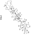
- FIG. 2 shows the construction of a first embodiment of a multi-beam light source unit according to the present invention.
- the semiconductor laser array 30 is press-fit or adhered on a support body 2.
- the support body 2 is connected to a back surface 3a of a rotary base 3 by screws. Holes in the support body 2 permit play with respect to the screws, so that it is possible to adjust the position of the semiconductor laser array 30 in upward, downward, rightward and leftward directions with respect to an optical axis A of the collimator lens 35.
- the collimator lens 35 (not visible in FIG. 2) is accommodated within a mirror pipe 6.
- This mirror pipe 6 is fitted into a fitting hole 3b of the rotary base 3 and is bonded to the rotary base 3 by matching the position in the direction of the optical axis A with respect to the semiconductor laser array 30.
- a sleeve shaft 3e of the rotary base 3 is provided concentrically to the fitting hole 3b.
- This sleeve shaft 3e fits into a fitting hole 10a of a base 10, and the rotary base 3 is rotatable about the sleeve shaft 3e.
- the center of rotation of the rotary base 3 matches or substantially matches the optical axis A of the collimator lens 35.
- the rotary base 3 is fixed to the base 10 by screws 11 after adjustment of the multi-beam light source unit.
- a substrate 7 including a driving circuit for the semiconductor laser array 30 is fixed on bosses 3d of the rotary base 3 by screws 8.
- the multi-beam light source unit is mounted on an optical housing 12 of the multi-beam scanner via positioning pins 12a and 12b which fit into corresponding positioning holes 10b and 10c of the base 10, so that the multi-beam light source unit is mounted with a spatial distance determined by a mounting surface 12c.
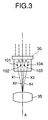
- FIG. 3 shows a relationship of the semiconductor laser array 30 and the collimator lens 35.
- FIGS. 4A and 4B respectively show positions of beam spots in a vertical direction (sub scanning direction or pixel density pitch direction) at imaging positions.
- the semiconductor laser array 30 has 4 light sources 101, 102, 103 and 104.
- the position of the support body 2 is adjusted in the upward, downward, rightward and leftward directions so that the optical axis A of the collimator lens 35 matches a center between the light sources 101 and 104 at both ends of the semiconductor laser array 30 among the 4 light sources 101 through 104 which are arranged at equal intervals, as shown in FIG. 3.
- a distance X1 from the light source 101 to the collimator lens 35, a distance X2 from the light source 102 to the collimator lens 35, a distance X3 from the light source 103 to the collimator lens 35, and a distance X4 from the light source 104 to the collimator lens 35 become substantially the same.
- a pitch p of the light sources 101 through 104 is extremely small and is on the order of several tens of ⁇ m. For this reason, all of the laser beams from the light source 101 through 104 pass a vicinity of the optical axis A, and a pixel density pitch P and a beam diameter D become approximately uniform at the imaging position for each of the laser beams, as shown in FIG. 4A.
- a rotation takes place substantially about the optical axis A, and the pixel density pitch P decreases to a pixel density pitch P' as shown in FIG. 4B.
- the beam position Since the rotation takes place in the vicinity of the center of the light sources, the beam position will not greatly deviate due to the rotation.
- the beam position is thus extremely stable, and is adjustable with a high accuracy. It is possible to maintain compatibility among independent multi-beam light source units by adjusting a rotary position of the multi-beam light source unit by an adjusting tool when adjusting the pixel density pitch P' by this rotation.
- the positioning of the rotary position of the multi-beam light source unit is achieved by the positioning holes 10b and 10c provided in the base 10, and the corresponding positioning pins 12a and 12b of the housing 12 which fit into these positioning holes 10b and 10c, as shown in FIG. 2.
- the base 10 is positioned by the optical housing 12 and the adjusting tool, so that the base 10 is arranged at the same position as the imaging position of the laser beams. Accordingly, even if it becomes necessary to replace the multi-beam light source unit, it becomes possible to mount a new multi-beam light source unit without adjusting the rotary position thereof.
- the position of the semiconductor laser array 30 is adjusted.
- FIG. 5 shows the construction of the second embodiment of the multi-beam light source unit.
- those parts which are the same as those corresponding parts in FIG. 2 are designated by the same reference numerals, and a description thereof will be omitted.
- the collimator lens 35 is bonded or press-fit within a mirror pipe 60.
- the mirror pipe 60 is bonded within the fitting hole 3b of the rotary base 3, by matching the position with respect to the semiconductor laser array 30 in the direction of the optical axis A.
- the mirror pipe 60 is fixed within the fitting hole 3b of the rotary base 3 by screws (not shown) or the like.
- the mirror pipe 60 which is fixed to the rotary base 3 fits into the fitting hole 10a of the base 10, and the mirror pipe 60 is rotatable about an outer diameter 60a of the mirror pipe 60.
- an outer diameter of a lens and an optical axis of the lens can be formed at a high precision with respect to each other, and eccentricity thereof can be suppressed.
- the outer diameter 60a of the mirror pipe 60 and an inner fitting part 60b of the mirror pipe 60 into which the collimator lens 35 fits can be formed by a common process, thereby guaranteeing coaxial accuracy of the outer diameter 60a and the inner fitting part 60b. Therefore, the center of the outer diameter 60a of the mirror pipe 60 and the optical axis A of the collimator lens 35 accurately match.
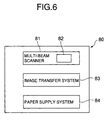
- FIG. 6 shows an embodiment of an image forming apparatus according to the present invention.
- the present invention is applied to any image forming apparatus which uses a multi-beam scanner, such as a laser printer, a digital copying machine, a facsimile machine, and a composite machine which has the functions of two or more of the laser printer, the copying machine and the facsimile machine.
- a multi-beam scanner such as a laser printer, a digital copying machine, a facsimile machine, and a composite machine which has the functions of two or more of the laser printer, the copying machine and the facsimile machine.
- An image forming apparatus 80 shown in FIG. 6 generally includes a multi-beam scanner 81 provided with a multi-beam light source unit 82, an image transfer system 83 which develops an image formed on the photoconductive drum within the multi-beam scanner 81 and transfers the developed image on a recording medium such as paper, and a paper supply system 84 which supplies the paper.
- the multi-beam scanner 81 has a construction shown in FIG. 1, for example. Further, the multi-beam light source unit 82 has a construction shown in FIG. 2 or 5, for example.
- the multi-beam light source unit 82 is constructed so that constituent elements thereof are provided within a single package.
- the image transfer system 83 and the paper supply system 84 may have known constructions employed by known image forming apparatuses.
Landscapes
- Physics & Mathematics (AREA)
- General Physics & Mathematics (AREA)
- Optics & Photonics (AREA)
- Engineering & Computer Science (AREA)
- Multimedia (AREA)
- Signal Processing (AREA)
- Mechanical Optical Scanning Systems (AREA)
- Facsimile Scanning Arrangements (AREA)
- Laser Beam Printer (AREA)
Applications Claiming Priority (4)
| Application Number | Priority Date | Filing Date | Title |
|---|---|---|---|
| JP22940998 | 1998-07-29 | ||
| JP22940998 | 1998-07-29 | ||
| JP10375098A JP2000105347A (ja) | 1998-07-29 | 1998-12-11 | マルチビ―ム光源装置、マルチビ―ム走査装置および画像形成装置 |
| JP37509898 | 1998-12-11 |
Publications (3)
| Publication Number | Publication Date |
|---|---|
| EP0977422A2 true EP0977422A2 (de) | 2000-02-02 |
| EP0977422A3 EP0977422A3 (de) | 2001-07-11 |
| EP0977422B1 EP0977422B1 (de) | 2003-09-17 |
Family
ID=26528779
Family Applications (1)
| Application Number | Title | Priority Date | Filing Date |
|---|---|---|---|
| EP99114251A Expired - Lifetime EP0977422B1 (de) | 1998-07-29 | 1999-07-28 | Mehrstrahllichtquelle, Mehrstrahlabtaster und Bilderzeugungsgerät |
Country Status (5)
| Country | Link |
|---|---|
| US (1) | US6320647B1 (de) |
| EP (1) | EP0977422B1 (de) |
| JP (1) | JP2000105347A (de) |
| DE (1) | DE69911332T2 (de) |
| ES (1) | ES2205654T3 (de) |
Cited By (2)
| Publication number | Priority date | Publication date | Assignee | Title |
|---|---|---|---|---|
| CN110568717A (zh) * | 2019-09-25 | 2019-12-13 | 天逸瑞狮(苏州)口腔医疗科技股份有限公司 | 一种影像扫描设备的光束调整装置 |
| CN112567294A (zh) * | 2018-08-16 | 2021-03-26 | 索尼公司 | 光源装置和投影型显示装置 |
Families Citing this family (13)
| Publication number | Priority date | Publication date | Assignee | Title |
|---|---|---|---|---|
| JP2001281578A (ja) * | 2000-03-30 | 2001-10-10 | Ricoh Co Ltd | マルチビーム走査装置及び画像形成装置 |
| JP2004126482A (ja) * | 2002-08-01 | 2004-04-22 | Ricoh Co Ltd | マルチビーム光源装置およびマルチビーム走査装置 |
| US7151556B2 (en) * | 2002-08-23 | 2006-12-19 | Samsung Electronics Co., Ltd. | Sub-scanning interval adjusting apparatus for multi-beam scanning unit |
| EP1439070B1 (de) * | 2003-01-20 | 2008-10-29 | Ricoh Company, Ltd. | Mehrstrahlabtastgerät und Bilderzeugungsgerät mit einem solchen Abtastgerät |
| JP2004246137A (ja) * | 2003-02-14 | 2004-09-02 | Pentax Corp | レーザ走査装置 |
| KR100579491B1 (ko) * | 2003-11-01 | 2006-05-15 | 삼성전자주식회사 | 멀티-빔 광원 유닛과, 이를 구비하는 레이저 스캐닝 유닛및 그조립방법 |
| KR100579505B1 (ko) * | 2003-11-05 | 2006-05-15 | 삼성전자주식회사 | 멀티-빔 광원 유닛 및 이를 구비하는 레이저 스캐닝 유닛 |
| JP4922694B2 (ja) * | 2006-08-09 | 2012-04-25 | 株式会社リコー | 光線変位算出方法、光走査装置、及び画像形成装置 |
| JP2009098542A (ja) * | 2007-10-19 | 2009-05-07 | Hoya Corp | マルチビーム走査装置 |
| US8542263B2 (en) * | 2010-03-15 | 2013-09-24 | Fuji Xerox Co., Ltd. | Mounting structure of a mounted component, light scanning device, and image forming apparatus |
| JP5449302B2 (ja) * | 2011-12-08 | 2014-03-19 | 京セラドキュメントソリューションズ株式会社 | 光走査装置、及びこれを用いた画像形成装置 |
| JP2016188966A (ja) * | 2015-03-30 | 2016-11-04 | 京セラドキュメントソリューションズ株式会社 | 光走査装置のビーム調整方法及び光走査装置 |
| JP6946983B2 (ja) | 2017-11-30 | 2021-10-13 | 株式会社リコー | 位置検出装置、画像読取装置、画像形成装置、プログラムおよび位置検出方法 |
Family Cites Families (18)
| Publication number | Priority date | Publication date | Assignee | Title |
|---|---|---|---|---|
| JPS5642248A (en) | 1979-09-14 | 1981-04-20 | Canon Inc | Light source device |
| US4393387A (en) * | 1979-09-14 | 1983-07-12 | Canon Kabushiki Kaisha | Beam recording apparatus effecting the recording by a plurality of beams |
| JPH0727988A (ja) * | 1993-07-08 | 1995-01-31 | Canon Inc | 光走査装置 |
| JPH08136841A (ja) * | 1994-11-08 | 1996-05-31 | Canon Inc | レ−ザユニット及び画像形成装置 |
| US5753907A (en) * | 1995-05-24 | 1998-05-19 | Ricoh Company, Ltd. | Multiple beam scanning apparatus |
| JPH0926550A (ja) | 1995-07-10 | 1997-01-28 | Ricoh Co Ltd | マルチビーム走査装置 |
| JPH0933834A (ja) * | 1995-07-21 | 1997-02-07 | Canon Inc | 2ビームレーザー走査光学系 |
| JP3545115B2 (ja) * | 1995-09-22 | 2004-07-21 | 大日本スクリーン製造株式会社 | 像面湾曲の補正方法および該方法に使用する光ビーム走査装置 |
| JPH09251137A (ja) * | 1996-03-15 | 1997-09-22 | Konica Corp | レーザ記録装置 |
| JPH1010447A (ja) * | 1996-06-24 | 1998-01-16 | Canon Inc | 光走査装置 |
| JPH1010448A (ja) * | 1996-06-24 | 1998-01-16 | Canon Inc | 光走査装置 |
| JPH10193680A (ja) * | 1997-01-10 | 1998-07-28 | Fujitsu Ltd | 光源装置とそれを用いた画像形成装置 |
| JPH10319338A (ja) | 1997-05-16 | 1998-12-04 | Canon Inc | レーザー光発生装置及び光源調整方法 |
| US5999345A (en) * | 1997-07-03 | 1999-12-07 | Ricoh Company, Ltd. | Multi-beam light source unit |
| JP3679560B2 (ja) * | 1997-08-22 | 2005-08-03 | キヤノン株式会社 | 走査光学系の調整方法 |
| JPH1158829A (ja) | 1997-08-26 | 1999-03-02 | Canon Inc | レーザー光源装置 |
| JPH1172729A (ja) | 1997-08-29 | 1999-03-16 | Canon Inc | マルチビーム走査装置 |
| JPH11202230A (ja) * | 1998-01-14 | 1999-07-30 | Fuji Xerox Co Ltd | 光走査装置 |
-
1998
- 1998-12-11 JP JP10375098A patent/JP2000105347A/ja active Pending
-
1999
- 1999-07-28 US US09/361,993 patent/US6320647B1/en not_active Expired - Fee Related
- 1999-07-28 EP EP99114251A patent/EP0977422B1/de not_active Expired - Lifetime
- 1999-07-28 DE DE69911332T patent/DE69911332T2/de not_active Expired - Lifetime
- 1999-07-28 ES ES99114251T patent/ES2205654T3/es not_active Expired - Lifetime
Cited By (2)
| Publication number | Priority date | Publication date | Assignee | Title |
|---|---|---|---|---|
| CN112567294A (zh) * | 2018-08-16 | 2021-03-26 | 索尼公司 | 光源装置和投影型显示装置 |
| CN110568717A (zh) * | 2019-09-25 | 2019-12-13 | 天逸瑞狮(苏州)口腔医疗科技股份有限公司 | 一种影像扫描设备的光束调整装置 |
Also Published As
| Publication number | Publication date |
|---|---|
| DE69911332T2 (de) | 2004-07-01 |
| EP0977422A3 (de) | 2001-07-11 |
| ES2205654T3 (es) | 2004-05-01 |
| US6320647B1 (en) | 2001-11-20 |
| JP2000105347A (ja) | 2000-04-11 |
| EP0977422B1 (de) | 2003-09-17 |
| DE69911332D1 (de) | 2003-10-23 |
Similar Documents
| Publication | Publication Date | Title |
|---|---|---|
| US7460145B2 (en) | Multi-beam pitch adjusting apparatus and image forming apparatus | |
| US6320647B1 (en) | Multi-beam light source unit, multi-beam scanner and image forming apparatus | |
| US8120830B2 (en) | Optical scanning apparatus | |
| US4816844A (en) | Superimposed image forming apparatus | |
| JP4027293B2 (ja) | 走査光学装置 | |
| JP4349483B2 (ja) | 光走査装置および画像形成装置 | |
| US6961077B2 (en) | Multibeam light source | |
| EP0773461B1 (de) | Verfahren und Vorrichtung zur Mehrstrahlabtastung | |
| JPH0933834A (ja) | 2ビームレーザー走査光学系 | |
| JP2000075227A (ja) | マルチビーム光源装置 | |
| CN100448682C (zh) | 预扫描组件,后扫描组件,激光扫描彩色成像装置,彩色激光打印机 | |
| JPH10133130A (ja) | 多色画像形成装置の光走査装置 | |
| US6144478A (en) | Flexible arm piezoelectric lens mover | |
| JP2005201941A (ja) | 走査光学装置 | |
| JPH0926550A (ja) | マルチビーム走査装置 | |
| JPH10319336A (ja) | マルチビーム光源装置およびこれを用いた光偏向走査装置 | |
| JP2006194973A (ja) | 光走査装置 | |
| JP3470040B2 (ja) | カラー画像形成装置 | |
| JP2002333588A (ja) | 光走査装置及び画像形成装置 | |
| JP2001042238A (ja) | マルチビーム走査装置 | |
| JP2001166242A (ja) | 光走査装置およびミラー面調節装置 | |
| US7042481B2 (en) | Laser exposing apparatus | |
| JP2003322821A (ja) | 光走査装置及びそれを備えた画像形成装置 | |
| JP2001264659A (ja) | 光走査装置及び光ビーム走査位置調整方法 | |
| JPH05289008A (ja) | 同期検出装置 |
Legal Events
| Date | Code | Title | Description |
|---|---|---|---|
| PUAI | Public reference made under article 153(3) epc to a published international application that has entered the european phase |
Free format text: ORIGINAL CODE: 0009012 |
|
| AK | Designated contracting states |
Kind code of ref document: A2 Designated state(s): DE ES FR GB IT NL |
|
| AX | Request for extension of the european patent |
Free format text: AL;LT;LV;MK;RO;SI |
|
| PUAL | Search report despatched |
Free format text: ORIGINAL CODE: 0009013 |
|
| AK | Designated contracting states |
Kind code of ref document: A3 Designated state(s): AT BE CH CY DE DK ES FI FR GB GR IE IT LI LU MC NL PT SE |
|
| AX | Request for extension of the european patent |
Free format text: AL;LT;LV;MK;RO;SI |
|
| RIC1 | Information provided on ipc code assigned before grant |
Free format text: 7H 04N 1/113 A, 7G 02B 26/12 B, 7H 04N 1/191 B |
|
| 17P | Request for examination filed |
Effective date: 20020102 |
|
| AKX | Designation fees paid |
Free format text: DE ES FR GB IT NL |
|
| 17Q | First examination report despatched |
Effective date: 20020328 |
|
| GRAH | Despatch of communication of intention to grant a patent |
Free format text: ORIGINAL CODE: EPIDOS IGRA |
|
| GRAS | Grant fee paid |
Free format text: ORIGINAL CODE: EPIDOSNIGR3 |
|
| GRAA | (expected) grant |
Free format text: ORIGINAL CODE: 0009210 |
|
| AK | Designated contracting states |
Kind code of ref document: B1 Designated state(s): DE ES FR GB IT NL |
|
| REG | Reference to a national code |
Ref country code: GB Ref legal event code: FG4D |
|
| REF | Corresponds to: |
Ref document number: 69911332 Country of ref document: DE Date of ref document: 20031023 Kind code of ref document: P |
|
| REG | Reference to a national code |
Ref country code: ES Ref legal event code: FG2A Ref document number: 2205654 Country of ref document: ES Kind code of ref document: T3 |
|
| ET | Fr: translation filed | ||
| PLBE | No opposition filed within time limit |
Free format text: ORIGINAL CODE: 0009261 |
|
| STAA | Information on the status of an ep patent application or granted ep patent |
Free format text: STATUS: NO OPPOSITION FILED WITHIN TIME LIMIT |
|
| 26N | No opposition filed |
Effective date: 20040618 |
|
| PGFP | Annual fee paid to national office [announced via postgrant information from national office to epo] |
Ref country code: FR Payment date: 20110729 Year of fee payment: 13 |
|
| PGFP | Annual fee paid to national office [announced via postgrant information from national office to epo] |
Ref country code: DE Payment date: 20110722 Year of fee payment: 13 Ref country code: ES Payment date: 20110719 Year of fee payment: 13 Ref country code: GB Payment date: 20110721 Year of fee payment: 13 |
|
| PGFP | Annual fee paid to national office [announced via postgrant information from national office to epo] |
Ref country code: NL Payment date: 20110726 Year of fee payment: 13 Ref country code: IT Payment date: 20110722 Year of fee payment: 13 |
|
| REG | Reference to a national code |
Ref country code: NL Ref legal event code: V1 Effective date: 20130201 |
|
| GBPC | Gb: european patent ceased through non-payment of renewal fee |
Effective date: 20120728 |
|
| REG | Reference to a national code |
Ref country code: FR Ref legal event code: ST Effective date: 20130329 |
|
| PG25 | Lapsed in a contracting state [announced via postgrant information from national office to epo] |
Ref country code: NL Free format text: LAPSE BECAUSE OF NON-PAYMENT OF DUE FEES Effective date: 20130201 Ref country code: DE Free format text: LAPSE BECAUSE OF NON-PAYMENT OF DUE FEES Effective date: 20130201 Ref country code: GB Free format text: LAPSE BECAUSE OF NON-PAYMENT OF DUE FEES Effective date: 20120728 Ref country code: FR Free format text: LAPSE BECAUSE OF NON-PAYMENT OF DUE FEES Effective date: 20120731 |
|
| REG | Reference to a national code |
Ref country code: DE Ref legal event code: R119 Ref document number: 69911332 Country of ref document: DE Effective date: 20130201 |
|
| PG25 | Lapsed in a contracting state [announced via postgrant information from national office to epo] |
Ref country code: IT Free format text: LAPSE BECAUSE OF NON-PAYMENT OF DUE FEES Effective date: 20120728 |
|
| REG | Reference to a national code |
Ref country code: ES Ref legal event code: FD2A Effective date: 20131021 |
|
| PG25 | Lapsed in a contracting state [announced via postgrant information from national office to epo] |
Ref country code: ES Free format text: LAPSE BECAUSE OF NON-PAYMENT OF DUE FEES Effective date: 20120729 |