EP0982753A2 - Anzeigetafel und Entladungs-Anzeigegerät - Google Patents
Anzeigetafel und Entladungs-Anzeigegerät Download PDFInfo
- Publication number
- EP0982753A2 EP0982753A2 EP99306501A EP99306501A EP0982753A2 EP 0982753 A2 EP0982753 A2 EP 0982753A2 EP 99306501 A EP99306501 A EP 99306501A EP 99306501 A EP99306501 A EP 99306501A EP 0982753 A2 EP0982753 A2 EP 0982753A2
- Authority
- EP
- European Patent Office
- Prior art keywords
- gas
- discharge
- mixed
- mixed ratio
- operating margin
- Prior art date
- Legal status (The legal status is an assumption and is not a legal conclusion. Google has not performed a legal analysis and makes no representation as to the accuracy of the status listed.)
- Withdrawn
Links
Images

Classifications
-
- H—ELECTRICITY
- H01—ELECTRIC ELEMENTS
- H01J—ELECTRIC DISCHARGE TUBES OR DISCHARGE LAMPS
- H01J11/00—Gas-filled discharge tubes with alternating current induction of the discharge, e.g. alternating current plasma display panels [AC-PDP]; Gas-filled discharge tubes without any main electrode inside the vessel; Gas-filled discharge tubes with at least one main electrode outside the vessel
- H01J11/10—AC-PDPs with at least one main electrode being out of contact with the plasma
- H01J11/12—AC-PDPs with at least one main electrode being out of contact with the plasma with main electrodes provided on both sides of the discharge space
-
- H—ELECTRICITY
- H01—ELECTRIC ELEMENTS
- H01J—ELECTRIC DISCHARGE TUBES OR DISCHARGE LAMPS
- H01J11/00—Gas-filled discharge tubes with alternating current induction of the discharge, e.g. alternating current plasma display panels [AC-PDP]; Gas-filled discharge tubes without any main electrode inside the vessel; Gas-filled discharge tubes with at least one main electrode outside the vessel
- H01J11/20—Constructional details
- H01J11/50—Filling, e.g. selection of gas mixture
Definitions
- the front glass substrate 1 is positioned opposed to the rear glass substrate 8 so that the surface of the protecting layer 7 comes into contact with the top face of the barrier ribs 11.
- the discharge spaces 13 are each enclosed by the protecting layer 7, barrier ribs 11 and dielectric layer 10.
- the wall surface of the barrier rib 11 and the top face of the dielectric layer 10 are coated with the phosphor 12.
- a region comprising a pair of an X electrode 2 and a Y electrode 3 constitutes a cell that is a pixel unit.
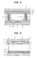
- Fig. 5 is a cross-sectional view of the PDP in Fig. 4 taken in an arrowed direction D1 and showing a single cell. Those parts already shown in Fig. 4 are indicated by like reference numerals.
- Fig. 6 is a cross-sectional view of the PDP in Fig. 4 taken in an arrowed direction D2 and also showing a single cell. Those parts that already appeared in Fig. 4 are denoted by like reference numerals. Although broken lines are used in Fig. 6 to indicate cell boundaries, cells are not actually segmented by walls as might be suggested by the lines.
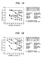
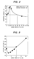
- the mixed ratio of the Xe gas component is specifically determined so that the sustain voltage is kept at an appropriate level.
Landscapes
- Physics & Mathematics (AREA)
- Engineering & Computer Science (AREA)
- Plasma & Fusion (AREA)
- Gas-Filled Discharge Tubes (AREA)
- Discharge Lamp (AREA)
- Devices For Indicating Variable Information By Combining Individual Elements (AREA)
Applications Claiming Priority (2)
| Application Number | Priority Date | Filing Date | Title |
|---|---|---|---|
| JP24023198 | 1998-08-26 | ||
| JP24023198A JP4011746B2 (ja) | 1998-08-26 | 1998-08-26 | プラズマディスプレイパネル |
Publications (2)
| Publication Number | Publication Date |
|---|---|
| EP0982753A2 true EP0982753A2 (de) | 2000-03-01 |
| EP0982753A3 EP0982753A3 (de) | 2000-04-19 |
Family
ID=17056410
Family Applications (1)
| Application Number | Title | Priority Date | Filing Date |
|---|---|---|---|
| EP99306501A Withdrawn EP0982753A3 (de) | 1998-08-26 | 1999-08-18 | Anzeigetafel und Entladungs-Anzeigegerät |
Country Status (4)
| Country | Link |
|---|---|
| US (1) | US6747410B1 (de) |
| EP (1) | EP0982753A3 (de) |
| JP (1) | JP4011746B2 (de) |
| KR (1) | KR100349274B1 (de) |
Families Citing this family (5)
| Publication number | Priority date | Publication date | Assignee | Title |
|---|---|---|---|---|
| JP2001228823A (ja) * | 1999-12-07 | 2001-08-24 | Pioneer Electronic Corp | プラズマディスプレイ装置 |
| KR20020047882A (ko) * | 2000-12-14 | 2002-06-22 | 엘지전자 주식회사 | 플라즈마 표시 장치의 혼합 방전가스 |
| JP4271902B2 (ja) * | 2002-05-27 | 2009-06-03 | 株式会社日立製作所 | プラズマディスプレイパネル及びそれを用いた画像表示装置 |
| KR100627265B1 (ko) * | 2003-11-29 | 2006-09-25 | 삼성에스디아이 주식회사 | 플라즈마 디스플레이 패널 |
| JP4650824B2 (ja) * | 2004-09-10 | 2011-03-16 | パナソニック株式会社 | プラズマディスプレイパネル |
Citations (2)
| Publication number | Priority date | Publication date | Assignee | Title |
|---|---|---|---|---|
| US5661500A (en) * | 1992-01-28 | 1997-08-26 | Fujitsu Limited | Full color surface discharge type plasma display device |
| US5757131A (en) * | 1995-08-11 | 1998-05-26 | Nec Corporation | Color plasma display panel and fabricating method |
Family Cites Families (16)
| Publication number | Priority date | Publication date | Assignee | Title |
|---|---|---|---|---|
| US3903445A (en) * | 1971-10-04 | 1975-09-02 | Owens Illinois Inc | Display/memory panel having increased memory margin |
| JPS63205031A (ja) * | 1987-02-19 | 1988-08-24 | Fujitsu Ltd | ガス放電パネル |
| JPH0624116B2 (ja) | 1987-10-28 | 1994-03-30 | 三菱電機株式会社 | 熱陰極形低圧希ガス放電蛍光ランプ |
| JP2671575B2 (ja) * | 1989-11-22 | 1997-10-29 | 日本電気株式会社 | ガス放電表示素子の駆動方法 |
| JP2616538B2 (ja) | 1993-06-01 | 1997-06-04 | 日本電気株式会社 | ガス放電型表示装置 |
| JPH0721928A (ja) | 1993-06-30 | 1995-01-24 | Matsushita Electron Corp | 気体放電型表示装置 |
| JPH07134948A (ja) * | 1993-11-10 | 1995-05-23 | Oki Electric Ind Co Ltd | 気体放電発光装置 |
| JPH08185802A (ja) * | 1994-12-28 | 1996-07-16 | Noritake Co Ltd | 放電表示装置 |
| JP3339554B2 (ja) | 1995-12-15 | 2002-10-28 | 松下電器産業株式会社 | プラズマディスプレイパネル及びその製造方法 |
| JP2930007B2 (ja) * | 1996-05-30 | 1999-08-03 | 日本電気株式会社 | ガス放電型表示装置 |
| JP3106992B2 (ja) * | 1997-02-20 | 2000-11-06 | 日本電気株式会社 | Ac面放電型プラズマディスプレイパネル |
| KR100226834B1 (ko) * | 1997-06-27 | 1999-10-15 | 구자홍 | 칼라 플라즈마 디스플레이 패널의 상부전극 구조 |
| KR100290839B1 (ko) * | 1997-06-27 | 2001-10-23 | 구자홍 | 3성분의 혼합가스가 충전된 칼라 피디피 |
| US6194831B1 (en) * | 1997-09-12 | 2001-02-27 | Lg Electronics Inc. | Gas discharge display |
| US6232717B1 (en) * | 1997-11-17 | 2001-05-15 | Nec Corporation | AC type color plasma display panel |
| JP2000188062A (ja) * | 1998-12-24 | 2000-07-04 | Hitachi Ltd | プラズマディスプレイ装置 |
-
1998
- 1998-08-26 JP JP24023198A patent/JP4011746B2/ja not_active Expired - Fee Related
-
1999
- 1999-08-18 EP EP99306501A patent/EP0982753A3/de not_active Withdrawn
- 1999-08-24 US US09/379,471 patent/US6747410B1/en not_active Expired - Fee Related
- 1999-08-25 KR KR1019990035316A patent/KR100349274B1/ko not_active Expired - Fee Related
Patent Citations (2)
| Publication number | Priority date | Publication date | Assignee | Title |
|---|---|---|---|---|
| US5661500A (en) * | 1992-01-28 | 1997-08-26 | Fujitsu Limited | Full color surface discharge type plasma display device |
| US5757131A (en) * | 1995-08-11 | 1998-05-26 | Nec Corporation | Color plasma display panel and fabricating method |
Also Published As
| Publication number | Publication date |
|---|---|
| EP0982753A3 (de) | 2000-04-19 |
| JP4011746B2 (ja) | 2007-11-21 |
| KR20000017502A (ko) | 2000-03-25 |
| JP2000067758A (ja) | 2000-03-03 |
| US6747410B1 (en) | 2004-06-08 |
| KR100349274B1 (ko) | 2002-08-21 |
Similar Documents
| Publication | Publication Date | Title |
|---|---|---|
| KR100433213B1 (ko) | 플라즈마 디스플레이 패널의 구동방법 및 장치 | |
| US8035579B2 (en) | Plasma display panel driving method, plasma display panel gray displaying method, and plasma display device | |
| JP3429438B2 (ja) | Ac型pdpの駆動方法 | |
| US20020050794A1 (en) | Method for driving AC plama display | |
| JPH09274465A (ja) | Ac型pdpの駆動方法及び表示装置 | |
| KR20040000327A (ko) | 플라즈마표시패널 및 그 구동방법 | |
| JP2005025224A (ja) | プラズマディスプレーパネルの駆動方法及びプラズマディスプレーパネルの駆動装置 | |
| JP2003346660A (ja) | プラズマディスプレイパネル及びそれを用いた画像表示装置 | |
| KR19990074718A (ko) | 교류형 플라즈마 디스플레이 패널 및 구동 방법 | |
| JP3328932B2 (ja) | プラズマディスプレイパネルの駆動方法 | |
| JP2005122102A (ja) | プラズマディスプレイパネルとその駆動方法 | |
| US6747410B1 (en) | Display panel and discharge type display apparatus having mixture of three gases | |
| US7576710B2 (en) | Plasma display panel and driving method thereof | |
| US6995735B2 (en) | Drive method of AC type plasma display panel | |
| EP1868177A2 (de) | Plasmaanzeigevorrichtung und Verfahren zu ihrer Ansteuerung | |
| CN1224211A (zh) | 驱动ac型等离子显示板的方法 | |
| US7486260B2 (en) | Plasma display panel having a driving apparatus and method for displaying pictures | |
| KR20030090370A (ko) | 3전극 면방전형 교류 플라즈마 디스플레이 패널 | |
| EP1538589A2 (de) | Verfahren zur Steuerung einer Plasmaanzeigevorrichtung | |
| KR100577162B1 (ko) | 플라즈마 표시소자 및 그 구동 방법 | |
| WO2009125910A1 (en) | Plasma display device | |
| KR100647616B1 (ko) | 플라즈마 디스플레이 패널의 구동방법 | |
| KR100472370B1 (ko) | 플라즈마 디스플레이 패널 및 그 구동방법 | |
| KR100515339B1 (ko) | 플라즈마 표시 패널 및 그의 구동방법 | |
| KR100637176B1 (ko) | 플라즈마 디스플레이 패널 |
Legal Events
| Date | Code | Title | Description |
|---|---|---|---|
| PUAI | Public reference made under article 153(3) epc to a published international application that has entered the european phase |
Free format text: ORIGINAL CODE: 0009012 |
|
| 17P | Request for examination filed |
Effective date: 19990907 |
|
| AK | Designated contracting states |
Kind code of ref document: A2 Designated state(s): DE FR IT NL |
|
| AX | Request for extension of the european patent |
Free format text: AL;LT;LV;MK;RO;SI |
|
| PUAL | Search report despatched |
Free format text: ORIGINAL CODE: 0009013 |
|
| AK | Designated contracting states |
Kind code of ref document: A3 Designated state(s): AT BE CH CY DE DK ES FI FR GB GR IE IT LI LU MC NL PT SE |
|
| AX | Request for extension of the european patent |
Free format text: AL;LT;LV;MK;RO;SI |
|
| AKX | Designation fees paid |
Free format text: DE FR IT NL |
|
| 17Q | First examination report despatched |
Effective date: 20030115 |
|
| RAP1 | Party data changed (applicant data changed or rights of an application transferred) |
Owner name: HITACHI, LTD. |
|
| APBN | Date of receipt of notice of appeal recorded |
Free format text: ORIGINAL CODE: EPIDOSNNOA2E |
|
| APBR | Date of receipt of statement of grounds of appeal recorded |
Free format text: ORIGINAL CODE: EPIDOSNNOA3E |
|
| APBV | Interlocutory revision of appeal recorded |
Free format text: ORIGINAL CODE: EPIDOSNIRAPE |
|
| 17Q | First examination report despatched |
Effective date: 20030115 |
|
| STAA | Information on the status of an ep patent application or granted ep patent |
Free format text: STATUS: THE APPLICATION HAS BEEN WITHDRAWN |
|
| 18W | Application withdrawn |
Effective date: 20080904 |