EP0982934A2 - Dispositif et méthode de correction de distorsion de balayage pour tubes à rayons cathodiques - Google Patents
Dispositif et méthode de correction de distorsion de balayage pour tubes à rayons cathodiques Download PDFInfo
- Publication number
- EP0982934A2 EP0982934A2 EP99402126A EP99402126A EP0982934A2 EP 0982934 A2 EP0982934 A2 EP 0982934A2 EP 99402126 A EP99402126 A EP 99402126A EP 99402126 A EP99402126 A EP 99402126A EP 0982934 A2 EP0982934 A2 EP 0982934A2
- Authority
- EP
- European Patent Office
- Prior art keywords
- image
- data
- correction data
- correcting
- display
- Prior art date
- Legal status (The legal status is an assumption and is not a legal conclusion. Google has not performed a legal analysis and makes no representation as to the accuracy of the status listed.)
- Withdrawn
Links
Images






Classifications
-
- H—ELECTRICITY
- H04—ELECTRIC COMMUNICATION TECHNIQUE
- H04N—PICTORIAL COMMUNICATION, e.g. TELEVISION
- H04N3/00—Scanning details of television systems; Combination thereof with generation of supply voltages
- H04N3/10—Scanning details of television systems; Combination thereof with generation of supply voltages by means not exclusively optical-mechanical
- H04N3/16—Scanning details of television systems; Combination thereof with generation of supply voltages by means not exclusively optical-mechanical by deflecting electron beam in cathode-ray tube, e.g. scanning corrections
- H04N3/22—Circuits for controlling dimensions, shape or centering of picture on screen
- H04N3/23—Distortion correction, e.g. for pincushion distortion correction, S-correction
-
- H—ELECTRICITY
- H04—ELECTRIC COMMUNICATION TECHNIQUE
- H04N—PICTORIAL COMMUNICATION, e.g. TELEVISION
- H04N3/00—Scanning details of television systems; Combination thereof with generation of supply voltages
- H04N3/10—Scanning details of television systems; Combination thereof with generation of supply voltages by means not exclusively optical-mechanical
- H04N3/16—Scanning details of television systems; Combination thereof with generation of supply voltages by means not exclusively optical-mechanical by deflecting electron beam in cathode-ray tube, e.g. scanning corrections
- H04N3/22—Circuits for controlling dimensions, shape or centering of picture on screen
- H04N3/23—Distortion correction, e.g. for pincushion distortion correction, S-correction
- H04N3/233—Distortion correction, e.g. for pincushion distortion correction, S-correction using active elements
- H04N3/2335—Distortion correction, e.g. for pincushion distortion correction, S-correction using active elements with calculating means
Definitions
- the present invention relates to an image display correcting system and image display correcting apparatus and method for correcting a display state such as distortion of a displayed image, and image display apparatus and method for displaying the corrected image.
- a CRT cathode ray tube
- an electron beam is emitted from an electron gun and the electron beam is deflected by a magnetic field or an electric field for deflection applied from the outside, thereby displaying an image.
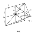
- Fig. 1 is a diagram showing a display screen of an image display apparatus using the CRT.
- an electron beam emitted from an electron gun is deflected both in the vertical and in the horizontal directions by a deflector using a deflecting coil and a scanned image called a raster is displayed on a display surface S (screen).
- the electron beam is deflected by scan signals having sawtooth waveforms. Denote the deflection center point of the electron beam by O, and the center point of the screen by Os.
- the distance 1 from the deflection center point O to a scan position of the electron beam on the display surface S can be given by r ⁇ tan ⁇ in which r is the distance from the deflection center point O to the display face S (distance from the deflection center point O to the screen center point Os) and ⁇ , is the deflection angle of the electron beam.
- Figs. 2A and 2B and Figs. 3A and 3B are diagrams for describing an image displayed on the CRT more specifically. Since the screen of the CRT has generally a rectangular shape, the emission length of the electron beam reaching each of the four corners of the screen of the CRT is the longest. Consequently, an image displayed on the screen usually looks distorted in a bobbin shape.
- the distortion of the image (hereinafter, called an "image distortion") can be expressed as a difference between an image inputted as an image signal (image to be displayed) and an image actually displayed on the screen of the CRT.
- Fig. 2A shows an image to be displayed and Fig. 2B illustrates a distorted image actually displayed on the screen (part shown by solid lines). In Fig. 2B, the part shown by broken lines denotes an image to be displayed.
- FIG. 3B shows an image accompanied by misconvergence which is actually displayed on the screen.
- Figs. 3A and 3B illustrate a case of the misconvergence when a cross hatch signal of white is displayed on the CRT.
- parts shown by reference numerals 100R, 100G, and 100B represent images of the colors of R, G, and B, respectively.
- a distortion of the electron beam such as image distortion and misconvergence influenced by the magnetic field is, although not much, influenced by earth magnetism and arrangement of components in the apparatus.
- the occurrence of the image distortion is conventionally minimized by optimizing the deflecting magnetic field generated by the deflecting yoke.
- the image distortion cannot be corrected with sufficient performance only by optimizing the deflecting magnetic field generated by the deflecting yoke.
- There are several methods of correcting the image distortion of an amount which has not been corrected by the deflecting magnetic field: one is to modulate a deflecting current passed to the deflecting yoke, and another is to modulate a signal supplied to the cathode of the electron gun, and the like are employed.
- the method of modulating the deflecting current requires an additional circuit for the modulation and this causes a problem of cost increase.
- a cheap circuit may be used in order to reduce the cost, there is another problem that it is difficult to perform accurate correction with a cheap circuit.
- the method of modulating the signal supplied to the cathode of the electron gun the image distortion in the same scan line, that is, in the lateral direction can be corrected, however, it is difficult to correct the image distortion in the vertical direction.
- the electron beams of the three colors is designed to converge to the same spot with respect to the whole screen on the basis of a distribution of deflecting magnetic fields generated by the deflecting yoke.
- a method adopted in the related art in order to correct the misconvergence of an amount which has not been corrected in the above-mentioned manner is to converge the electron beams accurately by adding a subyoke for correction independent of the originally used deflecting yoke and to move the electron beams for the respective colors color by color.
- This method requires a circuit for driving the subyoke as well as the subyoke itself thus resulting in the increase in resulting in the manufacturing cost.
- the method of correcting the image distortion and the misconvergence by optimizing the deflecting magnetic field has been generally used in the related art. Since it is necessary to repeatedly spread the image to the whole screen in each of the horizontal and vertical directions in order to adjust the correction by the deflecting magnetic field, there are problems of the low efficiency of the work and the variation according to the adjusting persons. Therefore it is not always possible to perform optimum adjustment of the image distortion. Additional components such as a complicated deflecting coil and an adjusting mechanism make the cost of the apparatus even higher.
- the correction amount is not so large. Therefore it is necessary to suppress variations in the assembly of the CRT and the deflecting yoke in order to suppress the image distortion and the misconvergence which are caused by variations in manufacturing of the CRT and the deflecting yoke to a certain degree. Since the image distortion and the misconvergence are also caused by the manufacturing variations of the CRT and the deflecting yoke in the image display apparatus of the related art, the CRT and the deflecting yoke have to be assembled with high accuracy, thereby incurring the high manufacturing cost.
- the invention has been achieved in consideration of the problems.
- the object is to provide an image display correcting system, image display correcting apparatus and method, and image display apparatus and method capable of displaying a high-quality image by correcting a defective display state, such as an image distortion, at a low cost.
- An image display correcting apparatus comprises: a correction data memory for storing correction data for correcting a display state of an image, obtained on the basis of an image displayed on a screen; and calculating means for performing an operation of correcting inputted image data on the basis of the correction data stored in the correction data memory so that an image is properly displayed and outputting the corrected image data as image data for display.
- An image display correcting method comprises: a step of storing correction data for correcting a display state of an image, obtained based on an image displayed on a screen; and a step of executing an operation of correcting inputted image data on the basis of the correction data stored in the storing step so that the image is properly displayed and outputting corrected image data as image data for display.
- An image display apparatus comprises: a correction data memory for storing correction data for correcting a display state of an image, obtained based on an image displayed on a screen; calculating means for executing an operation of correcting inputted image data on the basis of the correction data stored in the correction data memory so that an image is properly displayed and outputting the corrected image data as image data for display; and image display means for displaying an image on the basis of the image data for display outputted from the calculating means.
- An image display method comprises: a step of storing correction data for correcting a display state of an image, obtained based on an image displayed on a screen; a step of executing an operation of correcting inputted image data on the basis of the correction data stored in the storing step so that an image is properly displayed and outputting the corrected image data as image data for display; and a step of displaying an image on the basis of the image data for display outputted in the calculating step.
- An image display correcting system comprises an image display apparatus for displaying an image and a correction data forming apparatus for forming correction data for correcting an image displayed on the image display apparatus, wherein the correction data forming apparatus includes: an image pickup device for obtaining an image displayed on a screen of the image display apparatus; and an image distortion data calculating unit for forming correction data to correct a display state of an image, on the basis of the image obtained by the image pickup apparatus, and the image display apparatus includes: a correction data memory for storing correction data formed by the correction data forming apparatus; calculating means for executing an operation of correcting inputted image data on the basis of the correction data stored in the correction data memory so that an image is properly displayed and outputting the corrected image data as image data for display, and image display means for displaying an image on the basis of the image data for display outputted from the calculating means.
- a correcting operation is performed on inputted image data on the basis of correction data for correcting a display state of an image, obtained based on an image displayed on a screen so that an image is properly displayed, and the corrected image data is outputted as image data for display.
- a correcting operation is performed on inputted image data on the basis of correction data for correcting a display state of an image, obtained based on an image displayed on a screen so that an image is properly displayed and, the corrected image data is outputted as image data for display.
- An image is displayed on the basis of the outputted image data for display.
- an image displayed on the screen of the image display apparatus is obtained by the correction data forming apparatus and correction data for correcting a display state of the image is formed on the basis of the obtained image.
- a correcting operation is performed on inputted image data on the basis of the correction data formed by the correction data forming apparatus so that an image is properly displayed, and the corrected image data is outputted as image data for display. Then an image is displayed on the basis of the outputted image data for display.
- Fig. 1 is a diagram for explaining a display screen of an image display apparatus using a CRT.
- Fig. 2A is a diagram showing an image to be displayed on the CRT.
- Fig. 2B is a diagram showing an image accompanied by distortion displayed on the CRT.
- Fig. 3A is a diagram showing an image to be displayed on the CRT.
- Fig. 3B is a diagram showing an image accompanied by misconvergence displayed on the CRT.
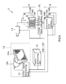
- Fig. 4 is a diagram showing a schematic construction of an image display correcting system according to the invention.
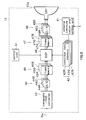
- Fig. 5 is a block diagram specifically showing an image display apparatus according to the invention.
- Fig. 6 is a diagram showing a screen region on a frame memory illustrated in Fig. 4.
- Fig. 7 is a diagram showing a deviation of a display position of a pixel due to image distortion or the like.
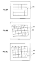
- Fig. 8A is a diagram showing an image on a frame memory at the front stage when a correcting operation is not performed.
- Fig. 8B is a diagram showing an image on a frame memory at the post stage when the correcting operation is not performed.
- Fig. 8C is a diagram showing an image on the CRT when the correcting operation is not performed.
- Fig. 9A is a diagram showing an image on the frame memory at the front stage when the correcting operation is performed.
- Fig. 9B is a diagram showing an image on the frame memory at the post stage when the correcting operation is performed.
- Fig. 9C is a diagram showing an image on the CRT when the correcting operation is performed.
- Fig. 10 is a diagram for explaining a first method of the correcting process in the image display apparatus.
- Fig. 11 is a diagram for explaining a second method of the correcting process in the image display apparatus.
- Fig. 12 is a diagram for explaining a third method in the correcting process in the image display apparatus.
- Fig. 13 is a diagram for explaining a method of obtaining a movement amount of a pixel in a divided region by interpolation.
- Fig. 14 is a diagram for explaining a method of obtaining a movement amount of a pixel in a divided region by extrapolation.
- Fig. 15 is a flowchart showing the third method of the correcting process in the image display apparatus.
- Fig. 16 is a block diagram specifically showing an image display apparatus according to another form of execution of the invention.
- Fig. 4 is a diagram showing a schematic construction of an image display correcting system according to the invention.
- the image display correcting system comprises: an image display apparatus 10 for displaying an image; and a correction data forming apparatus 1 for forming correction data used to correct an image displayed on the image display apparatus 10.
- the correction data forming apparatus 1 and the image display apparatus 10 are under the control of a control apparatus (not shown).
- the control apparatus takes the form of, for example, a microcomputer.
- the correction data formed by the correction data forming apparatus 1 is obtained by measuring an image distortion amount, a misconvergence amount, or the like of an image displayed on the image display apparatus 10.
- the correction data formed by the correction data forming apparatus 1 is automatically written into the image display apparatus 10 side.
- a defective display state such as image distortion or misconvergence is corrected on the basis of the correction data.
- the image display apparatus 10 is an apparatus subject to the correction of the display state of an image such as distortion.
- the image display apparatus 10 comprises: a CRT 10a in which a color image according to image signals supplied can be displayed on the screen; a deflector 10b for deflecting electron beams for scanning generated by the CRT 10a; and a video signal processing unit 11 for performing various signal processes on the inputted color image signal and supplying the resultant signal to the CRT 10a.
- the CRT 10a has, although not shown, an electron gun for generating an electron beam and the like.
- the deflector 10b has a deflecting coil and the like.
- the CRT 10a an electron beam emitted from the electron gun is deflected both in the vertical and in the horizontal directions by the deflector 10b to display a scan image called raster on the display face (screen).
- the detailed construction of the video signal processing unit 11 will be described hereinlater with reference to Fig. 5.
- the CRT 10a corresponds to "image display means" in an example of the invention.
- the correction data forming apparatus 1 comprises: a raster generating unit 12 for supplying a raster signal (image signal) including a reference signal, a horizontal synchronization signal HD, and a vertical synchronization signal VD to create a predetermined raster image on the image display apparatus 10; an image pickup apparatus 13 including, for example, an image pickup device such as CCD (Charge Coupled Device), for obtaining the image displayed on the CRT 10a of the image display apparatus 10 and outputting the image data; a frame memory 14 for storing the image data outputted from the image pickup apparatus 13 on a frame unit basis; an image distortion data calculating unit 15 for forming correction data to correct image distortion or the like on the basis of the image data stored in the frame memory 14; and a correction data memory 16 for storing the correction data created by the image distortion data calculating unit 15.
- a raster generating unit 12 for supplying a raster signal (image signal) including a reference signal, a horizontal synchronization signal HD, and a vertical synchronization signal V
- the frame memory 14 is a dual type memory to/from which data can be written/read and has a frame memory 14R for red, a frame memory 14G for green, and a frame memory 14B for blue.
- the correction data memory 16 has a correction data memory 16R for red, a correction data memory 16G for green, and a correction data memory 16B for blue.
- the raster generating unit 12 supplies reference image signals serving as a reference for correction which include signals for R, G, and B colors.
- reference image signal an image as a reference for correction is displayed on the screen of the CRT 10a of the image display apparatus 10.
- a raster image as a reference a dot pattern or a cross hatch pattern can be used. It is preferable that the reference image signal be also supplied to the image pickup apparatus 13 and the image distortion data calculating unit 15.
- the image pickup apparatus 13 obtains an image displayed on the screen of the CRT 10a in each of the R, G, and B colors and outputs the obtained image as image data color by color.
- the image data of R, G, and B outputted from the image pickup apparatus 13 is stored into the frame memories 14R for R, the frame memory 14G for G, and the frame memory 14B for B, respectively.
- storing means of other specifications such as a memory to which image data can be stored at least on a field unit basis may be used.
- the image distortion data calculating unit 15 determines the address (coordinates) position on the frame memory 14 corresponding to a picture plane having no distortion, to which the position of each pixel in a distorted image displayed on the screen of the CRT 10a corresponds, obtains correction data from data related to both of the address information, and stores the obtained correction data color by color into the correction data memory 16.
- the image distortion data calculating unit 15 takes the form of, for example, a microcomputer.
- the correction data stored in the correction data memory 16 is supplied to the video signal processing unit 11 in the image display apparatus 10.
- the correction data obtained by the image distortion data calculating unit 15 is data regarding a movement amount from a proper display position of each pixel in two-dimensional digitized image data showing an image displayed on the screen of the CRT 10a.
- the frame memory 14 may be omitted from the system configuration when a clock for specifying a timing at which image data in the image pickup apparatus 13 is outputted and a clock supplied to the image distortion data calculating unit 15 are synchronized.
- a clock for specifying a timing at which image data in the image pickup apparatus 13 is outputted and a clock supplied to the image distortion data calculating unit 15 are synchronized.
- the two clocks can be made synchronous.
- Fig. 5 is a block diagram specifically showing the image display apparatus 10 according to the invention.
- the diagram shows an example of a circuit for receiving an analog composite signal in the NTSC (National Television System Committee) system as an input signal D IN and displaying a motion image according to the signal.
- NTSC National Television System Committee
- the video signal processing unit 11 comprises: a correction data memory 42 (42R, 42G, 42B) for storing the correction data of each color formed by the correction data forming apparatus 1; an external communication and writing unit 41 for communicating with the correction data forming apparatus 1 as an external apparatus and writing the correction data formed by the correction data forming apparatus 1 into the correction data memory 42; a composite/RGB converter 43 for converting the analog composite signal inputted as an input signal D IN into a signal of R, G, or B; an analog/digital signal (hereinafter, referred to as "A/D") converter 44 (44R, 44G, 44B) for converting an analog signal for each color outputted from the composite/RGB converter 43 into a digital signal and outputting the digital signal; and a frame memory 45 (45R, 45G, 45B) for storing the digital signal of each color outputted from the A/D converter 44 on a frame unit basis.
- A/D analog/digital signal
- the video signal processing unit 11 further comprises a DSP (Digital Signal Processor) circuit 46 for performing various calculating processes on image data of each color stored in the frame memory 45 and outputting the calculated data color by color; a frame memory 47 (47R, 47G, 47B) for storing the calculated image data outputted from the DSP circuit 46 color by color on the frame unit basis; a digital/analog signal (hereinafter, referred to as "D/A") converter 48 (48R, 48G, 48B) for converting the image data stored in the frame memory 47 into an analog signal and outputting the analog signal to the CRT 10a; and a control unit 51 for instructing the calculating method to the DSP circuit 46.
- the frame memories 44 and 47 are dual type memories to/from which data can be written/read.
- the DSP circuit 46 corresponds to "calculating means" in an example of the invention.
- the DSP circuit 46 takes the form of, for example, a general one-chip LSI.
- the DSP circuit 46 performs the calculating process to correct the image distortion or misconvergence on the image data of each color stored in the frame memory 45 by using the correction data stored in the correction data memory 42 in accordance with an instruction of the control unit 51.
- the calculating process for correcting the image distortion or misconvergence will be described in detail hereinlater with reference to the drawings.
- the landing of the electron beam is adjusted to a certain extent so as to obtain desired accuracy.
- the screen size, display position, and the like are adjusted in advance so as to display an image of a predetermined size.
- the reference image signals for correction including signals of R, G, and B colors are supplied from the raster generating unit 12.
- the image display apparatus 10 displays a color image on the screen of the CRT 10a in accordance with the reference image signals supplied from the raster generating unit 12.
- the image displayed according to the reference image signal is, for example, a dot pattern or a grid pattern.
- the raster image as a reference for correction in the R, G, and B colors displayed on the screen of the CRT 10a is obtained by the image pickup apparatus 13 and the obtained image data is stored into the frame memory 14 on the frame unit basis.
- the image data stored in the frame memory 14 is supplied to the image distortion data calculating unit 15.
- the image distortion calculating unit 15 determines the address position on the frame memory 14 corresponding to the image having no distortion, to which the position of each pixel in a distorted image on the screen of the CRT 10a corresponds, forms the correction data from the data related to both of the address information, and stores the correction data into the correction data memory 16.
- the correction data stored in the correction data memory 16 on the correction data forming apparatus 1 side is transmitted to the image display apparatus 10.
- the correction data transmitted from the correction data forming apparatus 1 side is written into the correction data memory 42 by the external communication and writing unit 41 (Fig. 5).
- a defective display state such as image distortion or misconvergence is corrected on the basis of the correction data and the corrected image is displayed.
- a screen region on the frame memory 14 on the correction data forming apparatus 1 side is shown.
- a region 30 is a screen region on the frame memory 14.
- a region 31 is a screen region on the CRT 10a for an image obtained by the image pickup apparatus 13.
- the region 31 corresponds to a region of an effective screen on which the image is actually displayed on the screen of the CRT 10a.
- the size of image information which is supplied is larger than that of the screen on which the image is actually displayed.
- the difference between the actually displayed image and the original image corresponds to a region called an over-scan region.
- the image obtained by the image pickup apparatus 13 does not include the information of the over-scan region as a matter of course.
- the image out of the effective screen cannot be therefore detected.
- an image of the over-scan region is displayed on the screen due to an influence of the earth magnetism or the like.
- the correction data it is consequently desirable that the data in the over-scan region be obtained by estimating it by extrapolating information on the effective screen as well as the data in the region of the effective screen of the CRT 10a.
- the screen region on the frame memory 14 is set larger than the region of the effective screen of the CRT 10a in consideration of the over-scan region.
- the coordinates Ms are shown as an representative of coordinates MR, MG, and MB of pixels of the respective colors R, G, and B.
- the coordinates MR, MG, and MB are positioned on the same pixel.
- the pixel on the coordinates MR (n, m) is displayed in, for example, the position of the point Ar referred to with the mark of " ⁇ " in Fig. 7 on the frame memory 14 due to image distortion or the like on the image display apparatus 10.
- the pixel on the coordinates MG (n, m) is displayed, for example, in the position of the point Ag referred to with the mark of " ⁇ " in Fig. 7 on the frame memory 14 due to image distortion or the like on the image display apparatus 10.
- the pixel on the coordinates M B (n, m) is displayed, for example, in the position of the point Ab referred to with the mark of "o" in Fig. 7 on the frame memory 14 due to image distortion or the like on the image display apparatus 10.
- the image distortion data calculating unit 15 detects address information of each pixel position with respect to the whole raster image of each color deviated by, for example, image distortion or the like on the image display apparatus 10, calculates the correction data of each color from the address information of each color, and stores the calculated correction data of each color into the correction data memory 16.
- the image data correcting operation for correcting a defective display state such as image distortion, which is to be performed in the image display apparatus 10, will now be described.
- the correcting operation is performed for each of the colors R, G, and B.
- the calculating method is substantially the same with respect to the three colors though only the correcting data used for calculation is different.
- the correcting operation for the color R will be described hereinbelow as a representative and the description on the colors G and B is omitted here in otherwise described.
- Figs. 8A to 8C and Figs. 9A to 9C show the states where an input image is deformed in the image display apparatus 10.
- a grid image is inputted as an example of an input image.
- Figs. 8A and 9A illustrate images on the frame memory 45.
- Figs. 8B and 9B show images on the frame memory 47.
- Figs. 8C and 9C show images actually displayed on the screen of the CRT 10a.
- FIGs. 8A to 8C a state of deformation in an input image when the correcting operation using the correction data is not performed in the image display apparatus 10 will be described.
- an image 60 (Fig. 8A) on the frame memory 45 and an image 61 (Fig. 8B) on the frame memory 47 have the same shape as that of the input image.
- the image is distorted due to the characteristics of the CRT 10a and, for example, a deformed image 62 shown in Fig. 8C is displayed on the screen of the CRT 10a.
- the image shown by broken lines in Fig. 8C is the image 61 on the frame memory 47 which corresponds to an image to be displayed.
- the phenomenon that the same deformation occurs in the images of the colors R, G, and B in the process of displaying the image on the CRT 10a is the image distortion.
- performing deformation in the direction opposite to the characteristics of the CRT 10a at the stage before the image signal is supplied to the CRT 10a is sufficient.
- Figs. 9A, 9B, and 9C show a change in the input image when the correcting operation is performed in the image display apparatus 10.
- the image 60 (Fig. 9A) on the frame memory 45 has the same shape as that of the input image.
- the image stored in the frame memory 45 is supplied to the DSP circuit 46.
- a correcting operation for deforming the input image in the reverse direction to the deformation of an image caused by the CRT 10a (deformation due to the characteristics of the CRT 10a, refer to Fig. 8C) is executed on the basis of the correction data.
- the corrected image 63 (Fig. 9B) is stored into the frame memory 47.
- FIG. 9B is the image 60 on the frame memory 45 and corresponds to an image which has not been subjected to the correcting operation.
- the signal of the image 63 on the frame memory 47 deformed in the reverse direction to the characteristics of the CRT 10a is supplied to the CRT 10a via the D/A converter 48 and is further distorted due to the characteristics of the CRT 10a, thereby obtaining a shape similar to the input image and displaying an ideal image 64 (Fig. 9C) on the screen as a result.
- the image shown by broken lines in Fig. 9C corresponds to the image 63 on the frame memory 47.
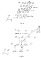
- Fig. 10 is a diagram for explaining a first method of the correcting process executed by the DSP circuit 46.
- pixels 70 are arranged in a grid shape in integer positions on the XY coordinates.
- the diagram illustrates an example of the movement of only one pixel in the process of the operation and shows that the value of an R signal (hereinafter, referred to as "R value”) Hd as the value of a pixel on the coordinates (1, 1) before the correcting operation by the DSP circuit 46 is moved to the coordinates (3, 4) after the operation.
- R value an R signal
- the movement amount of the R value by a vector (Fd, Gd).
- this can be explained as follows: if the coordinates of the pixel after the operation is (Xd, Yd), the pixel is a copy of the R value Hd in the coordinates (Xd - Fd, Yd - Gd).
- the movement amount (Fd, Gd) corresponding to each pixel after the operation is sufficient for the correction data to be stored in the correction data memory 42.
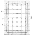
- FIG. 11 shows how to obtain the R value Hd of the pixel after the operation when the correction data in the coordinates (Xd, Yd), that is, the movement amount (Fd, Gd) is given in a real number.
- Coordinates (Ud, Vd) of a pixel to be referred to before the operation are given by the following expression (1).
- (Ud, Vd) (Xd - Fd, Yd - Gd)
- the above-mentioned correcting method will be examined in detail.
- the pixel values (H00, H10, H01, H11) used to estimate the R values are selected and determined by the integer parts in respective values of the movement amount (Fd, Gd) as correction data and the coefficient multiplied by each pixel value in the expression (2) (for example, the coefficient of H00 is (U1 - Ud) ⁇ (V1 - Vd)) is determined by the decimal fraction part of the movement amount.
- the estimating method is not limited to the above method but other calculating methods can be also used.
- the correction data is interpreted as a relative difference in coordinates used to refer to the pixel value which has not been subjected to the operation.
- the pixel value Hd in imaginary coordinates (Ud, Vd) is estimated, and then the pixel value is moved to the corrected coordinates (Xd, Yd).
- the pixel value is moved by the movement amount (Fd, Gd), and then the pixel value Hd which has been subjected to the operation is allocated to the four points near the coordinates after the movement.
- the program to execute the operation becomes slightly complicated.
- this method can be obviously used.
- the movement amount (Fd, Gd) as correction data is defined with respect to the three colors RGB of each pixel. If the correction data is set for all of the pixels, the total data amount therefore becomes too large to be ignored, and a memory of a large capacity to store the correction data becomes necessary. This causes the cost increase of the apparatus. Considerable working time is also required to measure the image distortion amount of the CRT 10a and the misconvergence amount with respect to all of the pixels on the correction data forming apparatus 1 side, calculate the correction data, and supply the correction data to the image display apparatus 10 side. There is another method that utilizes the fact that the image distortion amount of the CRT 10a and the misconvergence amount do not fluctuate so much among pixels positioning close to each other.
- the entire screen region is divided into some regions, and the correction data is supplied to only representative pixels in each of the divided regions.
- the correction data supplied to the other pixels is obtained by estimating from the correction data of the representative pixels can be considered. This method contributes to the reduction of the total amount of the correction data and the working time.
- a third method of the correcting process in which the correcting process is executed by giving the correcting data only to the representative pixels, will now be described. Since the pixel movement in a divided region is determined by the movement amounts of the representative pixels, the positions of the representative pixels will be called control points hereinbelow.
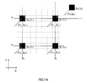
- Fig. 12 shows a case where the entire screen region on the frame memory 47 is divided into a plurality of rectangular regions and control points are set in a cross grating.
- the size of image information which is supplied is larger than the screen size actually displayed on the screen of the CRT 10a and the region called an over-scan region exists.
- the image region 90 of the frame memory 47 is usually set larger than the effective screen region 91 of the CRT 10a in consideration of the over-scan region.
- control points may be set in arbitrary positions outside the grid.
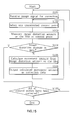
- Figs. 13 and 14 a method of obtaining the movement amount of an arbitrary pixel in each divided region when the control points are set in the grid as shown in Fig. 12 will be described.
- Fig. 13 is used to explain a method of obtaining the movement amount by interpolation.
- Fig. 14 is used to explain a method of obtaining the movement amount by extrapolation.
- the interpolation refers to a method of interpolating the movement amount of an arbitrary pixel positioning inside the region formed by linking a plurality of control points.
- the extrapolation refers to a method of interpolating the movement amount of an arbitrary pixel positioning outside the region formed by linking a plurality of control points.
- the movement amount can be obtained by the extrapolation with respect to all of the pixels, it is desirable that the extrapolation be used only with respect to pixels in the peripheral region of the screen (region idicated by shading with diagonal broken lines shown in Fig. 12).
- the extrapolation is used in the divided regions around the screen including the outer frame of the entire image region and the interpolation is used in the other region. Both in the interpolation and in the extrapolation, substantially the same calculating method can be used.
- the coordinates of the four control points denote the coordinates of the four control points by (X0, Y0), (X1, Y0), (X0, Y1), and (X1, Y1).
- the movement amounts corresponding to the correction data for the four control points be (F00, G00), (F10, G10), (F01, G01), and (F11, G11), respectively.
- the movement amount (Fd, Gd) of the pixel in arbitrary coordinates (Xd, Yd) can be given by the following equations (5) and (6). Those arithmetic expressions can be commonly used for the interpolation and extrapolation.
- the calculation shown by the expressions (5) and (6) is executed according to the method of estimation by linear interpolation.
- the estimation method is not, however, limited to the linear interpolation but other operation methods can be also used.
- An image signal for correction is supplied from the raster generating unit 12 to the image display apparatus 10 (step S101).
- the image signal for correction is, as shown in Fig. 12, for example, a signal of a grid image when displayed on the screen of the CRT 10a. In this case, the control points are positioned at the intersecting points of the grid.
- the image pickup apparatus 13 obtains an image for correction displayed on the screen on the CRT 10a and the obtained image data is stored into the frame memory 14 on the frame unit basis.
- the image data stored in the frame memory 14 is supplied to the image distortion data calculating unit 15.
- the image distortion data calculating unit 15 selects one uncorrected control point (step S102) and measures the image distortion amount or the misconvergence amount at the selected control point (step S103).
- the image distortion data calculating unit 15 determines whether the measured image distortion amount or the like is zero or not (step S104).
- the image distortion data calculating unit 15 calculates a movement amount required to correct the image distortion or the like (step S105) and outputs the calculated movement amount as correction data (step S106).
- the correction data outputted from the image distortion data calculating unit 15 is stored in the correction data memory 16 and transmitted to the image display apparatus 10 side.
- the transmitted correction data is stored into the correction data memory 42 via the external communication and writing unit 41.
- the correcting operation is performed by the DSP circuit 46 on the control point subject to the correction by using the correction data stored in the correction data memory 42.
- the image distortion data calculating unit 15 repeats the process of step S103 and subsequent processes for measuring again the image distortion amount or the misconvergence amount at the control point on which the correcting operation is performed. By repeating such processes until the image distortion amount or the like becomes small enough to be ignored, the correcting operation to the selected one control point is finished.
- the image distortion data calculating unit 15 determines whether the correcting operation with respect to all of the control points has been finished or not (step S107). When there is a control point which has not been subjected to the correcting operation yet (N in step S107), one of the uncorrected control points is selected and the process in step S102 and subsequent processes are repeated. When the correcting operation to all of the control points is finished (Y in step S107), the process is finished.
- the correction data for correcting the display state of the image on the basis of the image displayed on the screen is formed by the correcting data forming apparatus 1.
- the operation of correcting the image data is performed so that the image is properly displayed on the image display apparatus 10 side on the basis of the correction data, and the corrected image data is outputted to the CRT 10a.
- the image distortion and the misconvergence can be reduced more as compared with the related art of adjusting the image by using the deflecting yoke or the like.
- the related art in order to eliminate the image distortion or the like by the deflecting yoke, it is necessary to distort the deflecting magnetic field.
- the embodiment it is unnecessary to eliminate the image distortion or the like by the magnetic field of the deflecting yoke.
- the deflecting magnetic fields can therefore remain uniform, and thus the focus characteristics can be improved.
- the manufacturing cost and manufacturing time of the image display apparatus 10 can be reduced as compared with the adjustment in the method of the related art.
- the deflecting yoke is used to correct and adjust the image distortion or the like and thus the period for developing and designing the deflecting yoke is needed.
- the correction amount of the image distortion or the like is not so large, it is necessary to suppress variations in the assembly of the CRT and the deflecting yoke in order to suppress the image distortion or the like caused by the manufacturing variations of the CRT and the deflecting yoke to a certain extent.
- the correction amount of the image distortion or the like is large and thus the less accuracy in the assembly of the CRT and the deflecting yoke is required. Accordingly, the reduction of the manufacturing cost can be also expected.
- the influence by the external magnetic field such as the earth magnetism is known in advance, the information can be used as correction data, so that the image display apparatus having more excellent characteristics can be constructed.
- a defective display state such as the image distortion or the like is corrected at low cost and a high quality image can be displayed.
- the image distortion on a CRT whose angle is becoming wider in recent years or a flat CRT can be also optimally corrected.
- Fig. 16 is a block diagram showing a schematic construction of an image display apparatus according to the form of the second execution of the invention.
- the image display apparatus shown in the diagram comprises: an A/D converter 20 (20R, 20G, 20B) for converting inputted analog component video signals of colors R, G, and B into digital signals color by color and outputting the digital signals; a frame memory 21 (21R, 21G, 21B) for storing the digital signal of each color outputted from the A/D converter 20 on a frame unit basis; a correction write address generating unit 25 (25R, 25G, 25B) for controlling an address position on the frame memory 21 when the image data outputted from the A/D converter 20 is stored into the frame memory 21; a timing generator 23 for controlling the timing at which data is written by the correction write address generating unit 25; a read address generator 24 for generating an address signal SR for reading the data stored in the frame memory 21; and a D/A converter 22 (22R, 22G, 22B) for converting the digital signal for each color
- the frame memory 21 is a dual type memory to/from which data can be written/read.
- the frame memory 21 corresponds to the frame memories 45 and 47 shown in Fig. 5.
- the correction write address generating unit 25 corresponds to the DSP circuit 46 shown in Fig. 5.
- the correction write address generating unit 25 generates a write address signal SW to the frame memory 21 on the basis of the correction data outputted from the correction data forming apparatus 1 (Fig. 4) side.
- the image data outputted from the A/D converter 20 is stored in the address position instructed by the write address signal SW and is rearranged.
- the inputted image data is stored in a predetermined address position instructed by the write address signal SW in the frame memory 21. Thereby the corrected image data is stored into the frame memory 21.
- the timing generator 23 and the read address generator 24 are controlled by clock control signals S 1 and S 2 from a system controller (not shown) which controls the timings of sync signals.
- the image data rewritten in the frame memory 21 based on the write address signal SW is read in response to an address signal SR from the read address generator 24 and outputted to the D/A converter 22.
- the image distortion or the like can be automatically corrected thereafter.
- the invention is not limited to the foregoing forms of execution but can be variously modified.
- the screen of the image display apparatus 10 for forming the correction data may be measured visually.
- an adjustment knob is provided in the image display apparatus 10. By adjusting the adjustment knob, the information measured visually can be directly set as correction data on the image display apparatus 10 side.
- the external communication and writing unit 41 (Fig. 5) and the like can be omitted from the construction.
- the input signal D IN is not limited to the analog composite signal.
- an RGB analog signal may be used as the input signal D IN .
- an RGB signal can be obtained without the composite/RGB converter 43 (Fig. 5).
- a digital signal as a signal used in a digital television or the like may be inputted as the input signal D IN .
- a digital signal can be directly obtained without the A/D converter 44 (Fig. 5).
- the frame memory 45 and subsequent components can have an almost similar circuit construction in the example of the circuit shown in Fig. 5.
- the frame memory 47 may be omitted from the construction and the image data outputted from the DSP circuit 46 may be supplied directly via the D/A converter 48 to the CRT 10a.
- the correcting operation is performed on inputted image data on the basis of the correction data for correcting a display state of an image, obtained based on an image displayed on the screen so that an image is properly displayed, and the corrected image data is outputted as image data for display.
- a defective display state such as image distortion is corrected at low cost and a high quality image can be displayed.
- a plurality of pixels in uncorrected image data are selected on the basis of an integer part of a movement amount in order to calculate one pixel value in corrected image data. Meanwhile a calculation value to calculate one pixel value for the selected plurality of pixels is determined on the basis of the decimal fraction part of the movement amount.
- a pixel value of each of a plurality of representative pixels in a corrected image data is calculated by using a value of a pixel in a position deviated only by the movement amount from the representative pixel in uncorrected image data, while a pixel value of each of the other pixels than the representative pixels in the corrected image data is calculated by using a value of a pixel in a position deviated only by the movement amount from a proper display position obtained by estimation from the movement amount of the representative pixel in the uncorrected image data. Consequently, the correction data is given only to the representative pixels and the correction data in the other pixels can be estimated from the correction data of the representative pixels. Thus, the total amount of the correction data can be reduced and the working time necessary for the correction can be shortened.
- the correcting operation is performed on inputted image data on the basis of correction data for correcting a display state of an image, obtained based on an image displayed on a screen so that an image can be properly displayed, and the corrected image data is outputted as image data for display.
- An image is displayed on the basis of the outputted image data for display. Consequently, a defective display state such as image distortion is corrected at low cost and a high quality image can be displayed.
- the correction data forming apparatus obtains an image displayed on the screen of the image display apparatus and forms correction data for correcting a display state of an image on the basis of the obtained image.
- the image display apparatus performs the correcting operation on the inputted image data on the basis of the correction data formed by the correction data forming apparatus so that an image is properly displayed, outputs the corrected image data as image data for display, and displays an image on the basis of the image data for display. Consequently, the correction data can be automatically produced, and the image can be automatically corrected on the basis of the correction data. Therefore, a defective display state such as image distortion is corrected at low cost, and the high quality image can be displayed is produced.
Landscapes
- Engineering & Computer Science (AREA)
- Multimedia (AREA)
- Signal Processing (AREA)
- Video Image Reproduction Devices For Color Tv Systems (AREA)
- Controls And Circuits For Display Device (AREA)
- Details Of Television Scanning (AREA)
Applications Claiming Priority (4)
| Application Number | Priority Date | Filing Date | Title |
|---|---|---|---|
| JP24347098 | 1998-08-28 | ||
| JP24347098 | 1998-08-28 | ||
| JP1757299 | 1999-01-26 | ||
| JP01757299A JP3395832B2 (ja) | 1998-08-28 | 1999-01-26 | 画像表示補正システム、画像表示補正装置および方法並びに画像表示装置および方法 |
Publications (2)
| Publication Number | Publication Date |
|---|---|
| EP0982934A2 true EP0982934A2 (fr) | 2000-03-01 |
| EP0982934A3 EP0982934A3 (fr) | 2001-05-16 |
Family
ID=26354123
Family Applications (1)
| Application Number | Title | Priority Date | Filing Date |
|---|---|---|---|
| EP99402126A Withdrawn EP0982934A3 (fr) | 1998-08-28 | 1999-08-26 | Dispositif et méthode de correction de distorsion de balayage pour tubes à rayons cathodiques |
Country Status (6)
| Country | Link |
|---|---|
| US (1) | US6480242B1 (fr) |
| EP (1) | EP0982934A3 (fr) |
| JP (1) | JP3395832B2 (fr) |
| KR (1) | KR20000017582A (fr) |
| CN (1) | CN1250999A (fr) |
| TW (1) | TW448685B (fr) |
Cited By (3)
| Publication number | Priority date | Publication date | Assignee | Title |
|---|---|---|---|---|
| EP1827007A3 (fr) * | 2006-02-28 | 2007-12-26 | Samsung Electronics Co., Ltd. | Appareil et procédé d'affichage vidéo |
| WO2008115464A1 (fr) * | 2007-03-15 | 2008-09-25 | Scalable Display Technologies, Inc. | Système et procédé pour fournir une qualité d'affichage améliorée par ajustement d'affichage et traitement d'image en utilisant une rétroaction optique |
| US10319137B2 (en) | 2009-06-18 | 2019-06-11 | Scalable Display Technologies, Inc. | System and method for injection of mapping functions |
Families Citing this family (25)
| Publication number | Priority date | Publication date | Assignee | Title |
|---|---|---|---|---|
| US6538691B1 (en) * | 1999-01-21 | 2003-03-25 | Intel Corporation | Software correction of image distortion in digital cameras |
| JP3187787B2 (ja) | 1999-05-26 | 2001-07-11 | ソニー株式会社 | 画像制御装置および方法並びに画像表示装置 |
| KR100414083B1 (ko) * | 1999-12-18 | 2004-01-07 | 엘지전자 주식회사 | 영상왜곡 보정방법 및 이를 이용한 영상표시기기 |
| KR20030065310A (ko) * | 2000-04-05 | 2003-08-06 | 제네시스 마이크로칩 인코포레이티드 | 디스플레이에서의 에러를 정정하는 방법 및 장치 |
| JP2001309398A (ja) * | 2000-04-18 | 2001-11-02 | Sony Corp | 画像表示装置及び画像表示装置の地磁気による画像の傾き補正方法 |
| JP2001333434A (ja) * | 2000-05-19 | 2001-11-30 | Sony Corp | 画像処理装置および方法、並びに記録媒体 |
| JP2002112069A (ja) | 2000-07-25 | 2002-04-12 | Matsushita Electric Ind Co Ltd | 画像歪補正装置および画像歪補正方法 |
| JP2002094896A (ja) | 2000-09-13 | 2002-03-29 | Sony Corp | 陰極線管および輝度制御方法 |
| JP3675357B2 (ja) * | 2001-05-16 | 2005-07-27 | ソニー株式会社 | レジストレーション調整装置及びレジストレーション調整方法 |
| TW536910B (en) * | 2001-11-21 | 2003-06-11 | Eerise Corp | Image distortion correction method and device |
| JP3742027B2 (ja) * | 2002-04-08 | 2006-02-01 | Necビューテクノロジー株式会社 | 投射映像の歪補正方法、歪補正プログラム及び投射型映像表示装置 |
| CN100365658C (zh) * | 2002-06-12 | 2008-01-30 | 奥普提克斯晶硅有限公司 | 用于光学异常的电子校正的系统和方法 |
| JP4196274B2 (ja) * | 2003-08-11 | 2008-12-17 | ソニー株式会社 | 画像信号処理装置および方法、プログラム、並びに記録媒体 |
| US7227592B2 (en) * | 2003-09-26 | 2007-06-05 | Mitsubishi Electric Research Laboratories, Inc. | Self-correcting rear projection television |
| US7358877B1 (en) * | 2005-10-12 | 2008-04-15 | Advanced Testing Technologies, Inc. | Obsolescence mitigation for electron bombarded semiconductor tubes in programmable waveform digitizers |
| US7642940B1 (en) | 2005-10-12 | 2010-01-05 | Advanced Testing Technologies, Inc. | Obsolescence mitigation for programmable waveform digitizers |
| JP4344888B2 (ja) * | 2005-12-09 | 2009-10-14 | 株式会社カシオ日立モバイルコミュニケーションズ | 撮像装置、撮像画像処理方法及びプログラム |
| WO2007124450A2 (fr) * | 2006-04-21 | 2007-11-01 | The Trustees Of The University Of Pennsylvania | Compensation d'artefact de mouvement |
| JP4816569B2 (ja) * | 2006-07-06 | 2011-11-16 | セイコーエプソン株式会社 | 画像表示システム |
| JP2008197829A (ja) * | 2007-02-09 | 2008-08-28 | Sony Corp | 画像処理装置と方法およびプログラムと記録媒体 |
| JP5298507B2 (ja) | 2007-11-12 | 2013-09-25 | セイコーエプソン株式会社 | 画像表示装置及び画像表示方法 |
| TWI368752B (en) * | 2008-04-29 | 2012-07-21 | Wistron Corp | Video calibration system capable of performing automatic calibration and related method |
| JP5200743B2 (ja) | 2008-08-01 | 2013-06-05 | セイコーエプソン株式会社 | 画像処理装置、画像表示装置、画像処理方法、画像表示方法及びプログラム |
| CN103702181A (zh) * | 2013-12-13 | 2014-04-02 | 乐视网信息技术(北京)股份有限公司 | 一种视频图像的处理方法和装置 |
| JP6834542B2 (ja) * | 2017-02-01 | 2021-02-24 | セイコーエプソン株式会社 | 画像表示装置およびその調整方法 |
Family Cites Families (11)
| Publication number | Priority date | Publication date | Assignee | Title |
|---|---|---|---|---|
| JPS55163988A (en) | 1979-06-07 | 1980-12-20 | Nippon Hoso Kyokai <Nhk> | Digital convergence unit |
| FR2652695B1 (fr) * | 1989-10-03 | 1993-04-16 | Thomson Csf | Procede et dispositif de visualisation d'images, a correction automatique de defauts par contre-reaction. |
| JP3409330B2 (ja) * | 1991-02-08 | 2003-05-26 | ソニー株式会社 | 投射型表示装置の調整装置および調整方法 |
| GB2256989B (en) * | 1991-06-21 | 1995-02-08 | Sony Broadcast & Communication | Video image capture apparatus |
| JP3352468B2 (ja) | 1992-05-27 | 2002-12-03 | 三菱電機株式会社 | コンバーゼンス自動調整装置 |
| JPH06269014A (ja) | 1993-03-17 | 1994-09-22 | Matsushita Electric Ind Co Ltd | 画像補正装置 |
| US5465121A (en) * | 1993-03-31 | 1995-11-07 | International Business Machines Corporation | Method and system for compensating for image distortion caused by off-axis image projection |
| JPH07212779A (ja) | 1994-01-26 | 1995-08-11 | Toshiba Corp | デジタルコンバーゼンス装置 |
| KR0130871B1 (ko) * | 1994-03-21 | 1998-04-21 | 김광호 | 디지탈 콘버젼스 보정방법 및 장치 |
| JPH089405A (ja) * | 1994-06-22 | 1996-01-12 | Toshiba Corp | ディジタルコンバーゼンス装置 |
| EP0968515A1 (fr) | 1997-12-23 | 2000-01-05 | Koninklijke Philips Electronics N.V. | Tube cathodique en couleur a au moins deux bobines de deviation et deux canons a electrons |
-
1999
- 1999-01-26 JP JP01757299A patent/JP3395832B2/ja not_active Expired - Fee Related
- 1999-08-20 TW TW088114270A patent/TW448685B/zh not_active IP Right Cessation
- 1999-08-26 EP EP99402126A patent/EP0982934A3/fr not_active Withdrawn
- 1999-08-27 US US09/384,204 patent/US6480242B1/en not_active Expired - Fee Related
- 1999-08-27 KR KR1019990035815A patent/KR20000017582A/ko not_active Withdrawn
- 1999-08-28 CN CN99122028A patent/CN1250999A/zh active Pending
Cited By (9)
| Publication number | Priority date | Publication date | Assignee | Title |
|---|---|---|---|---|
| EP1827007A3 (fr) * | 2006-02-28 | 2007-12-26 | Samsung Electronics Co., Ltd. | Appareil et procédé d'affichage vidéo |
| WO2008115464A1 (fr) * | 2007-03-15 | 2008-09-25 | Scalable Display Technologies, Inc. | Système et procédé pour fournir une qualité d'affichage améliorée par ajustement d'affichage et traitement d'image en utilisant une rétroaction optique |
| US8994757B2 (en) | 2007-03-15 | 2015-03-31 | Scalable Display Technologies, Inc. | System and method for providing improved display quality by display adjustment and image processing using optical feedback |
| US10523910B2 (en) | 2007-03-15 | 2019-12-31 | Scalable Display Technologies, Inc. | System and method for providing improved display quality by display adjustment and image processing using optical feedback |
| US11159774B2 (en) | 2007-03-15 | 2021-10-26 | Scalable Display Technologies, Inc. | System and method for providing improved display quality by display adjustment and image processing using optical feedback |
| US11570412B2 (en) | 2007-03-15 | 2023-01-31 | Scalable Display Technologies, Inc. | System and method for providing improved display quality by display adjustment and image processing using optical feedback |
| US11930304B2 (en) | 2007-03-15 | 2024-03-12 | Scalable Display Technologies, Inc. | System and method for providing improved display quality by display adjustment and image processing using optical feedback |
| US12425552B2 (en) | 2007-03-15 | 2025-09-23 | Scalable Display Technologies, Inc. | System and method for providing improved display quality by display adjustment and image processing using optical feedback |
| US10319137B2 (en) | 2009-06-18 | 2019-06-11 | Scalable Display Technologies, Inc. | System and method for injection of mapping functions |
Also Published As
| Publication number | Publication date |
|---|---|
| EP0982934A3 (fr) | 2001-05-16 |
| TW448685B (en) | 2001-08-01 |
| JP3395832B2 (ja) | 2003-04-14 |
| JP2000138946A (ja) | 2000-05-16 |
| US6480242B1 (en) | 2002-11-12 |
| CN1250999A (zh) | 2000-04-19 |
| KR20000017582A (ko) | 2000-03-25 |
Similar Documents
| Publication | Publication Date | Title |
|---|---|---|
| US6480242B1 (en) | Image display correcting system, image display correcting apparatus and method, and image display apparatus and method | |
| US5298985A (en) | Image correction apparatus for adjusting images by digitially controlling analog correction waveforms | |
| US5796425A (en) | Elimination of the effect of difference in vertical scanning frequency between a display and a camera imaging the display | |
| US5497054A (en) | Automatic digital convergence correcting method and apparatus therefor | |
| JPH04216275A (ja) | ラスタひずみ補正回路 | |
| US6437522B1 (en) | Method for controlling digital dynamic convergence and system thereof | |
| KR20010007101A (ko) | 화상 제어 장치 및 방법 및 화상 표시 장치 | |
| US6580233B2 (en) | Cathode ray tube and intensity controlling method | |
| JP3178526B2 (ja) | 画像補正装置および方法並びに画像表示装置 | |
| KR20030042514A (ko) | Crt 화상장치의 디지털 동적 컨버전스 제어 시스템 | |
| JPS631792B2 (fr) | ||
| US20020024478A1 (en) | Cathode ray tube and image control device | |
| JPH0126234B2 (fr) | ||
| JP3675357B2 (ja) | レジストレーション調整装置及びレジストレーション調整方法 | |
| JP3057230B1 (ja) | 画像補正装置および方法並びに画像表示装置 | |
| JPH07264608A (ja) | コンバージェンス調整回路 | |
| JPH0583749A (ja) | ユニフオミテイ補正装置 | |
| JPS6163177A (ja) | デイジタルコンバ−ゼンス装置 | |
| KR20010014996A (ko) | 음극선관 및 휘도 조절 장치 및 그 방법 | |
| JP2001042848A (ja) | 画像制御装置および方法並びに画像表示装置 | |
| JPH0767123A (ja) | ディジタルコンバーゼンス装置 | |
| JPH11122562A (ja) | 画像補正装置 | |
| JPS6412437B2 (fr) | ||
| KR20030010809A (ko) | 디지털 컨버젼스 보정 방식 을 사용한 기하왜 보정 방법 | |
| JPH09247695A (ja) | ディジタル画像補正装置、及びその演算方法 |
Legal Events
| Date | Code | Title | Description |
|---|---|---|---|
| PUAI | Public reference made under article 153(3) epc to a published international application that has entered the european phase |
Free format text: ORIGINAL CODE: 0009012 |
|
| AK | Designated contracting states |
Kind code of ref document: A2 Designated state(s): DE FR GB |
|
| AX | Request for extension of the european patent |
Free format text: AL;LT;LV;MK;RO;SI |
|
| PUAL | Search report despatched |
Free format text: ORIGINAL CODE: 0009013 |
|
| AK | Designated contracting states |
Kind code of ref document: A3 Designated state(s): AT BE CH CY DE DK ES FI FR GB GR IE IT LI LU MC NL PT SE |
|
| AX | Request for extension of the european patent |
Free format text: AL;LT;LV;MK;RO;SI |
|
| 17P | Request for examination filed |
Effective date: 20011114 |
|
| 17Q | First examination report despatched |
Effective date: 20011221 |
|
| AKX | Designation fees paid |
Free format text: DE FR GB |
|
| STAA | Information on the status of an ep patent application or granted ep patent |
Free format text: STATUS: THE APPLICATION IS DEEMED TO BE WITHDRAWN |
|
| 18D | Application deemed to be withdrawn |
Effective date: 20030301 |