EP0996313A2 - Beleuchteter Schalter - Google Patents
Beleuchteter Schalter Download PDFInfo
- Publication number
- EP0996313A2 EP0996313A2 EP99124542A EP99124542A EP0996313A2 EP 0996313 A2 EP0996313 A2 EP 0996313A2 EP 99124542 A EP99124542 A EP 99124542A EP 99124542 A EP99124542 A EP 99124542A EP 0996313 A2 EP0996313 A2 EP 0996313A2
- Authority
- EP
- European Patent Office
- Prior art keywords
- lighting element
- printed
- switch unit
- layer
- accordance
- Prior art date
- Legal status (The legal status is an assumption and is not a legal conclusion. Google has not performed a legal analysis and makes no representation as to the accuracy of the status listed.)
- Withdrawn
Links
Images



Classifications
-
- H—ELECTRICITY
- H05—ELECTRIC TECHNIQUES NOT OTHERWISE PROVIDED FOR
- H05B—ELECTRIC HEATING; ELECTRIC LIGHT SOURCES NOT OTHERWISE PROVIDED FOR; CIRCUIT ARRANGEMENTS FOR ELECTRIC LIGHT SOURCES, IN GENERAL
- H05B33/00—Electroluminescent light sources
-
- H—ELECTRICITY
- H01—ELECTRIC ELEMENTS
- H01H—ELECTRIC SWITCHES; RELAYS; SELECTORS; EMERGENCY PROTECTIVE DEVICES
- H01H13/00—Switches having rectilinearly-movable operating part or parts adapted for pushing or pulling in one direction only, e.g. push-button switch
- H01H13/70—Switches having rectilinearly-movable operating part or parts adapted for pushing or pulling in one direction only, e.g. push-button switch having a plurality of operating members associated with different sets of contacts, e.g. keyboard
- H01H13/702—Switches having rectilinearly-movable operating part or parts adapted for pushing or pulling in one direction only, e.g. push-button switch having a plurality of operating members associated with different sets of contacts, e.g. keyboard with contacts carried by or formed from layers in a multilayer structure, e.g. membrane switches
-
- H—ELECTRICITY
- H05—ELECTRIC TECHNIQUES NOT OTHERWISE PROVIDED FOR
- H05B—ELECTRIC HEATING; ELECTRIC LIGHT SOURCES NOT OTHERWISE PROVIDED FOR; CIRCUIT ARRANGEMENTS FOR ELECTRIC LIGHT SOURCES, IN GENERAL
- H05B33/00—Electroluminescent light sources
- H05B33/10—Apparatus or processes specially adapted to the manufacture of electroluminescent light sources
-
- H—ELECTRICITY
- H05—ELECTRIC TECHNIQUES NOT OTHERWISE PROVIDED FOR
- H05B—ELECTRIC HEATING; ELECTRIC LIGHT SOURCES NOT OTHERWISE PROVIDED FOR; CIRCUIT ARRANGEMENTS FOR ELECTRIC LIGHT SOURCES, IN GENERAL
- H05B33/00—Electroluminescent light sources
- H05B33/12—Light sources with substantially two-dimensional [2D] radiating surfaces
-
- H—ELECTRICITY
- H05—ELECTRIC TECHNIQUES NOT OTHERWISE PROVIDED FOR
- H05B—ELECTRIC HEATING; ELECTRIC LIGHT SOURCES NOT OTHERWISE PROVIDED FOR; CIRCUIT ARRANGEMENTS FOR ELECTRIC LIGHT SOURCES, IN GENERAL
- H05B33/00—Electroluminescent light sources
- H05B33/12—Light sources with substantially two-dimensional [2D] radiating surfaces
- H05B33/26—Light sources with substantially two-dimensional [2D] radiating surfaces characterised by the composition or arrangement of the conductive material used as an electrode
- H05B33/28—Light sources with substantially two-dimensional [2D] radiating surfaces characterised by the composition or arrangement of the conductive material used as an electrode of translucent electrodes
-
- H—ELECTRICITY
- H10—SEMICONDUCTOR DEVICES; ELECTRIC SOLID-STATE DEVICES NOT OTHERWISE PROVIDED FOR
- H10K—ORGANIC ELECTRIC SOLID-STATE DEVICES
- H10K59/00—Integrated devices, or assemblies of multiple devices, comprising at least one organic light-emitting element covered by group H10K50/00
- H10K59/80—Constructional details
- H10K59/805—Electrodes
- H10K59/8051—Anodes
-
- H—ELECTRICITY
- H01—ELECTRIC ELEMENTS
- H01H—ELECTRIC SWITCHES; RELAYS; SELECTORS; EMERGENCY PROTECTIVE DEVICES
- H01H2219/00—Legends
- H01H2219/002—Legends replaceable; adaptable
- H01H2219/018—Electroluminescent panel
-
- H—ELECTRICITY
- H01—ELECTRIC ELEMENTS
- H01H—ELECTRIC SWITCHES; RELAYS; SELECTORS; EMERGENCY PROTECTIVE DEVICES
- H01H2219/00—Legends
- H01H2219/028—Printed information
-
- H—ELECTRICITY
- H01—ELECTRIC ELEMENTS
- H01H—ELECTRIC SWITCHES; RELAYS; SELECTORS; EMERGENCY PROTECTIVE DEVICES
- H01H2219/00—Legends
- H01H2219/036—Light emitting elements
- H01H2219/046—Light emitting elements above switch site
-
- H—ELECTRICITY
- H01—ELECTRIC ELEMENTS
- H01H—ELECTRIC SWITCHES; RELAYS; SELECTORS; EMERGENCY PROTECTIVE DEVICES
- H01H2221/00—Actuators
- H01H2221/05—Force concentrator; Actuating dimple
-
- H—ELECTRICITY
- H10—SEMICONDUCTOR DEVICES; ELECTRIC SOLID-STATE DEVICES NOT OTHERWISE PROVIDED FOR
- H10K—ORGANIC ELECTRIC SOLID-STATE DEVICES
- H10K2102/00—Constructional details relating to the organic devices covered by this subclass
- H10K2102/10—Transparent electrodes, e.g. using graphene
- H10K2102/101—Transparent electrodes, e.g. using graphene comprising transparent conductive oxides [TCO]
- H10K2102/102—Transparent electrodes, e.g. using graphene comprising transparent conductive oxides [TCO] comprising tin oxides, e.g. fluorine-doped SnO2
-
- H—ELECTRICITY
- H10—SEMICONDUCTOR DEVICES; ELECTRIC SOLID-STATE DEVICES NOT OTHERWISE PROVIDED FOR
- H10K—ORGANIC ELECTRIC SOLID-STATE DEVICES
- H10K50/00—Organic light-emitting devices
- H10K50/80—Constructional details
- H10K50/805—Electrodes
- H10K50/81—Anodes
-
- H—ELECTRICITY
- H10—SEMICONDUCTOR DEVICES; ELECTRIC SOLID-STATE DEVICES NOT OTHERWISE PROVIDED FOR
- H10K—ORGANIC ELECTRIC SOLID-STATE DEVICES
- H10K59/00—Integrated devices, or assemblies of multiple devices, comprising at least one organic light-emitting element covered by group H10K50/00
- H10K59/80—Constructional details
- H10K59/87—Passivation; Containers; Encapsulations
- H10K59/871—Self-supporting sealing arrangements
- H10K59/8723—Vertical spacers, e.g. arranged between the sealing arrangement and the OLED
Definitions
- the present invention relates to an illuminated switch unit using an EL lighting element preferably applicable to input operating sections of various electronic devices.
- Recent developments of micro IC drive inverters have increased the need for an EL lighting element which is thin and capable of realizing a proper surface lighting serving as a backlight for liquid crystal display units and switches of various electronic components, such as communication devices, video devices, and acoustic devices.
- an upper insulating sheet 201 made of resin film has a reverse surface on which a movable contact 202 is printed.
- a lower insulating sheet 203 has an upper surface on which a stationary contact 204 is printed.
- Spacer 205 which is resin film having both surfaces applied with adhesive, are interposed between upper insulating sheet 201 and lower insulating sheet 203 so that movable contact 202 and stationary contact 204 are disposed in a confronting relationship with a predetermined gap therebetween when these sheets 201 and 203 are fixed each other to form a membrane switch 206.
- An electroluminescent lighting element (abbreviated as EL lighting element) 207 is disposed on this membrane switch 206.
- a top sheet 211 made of transparent resin film, is disposed and fixed on this EL lighting element 207 via spacer 212 of transparent resin film applied adhesive on both surfaces thereof.
- Top sheet 211 has an upper surface provided with printed pattern representing letters, figures or others 208 and a lower surface provided with a button 209 which is a transparent or semi-transparent resin product bonded by adhesive 210 to the lower surface of top sheet 211, thereby constituting the conventional illuminated switch unit.
- Depressing top sheet 211 causes button 209 to move downward and press or push EL lighting element 207.
- a region of upper insulating sheet 201 which received a depressing force through EL lighting element 207 is recessed.
- Movable contact 202 which constitutes part of membrane switch 206 and is provided at the lower surface of the recessed portion of upper insulating sheet 201, is depressed downward.
- movable contact 202 can be brought into contact with stationary contact 204 provided on lower insulating sheet 203, thereby establishing an electrical connection therebetween.
- button 209 and spacer 212 causes undesirable illumination such as silhouette of these parts or irregularities of luminance. Furthermore, the manufacturing costs will be increased due to numerous parts and increased assembling processes.
- US 4,537,395 discloses a membrane switch having an electroluminescent lighting element provided directly on the flexible membrane of the switch.
- the present invention aims to provide an illuminated switch unit capable of improving uniformity of illumination from the EL lighting element, simple in construction, and cheap in manufacturing costs.
- the present invention provides an illuminated switch unit comprising an EL lighting element having a reverse surface provided with a switch operating projection which constitutes an operating means be disposed above a push switch.
- an illuminated switch unit comprising:
- the electroluminescent lighting element is a diffusion-type electroluminescent lighting element. Furthermore, it is preferable that a surface of the electroluminescent lighting element, serving as a light-emitting surface, is provided with printed pattern representing letters, figures or others.
- the push switch may be a membrane switch with or without click motion.
- the push switch may be a push switch with click motion, and the movable contact may be a metallic thin plate configured in a diaphragm shape.
- An insulating transparent film 1 is a polyethylene terephthalate (abbreviated as PET, hereinafter) film of 75 ⁇ m.
- a transparent electrode layer 2 having a dry film thickness of 3 to 5 ⁇ m is pattern printed on this insulating transparent film 1 by screen printing a transparent electrode paste.
- This transparent electrode paste is produced by the following procedure. First, thermal-hardening insulating resin (which is formed by mixing epoxy resin #828 commercially available from Yuka Shell Co., Ltd. and phenoxy resin YP-40 commercially available from Touto Kasei Co., Ltd. at the same weight ratio and then adding imidazole block isocyanate G8009B commercially available from Daiichi Kogyo Seiyaku Co., Ltd.
- the following pastes are successively accumulated on the transparent electrode layer 2 at predetermined patterns to form a multi-layer construction of light-emitting layer 3, dielectric layer 4, back-surface electrode layer 5, and insulating coat layer 6.
- Light-emitting layer 3 a paste forming the light-emitting layer 3 is produced by the following procedure.
- a mixed solution of 50g, consisting of cyanoethyl pullulan resin of 70 weight % and cyanoethyl polyvinyl alcohol resin of 30 weight % i.e. a solution obtained by dissolving CR-M of 30 weight % with formamide; CR-M is a product commercially available from Shin-etsu Chemical Co., Ltd.
- imidazole block isocyanate G8009B supplied by Daiichi Kogyo Seiyaku Co., Ltd.
- illuminant TYPE40 of Sylvania Corporation
- a dry thickness of resultant light-emitting layer 3 was 35 ⁇ m.
- Dielectric layer 4 a paste forming the dielectric layer 4 is produced by the following procedure. That is, vinylidene fluoride copolymer rubber solution of 53g (a solution obtained by dissolving DAIEL G902 of 35 weight % with isophorone; Daiel G902 is a commercially available product from Daikin Industry Co., Ltd.) is mixed with the hardening agent consisting of 0.02g Di-cumyl peroxide and 50g BaTiO 3 powder (commercially available from Kantou Chemical Co., Ltd.) by performing the three-roll diffusing operation. Thus formed paste had a dry film thickness of 35 ⁇ m.
- vinylidene fluoride copolymer rubber solution of 53g a solution obtained by dissolving DAIEL G902 of 35 weight % with isophorone; Daiel G902 is a commercially available product from Daikin Industry Co., Ltd.
- the hardening agent consisting of 0.02g Di-cumyl peroxide and 50g BaTi
- Back-surface electrode layer 5 a paste forming the back-surface electrode layer 5 is a conductive paste (DW-250H of Toyobo Co., Ltd.) A resultant film had a dry thickness of 10 ⁇ m.
- Insulating coat layer 6 a paste forming the insulating coat layer 6 is an insulating paste (XB-804A of Fujikura Kasei Co., Ltd.). A resultant film had a dry film thickness of 30 ⁇ m.
- Fig. 1 shows a plan view showing the EL lighting element produced by performing the above-described lamination printing method.
- Fig. 2 is a cross-sectional view taken along a line X-Y of Fig. 1.
- collecting electrodes 5a and 5b are integrally formed with the back-surface electrode layer 5 by performing a simultaneous pattern printing operation.
- electric voltage 100V of 400Hz was applied on these collecting electrodes 5a and 5b, an initial luminance of 74.8 Cd/m 2 was obtained.
- the 50% luminance decline period was measured by leaving the light-emitting sample of this embodiment in a tank of 70°C and a tank of 40°C/90-95% RH.
- the 50% luminance decline period was 300 hours in the 70°C tank, and was the 1,000 hours in the 40°C/90-95% RH tank.
- the indium oxide powder serving as the conductive powder comprises needle-like powder (A) and fine-grain powder (B) blended at a predetermined weight ratio (A):(B).
- A needle-like powder
- B fine-grain powder
- the ratio of needle-like powder (A) is less than 20%, the conductivity is largely deteriorated in the lamination printing process of light-emitting layer 3 and dielectric layer 4 and also in the succeeding drying process. Hence, the luminance is lowered correspondingly. When this sample is left in an atmosphere of high temperature and high humidity, the luminance is further worsened.
- the ratio of all the conductive powder (C) to the insulating resin (D) is not larger than 45%, the conductivity is so declined that no light can be obtained from the EL lighting element and the dispersion of the luminance is enlarged.
- the ratio of all the conductive powder (C) to the insulating resin (D) is not less than 95%, it becomes impossible to obtain a uniform film layer in the printing operation. Hence, the light permeability is deteriorated. The luminance will be also deteriorated, and the dispersion of the luminance will be enlarged.
- the following is desirable ratios defined based on the experimental data.
- the thermal-hardening insulating resin contained in the transparent electrode paste, used in the first example was set to the same solid-state ratio.
- several EL lighting elements were experimentally fabricated by using various transparent electrode pastes including the following resins.
- Two comparative examples e) and g) caused no light emission.
- Another comparative example f) caused a small amount of light emission in the vicinity of collecting electrode 5a.
- the conductive power of the transparent electrode paste, used in a third example was a mixture of needle-like stannic indium oxide (SCP-SX of Sumitomo Metal Mining Co., Ltd.) and fine-grain stannic indium oxide (UFP-X of Sumitomo Metal Mining Co., Ltd.). And, its blending ratio was changed variously. Furthermore, the blending ratio of all the conductive powder to the insulating resin was also changed. Numerous EL lighting elements were fabricated by combining these two parameters in matrix. Then, luminance value, irregularities of luminance, and resistance value of the transparent electrode of each finished product of the fabricated EL lighting element were measured. Table 1 shows the result of the measurements.
- 0 to 100 wt% represents the ratio of the needle-like powder to all the conductive powder, while 30 to 96 % represents the blending ratio of all the conductive powder to the insulating resin.
- Infinity ( ⁇ ) represents a resistance value larger than 10M ⁇ , and " - " represents the experimental result that no paste was obtained and therefore no printing operation was performed.
- the luminance value is expressed in terms of Cd/m 2
- the resistance value is expressed in terms of k ⁇ .
- thermocompression bonding terminal 9 provided at the distal end of collecting electrodes 5a and 5b of the EL lighting element of the first example, was connected to a printed circuit board 10 by using anisotropic conductive adhesive (CP7131 of Sony Chemical Co., Ltd.) under thermocompression bonding conditions of 180°C, 35kg/cm 2 and 30sec.
- Fig. 3 shows a connected condition of thermocompression bonding terminal 9 and printed circuit board 10.
- a driving inverter circuit is mounted on printed circuit board 10 to activate or turn on a light-emitting section 7. Light-emitting condition was not at all changed by bending a wiring harness 8 of the collecting electrodes in any way.
- a reinforcement board 11 which is PET film of 188 ⁇ m with adhesive on its surface is bonded on the reverse surface of collecting electrodes 5a and 5b of the EL lighting element of the first embodiment, to fabricate an EL lighting element capable of connecting a film connector.
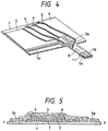
- Fig. 4 is a partly cross-sectional view showing each layer of the fifth example EL lighting element.
- the arrangement of collecting electrodes 5a and 5b, back-surface electrode layer 5 and insulating coat layer 6 are modified in the following manner.
- Collecting electrodes 5a and 5b conductive paste (DW-250H of Toyobo Co., Ltd.) having a dry film thickness of 10 ⁇ m.
- Back-surface electrode layer 5 conductive paste (DY-150H of Toyobo Co., Ltd.) having a dry film thickness of 8 ⁇ m.
- Insulating coat layer 6 insulating paste (TSE3221 of Toshiba Silicon Co., Ltd.) having a dry film thickness of 25 ⁇ m.
- Collecting electrodes 5a and 5b are silver resin group paste, while back-surface electrode layer 5 is carbon resin group paste.
- the EL lighting element of the present invention does not cause a deterioration of the conductivity of the transparent electrode layer even if the light-emitting layer and the dielectric layer are pattern printed in the piled-up manner on the transparent electrode layer.
- all of layers including the transparent electrode layer can be formed by (screen) printing. Hence, the production cost is cheap and electrical connection of the collecting electrodes can be easily done.
- a flexible printed circuit board is generally known as having a circuit wiring pattern printed by conductive paste on an insulating transparent film such as PET.
- the present invention makes it possible to form an EL lighting element at a desired portion on the FPC by pattern printing, bringing large merits in various industries.
- an EL lighting element 15 having a reverse surface provided with a switch operating projection 14 is disposed on a membrane switch 13 via spacer 16 which is an adhesive sheet made of resin film having a thickness of approximately 200 ⁇ m and having both surfaces applied adhesive thereon.
- An upper movable contact 21 is printed on a reverse (lower) surface of an upper insulating sheet 20, made of resin film having a thickness of approximately 100 ⁇ m, by using a silver resin group or carbon resin group paste, in such a manner that upper movable contact 21 is disposed in confronting relationship with lower stationary contact 18.
- An upper insulating spacer 22 is formed around this upper movable contact 21 using semi-transparent insulating paste so as to expose this movable contact 21.
- This transparent electrode paste contains indium oxide power added and diffused into insulating resin.
- a light-emitting layer 25 is printed on a lower surface of this transparent electrode layer 24 by using a paste containing zinc sulfide phosphor powder stirred and diffused into binder resin.
- a dielectric layer 26 is printed on a lower surface of this light-emitting layer 25 by using a paste containing barium titanate powder stirred and diffused into binder resin.
- a back-surface electrode layer 27 is printed on a lower surface of this dielectric layer 26 by using a carbon resin group paste.
- an insulating coat layer 28 is printed on a lower surface of this back-surface electrode layer 27 by using an insulating paste.
- a switch operating projection 14 is printed by using an epoxy group resin at a predetermined position on a lower surface of insulating coat layer 28, so that this switch operating projection 14 can be positioned concentrically with lower stationary contact 18 and upper movable contact 21 of membrane switch 13 when EL lighting element 15 is placed on membrane switch 13 by keeping back-surface electrode layer 28 at bottom.
- EL lighting element 15 Provided on an upper surface of EL lighting element 15 are printed patterns 48 representing letters, figures or others.
- the second embodiment is different from the first embodiment in that a movable contact 29 is provided on a lower surface of a diaphragm 30 configured or squeezed into a dome shape by thermally molding upper insulating sheet 20 of membrane switch 13.
- the third embodiment is different from the second embodiment in the arrangement of the membrane switch.
- an membrane switch 31 of this embodiment comprises a horseshoe-like stationary contact 33 which is a conductive pattern formed on a lower insulating substrate 32, a circular stationary contact 34 provided closely inside the horseshoe-like stationary contact 33, a saucer-like diaphragm 35 which is made of a metallic member having sufficient resilience such as phosphor spring or stainless steel, and an adhesive tape 36 which is a resin film having a surface applied with adhesive for bonding diaphragm 35 to stationary contact 33.
- EL lighting element 15 is fixedly provided above this membrane switch 31 through a spacer 37 which is an adhesive sheet made of resin film having a thickness of approximately 200 ⁇ m and having both surfaces applied adhesive thereon.
- the present invention forms the switch operating projection on the back-surface side of the EL lighting element and disposed this EL lighting element above the push switch. Hence, it becomes possible to remove any obstacles interrupting or intercepting illumination light emitted from the EL lighting element. Hence, uniformity of EL lighting element illumination can be surely obtained. Furthermore, the construction of the illuminated switch unit becomes so simple that a large number of parts and assembling processes can be eliminated. Accordingly, it becomes possible to provide a cheaper illuminated switch unit, bringing great utilities and merits in various industries.
Landscapes
- Engineering & Computer Science (AREA)
- Manufacturing & Machinery (AREA)
- Electroluminescent Light Sources (AREA)
- Push-Button Switches (AREA)
Applications Claiming Priority (6)
| Application Number | Priority Date | Filing Date | Title |
|---|---|---|---|
| JP7178499A JPH0935873A (ja) | 1995-07-14 | 1995-07-14 | Elランプおよびその製造方法 |
| JP17849995 | 1995-07-14 | ||
| JP7178490A JPH0935571A (ja) | 1995-07-14 | 1995-07-14 | 照光式スイッチユニット |
| JP17849095 | 1995-07-14 | ||
| EP96305101A EP0753985B1 (de) | 1995-07-14 | 1996-07-11 | Lumineszenzelement, Methode zur Herstellung desselben, und beleuchtetes Schaltelement damit |
| EP97109902A EP0801517A3 (de) | 1995-07-14 | 1996-07-11 | Beleuchteter Schalter |
Related Parent Applications (1)
| Application Number | Title | Priority Date | Filing Date |
|---|---|---|---|
| EP97109902A Division EP0801517A3 (de) | 1995-07-14 | 1996-07-11 | Beleuchteter Schalter |
Publications (2)
| Publication Number | Publication Date |
|---|---|
| EP0996313A2 true EP0996313A2 (de) | 2000-04-26 |
| EP0996313A3 EP0996313A3 (de) | 2000-08-02 |
Family
ID=26498662
Family Applications (3)
| Application Number | Title | Priority Date | Filing Date |
|---|---|---|---|
| EP97109902A Ceased EP0801517A3 (de) | 1995-07-14 | 1996-07-11 | Beleuchteter Schalter |
| EP99124542A Withdrawn EP0996313A3 (de) | 1995-07-14 | 1996-07-11 | Beleuchteter Schalter |
| EP96305101A Expired - Lifetime EP0753985B1 (de) | 1995-07-14 | 1996-07-11 | Lumineszenzelement, Methode zur Herstellung desselben, und beleuchtetes Schaltelement damit |
Family Applications Before (1)
| Application Number | Title | Priority Date | Filing Date |
|---|---|---|---|
| EP97109902A Ceased EP0801517A3 (de) | 1995-07-14 | 1996-07-11 | Beleuchteter Schalter |
Family Applications After (1)
| Application Number | Title | Priority Date | Filing Date |
|---|---|---|---|
| EP96305101A Expired - Lifetime EP0753985B1 (de) | 1995-07-14 | 1996-07-11 | Lumineszenzelement, Methode zur Herstellung desselben, und beleuchtetes Schaltelement damit |
Country Status (4)
| Country | Link |
|---|---|
| US (2) | US5844362A (de) |
| EP (3) | EP0801517A3 (de) |
| CN (1) | CN1138459C (de) |
| DE (1) | DE69606806T2 (de) |
Cited By (2)
| Publication number | Priority date | Publication date | Assignee | Title |
|---|---|---|---|---|
| LU90594B1 (de) * | 2000-06-09 | 2001-12-10 | Iee Sarl | Beleuchtetes Schaltelement |
| US9136492B2 (en) | 2009-03-18 | 2015-09-15 | Semiconductor Energy Laboratory Co., Ltd. | Lighting device with a connection structure and connecting member |
Families Citing this family (90)
| Publication number | Priority date | Publication date | Assignee | Title |
|---|---|---|---|---|
| JP3339554B2 (ja) | 1995-12-15 | 2002-10-28 | 松下電器産業株式会社 | プラズマディスプレイパネル及びその製造方法 |
| US6054809A (en) * | 1996-08-14 | 2000-04-25 | Add-Vision, Inc. | Electroluminescent lamp designs |
| US5797482A (en) * | 1996-11-25 | 1998-08-25 | Metro-Mark, Inc. | Electroluminescent keypad |
| JP3999837B2 (ja) * | 1997-02-10 | 2007-10-31 | Tdk株式会社 | 有機エレクトロルミネッセンス表示装置 |
| US6175345B1 (en) * | 1997-06-02 | 2001-01-16 | Canon Kabushiki Kaisha | Electroluminescence device, electroluminescence apparatus, and production methods thereof |
| ES2264208T3 (es) * | 1997-07-31 | 2006-12-16 | Toyotomi Co., Ltd. | Soluciones topicas que contienen centroprofeno estabilizado con sulisobenzona. |
| DE59802095D1 (de) * | 1997-10-13 | 2001-12-13 | Magna Auteca Ag Krottendorf | Leuchtvorrichtung |
| JP2850906B1 (ja) * | 1997-10-24 | 1999-01-27 | 日本電気株式会社 | 有機el素子およびその製造方法 |
| US5953587A (en) * | 1997-11-24 | 1999-09-14 | The Trustees Of Princeton University | Method for deposition and patterning of organic thin film |
| US6075316A (en) * | 1997-12-15 | 2000-06-13 | Motorola, Inc. | Full color organic electroluminescent display device and method of fabrication |
| EP0942445A1 (de) * | 1998-03-13 | 1999-09-15 | Koninklijke Philips Electronics N.V. | Kontaktfühlervorrichtung, Apparat zur Anwendung einer solchen Vorrichtung und Funktelefon mit einer solchen Vorrichtung |
| JP3556459B2 (ja) | 1998-03-13 | 2004-08-18 | セイコープレシジョン株式会社 | Elモジュール |
| US6106352A (en) * | 1998-03-18 | 2000-08-22 | Sanyo Electric Co., Ltd. | Method for fabrication of organic electroluminescent device |
| JP3110374B2 (ja) * | 1998-03-27 | 2000-11-20 | 静岡日本電気株式会社 | Elランプの取付構造 |
| US6624571B1 (en) * | 1998-06-30 | 2003-09-23 | Nippon Seiki Co., Ltd. | Electroluminescent display |
| AU9009898A (en) * | 1998-08-20 | 2000-03-14 | Screen Sign Arts Limited | Illuminated membrane switch |
| DE69828885T2 (de) * | 1998-12-02 | 2006-01-19 | Molex Inc., Lisle | "Elektrischer Sachlter mit beleuchteter Membran" |
| JP2001035652A (ja) | 1999-07-21 | 2001-02-09 | Matsushita Electric Ind Co Ltd | エレクトロルミネッセンス素子及びこれを用いた照光ユニット |
| DE60020859T2 (de) * | 1999-10-06 | 2006-05-11 | Allied Photochemical, Inc., Kimball | UV-Härtbare Zusammensetzungen zur Herstellung von Elektrolumineszenzbeschichtungen |
| US6677709B1 (en) * | 2000-07-18 | 2004-01-13 | General Electric Company | Micro electromechanical system controlled organic led and pixel arrays and method of using and of manufacturing same |
| JP2002299067A (ja) * | 2001-04-03 | 2002-10-11 | Matsushita Electric Ind Co Ltd | El素子及びこれを用いた照光装置 |
| JP2003007455A (ja) * | 2001-06-25 | 2003-01-10 | Alps Electric Co Ltd | エレクトロルミネッセント素子 |
| JP2005526353A (ja) * | 2001-07-27 | 2005-09-02 | ジ・オハイオ・ステート・ユニバーシティ | スクリーンプリンティング処理によるエレクトロルミネッセンスの製造法 |
| US6698085B2 (en) * | 2001-08-30 | 2004-03-02 | Novatech Electro-Luminescent, Inc. | Method for manufacturing low cost electroluminescent (EL) illuminated membrane switches |
| US7026758B2 (en) * | 2001-09-28 | 2006-04-11 | Osram Opto Semiconductors Gmbh | Reinforcement of glass substrates in flexible devices |
| AU2002361859A1 (en) * | 2001-12-20 | 2003-07-09 | Add-Vision, Inc. | Screen printable electrode for organic light emitting device |
| CN1219413C (zh) * | 2001-12-21 | 2005-09-14 | 深圳市威福玛实业有限公司 | 光显示扬声器 |
| US6565231B1 (en) * | 2002-05-28 | 2003-05-20 | Eastman Kodak Company | OLED area illumination lighting apparatus |
| US6787990B2 (en) * | 2002-05-28 | 2004-09-07 | Eastman Kodak Company | OLED area illumination light source having flexible substrate on a support |
| US7075025B2 (en) | 2002-08-09 | 2006-07-11 | Fujikura Ltd. | Switch sheet and switch |
| DE20212471U1 (de) | 2002-08-13 | 2003-02-06 | FER Fahrzeugelektrik GmbH, 99817 Eisenach | Beleuchtungsvorrichtung |
| US7098525B2 (en) * | 2003-05-08 | 2006-08-29 | 3M Innovative Properties Company | Organic polymers, electronic devices, and methods |
| US7279777B2 (en) * | 2003-05-08 | 2007-10-09 | 3M Innovative Properties Company | Organic polymers, laminates, and capacitors |
| US6874904B2 (en) * | 2003-05-21 | 2005-04-05 | Tai Ping Hsu | Light brightness changeable electroluminescent device |
| WO2004110892A1 (en) * | 2003-06-12 | 2004-12-23 | Benmore Ventures Ltd | Container with light or sound generator |
| JP2005071808A (ja) * | 2003-08-25 | 2005-03-17 | Citizen Electronics Co Ltd | キーシートモジュール |
| EP1720380B1 (de) * | 2004-02-26 | 2016-11-02 | Toshiba Materials Co., Ltd. | Schalterbeleuchtungs-el-blatt und beleuchtungsschalter und elektronische vorrichtung damit |
| JP2006156035A (ja) * | 2004-11-26 | 2006-06-15 | Toshiba Matsushita Display Technology Co Ltd | 表示装置 |
| EP1705960A1 (de) * | 2005-03-21 | 2006-09-27 | IEE INTERNATIONAL ELECTRONICS & ENGINEERING S.A. | Eletrolumineszierende Lampe |
| JP2006278244A (ja) * | 2005-03-30 | 2006-10-12 | Seiko Precision Inc | 照光式スイッチ |
| WO2006117717A2 (en) * | 2005-04-29 | 2006-11-09 | Philips Intellectual Property & Standards Gmbh | Electroluminescent device |
| DE102005025125B4 (de) * | 2005-05-29 | 2008-05-08 | Hahn-Meitner-Institut Berlin Gmbh | Verfahren zur Herstellung einer einseitig kontaktierten Solarzelle und einseitig kontaktierte Solarzelle |
| US7445350B2 (en) * | 2005-08-22 | 2008-11-04 | Nissan Technical Center North America, Inc. | Interior/exterior component with electroluminescent lighting and soft touch switching |
| JP2007173185A (ja) * | 2005-12-26 | 2007-07-05 | Polymatech Co Ltd | 照光式キーシート |
| CN101809691B (zh) * | 2007-04-20 | 2012-07-18 | 英克-罗吉克斯有限公司 | 模内成型的电容式开关 |
| US8198979B2 (en) | 2007-04-20 | 2012-06-12 | Ink-Logix, Llc | In-molded resistive and shielding elements |
| JP5005089B2 (ja) * | 2007-06-20 | 2012-08-22 | カーリング クリエイティブ コンサル株式会社 | 導光シートを使用した変換型キーパッドパッケージ |
| DE102007040889B3 (de) * | 2007-08-29 | 2008-12-11 | Siemens Home And Office Communication Devices Gmbh & Co. Kg | Tastaturmatte und elektrisches Gerät |
| GB0815897D0 (en) * | 2008-09-01 | 2008-10-08 | Benmore Ventures Ltd | Container illumination device |
| USD637750S1 (en) | 2008-09-08 | 2011-05-10 | Benmore Ventures Ltd | Light-emitting unit for bottles and other containers |
| US8853820B2 (en) | 2009-05-25 | 2014-10-07 | Basf Se | Crosslinkable dielectrics and methods of preparation and use thereof |
| US8283800B2 (en) | 2010-05-27 | 2012-10-09 | Ford Global Technologies, Llc | Vehicle control system with proximity switch and method thereof |
| US8575949B2 (en) | 2010-08-25 | 2013-11-05 | Ford Global Technologies, Llc | Proximity sensor with enhanced activation |
| US8454181B2 (en) | 2010-08-25 | 2013-06-04 | Ford Global Technologies, Llc | Light bar proximity switch |
| US8387257B2 (en) | 2010-09-01 | 2013-03-05 | Ford Global Technologies, Llc | Vehicle interior panel and method to manufacture |
| KR101759639B1 (ko) * | 2010-12-29 | 2017-07-21 | 삼성디스플레이 주식회사 | 유기 전계발광 표시 모듈 |
| US8975903B2 (en) | 2011-06-09 | 2015-03-10 | Ford Global Technologies, Llc | Proximity switch having learned sensitivity and method therefor |
| US8928336B2 (en) | 2011-06-09 | 2015-01-06 | Ford Global Technologies, Llc | Proximity switch having sensitivity control and method therefor |
| US10004286B2 (en) | 2011-08-08 | 2018-06-26 | Ford Global Technologies, Llc | Glove having conductive ink and method of interacting with proximity sensor |
| US9143126B2 (en) | 2011-09-22 | 2015-09-22 | Ford Global Technologies, Llc | Proximity switch having lockout control for controlling movable panel |
| US8994228B2 (en) | 2011-11-03 | 2015-03-31 | Ford Global Technologies, Llc | Proximity switch having wrong touch feedback |
| US10112556B2 (en) | 2011-11-03 | 2018-10-30 | Ford Global Technologies, Llc | Proximity switch having wrong touch adaptive learning and method |
| US8878438B2 (en) | 2011-11-04 | 2014-11-04 | Ford Global Technologies, Llc | Lamp and proximity switch assembly and method |
| US8933708B2 (en) | 2012-04-11 | 2015-01-13 | Ford Global Technologies, Llc | Proximity switch assembly and activation method with exploration mode |
| US9660644B2 (en) | 2012-04-11 | 2017-05-23 | Ford Global Technologies, Llc | Proximity switch assembly and activation method |
| US9287864B2 (en) | 2012-04-11 | 2016-03-15 | Ford Global Technologies, Llc | Proximity switch assembly and calibration method therefor |
| US9065447B2 (en) | 2012-04-11 | 2015-06-23 | Ford Global Technologies, Llc | Proximity switch assembly and method having adaptive time delay |
| US9568527B2 (en) | 2012-04-11 | 2017-02-14 | Ford Global Technologies, Llc | Proximity switch assembly and activation method having virtual button mode |
| US9944237B2 (en) | 2012-04-11 | 2018-04-17 | Ford Global Technologies, Llc | Proximity switch assembly with signal drift rejection and method |
| US9219472B2 (en) | 2012-04-11 | 2015-12-22 | Ford Global Technologies, Llc | Proximity switch assembly and activation method using rate monitoring |
| US9831870B2 (en) | 2012-04-11 | 2017-11-28 | Ford Global Technologies, Llc | Proximity switch assembly and method of tuning same |
| US9197206B2 (en) | 2012-04-11 | 2015-11-24 | Ford Global Technologies, Llc | Proximity switch having differential contact surface |
| US9184745B2 (en) | 2012-04-11 | 2015-11-10 | Ford Global Technologies, Llc | Proximity switch assembly and method of sensing user input based on signal rate of change |
| US9559688B2 (en) | 2012-04-11 | 2017-01-31 | Ford Global Technologies, Llc | Proximity switch assembly having pliable surface and depression |
| US9531379B2 (en) | 2012-04-11 | 2016-12-27 | Ford Global Technologies, Llc | Proximity switch assembly having groove between adjacent proximity sensors |
| US9520875B2 (en) | 2012-04-11 | 2016-12-13 | Ford Global Technologies, Llc | Pliable proximity switch assembly and activation method |
| US9136840B2 (en) | 2012-05-17 | 2015-09-15 | Ford Global Technologies, Llc | Proximity switch assembly having dynamic tuned threshold |
| US8981602B2 (en) | 2012-05-29 | 2015-03-17 | Ford Global Technologies, Llc | Proximity switch assembly having non-switch contact and method |
| US9337832B2 (en) | 2012-06-06 | 2016-05-10 | Ford Global Technologies, Llc | Proximity switch and method of adjusting sensitivity therefor |
| US9641172B2 (en) | 2012-06-27 | 2017-05-02 | Ford Global Technologies, Llc | Proximity switch assembly having varying size electrode fingers |
| US8922340B2 (en) | 2012-09-11 | 2014-12-30 | Ford Global Technologies, Llc | Proximity switch based door latch release |
| US8796575B2 (en) | 2012-10-31 | 2014-08-05 | Ford Global Technologies, Llc | Proximity switch assembly having ground layer |
| US9311204B2 (en) | 2013-03-13 | 2016-04-12 | Ford Global Technologies, Llc | Proximity interface development system having replicator and method |
| CA2843101A1 (en) * | 2014-02-20 | 2015-08-20 | Matthew Kennedy | Flexible oled panel fashioned to resemble a lamp shade |
| US10038443B2 (en) | 2014-10-20 | 2018-07-31 | Ford Global Technologies, Llc | Directional proximity switch assembly |
| US9654103B2 (en) | 2015-03-18 | 2017-05-16 | Ford Global Technologies, Llc | Proximity switch assembly having haptic feedback and method |
| US9548733B2 (en) | 2015-05-20 | 2017-01-17 | Ford Global Technologies, Llc | Proximity sensor assembly having interleaved electrode configuration |
| JP6731947B2 (ja) | 2015-12-17 | 2020-07-29 | 株式会社カネカ | 照明システム及び面状光源 |
| TWI653651B (zh) * | 2017-10-27 | 2019-03-11 | 致伸科技股份有限公司 | 鍵盤 |
| CN111356256A (zh) * | 2018-12-20 | 2020-06-30 | 亨亮光电科技股份有限公司 | 具延展性的电致发光结构及其产品 |
Family Cites Families (37)
| Publication number | Priority date | Publication date | Assignee | Title |
|---|---|---|---|---|
| US4320268A (en) * | 1980-02-19 | 1982-03-16 | General Electric Company | Illuminated keyboard for electronic devices and the like |
| JPS5835586A (ja) * | 1981-08-27 | 1983-03-02 | シャープ株式会社 | エレクトロルミネセンス表示装置 |
| US4532395A (en) * | 1983-09-20 | 1985-07-30 | Timex Corporation | Electroluminescent flexible touch switch panel |
| US4551598A (en) * | 1983-09-28 | 1985-11-05 | Stewart-Warner Corporation | Illuminated membrane switch |
| JPS6086716A (ja) * | 1983-10-18 | 1985-05-16 | 株式会社東芝 | 操作スイツチ |
| WO1985003596A1 (en) * | 1984-02-06 | 1985-08-15 | Rogers Corporation | Electrical circuits and components |
| US4626742A (en) * | 1984-03-26 | 1986-12-02 | Microlite, Inc. | Plug-compatible electroluminescent lamp |
| US4617195A (en) * | 1984-03-26 | 1986-10-14 | Microlite, Inc. | Shielded electroluminescent lamp |
| US4593228A (en) * | 1984-05-15 | 1986-06-03 | Albrechtson Loren R | Laminated electroluminescent lamp structure and method of manufacturing |
| US4665342A (en) * | 1984-07-02 | 1987-05-12 | Cordis Corporation | Screen printable polymer electroluminescent display with isolation |
| JPS6130994U (ja) * | 1984-07-28 | 1986-02-25 | アルプス電気株式会社 | 透明電極シ−ト |
| US4752717A (en) * | 1984-08-27 | 1988-06-21 | Edwards Industries, Inc. | Shielded electroluminescent lamp |
| US4745334A (en) * | 1985-10-25 | 1988-05-17 | Alps Electric Co., Ltd. | Electroluminescent element and method for connecting its terminals |
| US4683359A (en) * | 1986-03-13 | 1987-07-28 | Eaton Corporation | Illuminated switch assembly with combined light and light shield |
| JPS63157120U (de) * | 1987-04-01 | 1988-10-14 | ||
| US4818829A (en) * | 1987-07-09 | 1989-04-04 | Duralith Corporation | Integrally molded composites of silicone rubber |
| US4827085A (en) * | 1987-11-19 | 1989-05-02 | Ovonic Imaging Systems, Inc. | Voice and image teleconferencing system including paperless facsimile means |
| JPH01255118A (ja) * | 1988-04-05 | 1989-10-12 | Matsushita Electric Ind Co Ltd | 照光式押しボタンスイッチ |
| GB8820732D0 (en) * | 1988-09-02 | 1988-10-05 | Specialist Printers Ltd | Electroluminescent device & its manufacture |
| JPH02148633A (ja) * | 1988-11-30 | 1990-06-07 | Fujikura Ltd | バックライトメンブレンスイッチ |
| US5045656A (en) * | 1989-07-05 | 1991-09-03 | Idec Izumi Corporation | Switch provided with indicator |
| US5229628A (en) * | 1989-08-02 | 1993-07-20 | Nippon Sheet Glass Co., Ltd. | Electroluminescent device having sub-interlayers for high luminous efficiency with device life |
| US5140116A (en) * | 1989-09-19 | 1992-08-18 | Schmitt Walter Stefan | Illuminated push-button switch |
| US5036249A (en) * | 1989-12-11 | 1991-07-30 | Molex Incorporated | Electroluminescent lamp panel and method of fabricating same |
| JPH04123726A (ja) * | 1990-09-14 | 1992-04-23 | Matsushita Electric Ind Co Ltd | キーボード装置 |
| JPH04192231A (ja) * | 1990-11-27 | 1992-07-10 | Fujikura Ltd | 照光型メンブレンスイッチ |
| US5332946A (en) * | 1991-06-24 | 1994-07-26 | Durel Corporation | Electroluminescent lamp with novel edge isolation |
| US5276382A (en) * | 1991-08-20 | 1994-01-04 | Durel Corporation | Lead attachment for electroluminescent lamp |
| EP0545558B1 (de) * | 1991-11-28 | 1997-01-15 | Nippon Seiki K.K. | Anzeigevorrichtung mit elektrolumineszenter Beleuchtung |
| US5226053A (en) * | 1991-12-27 | 1993-07-06 | At&T Bell Laboratories | Light emitting diode |
| JPH05205875A (ja) * | 1992-01-28 | 1993-08-13 | Pioneer Electron Corp | 有機エレクトロルミネッセンス表示装置 |
| JPH05290970A (ja) * | 1992-04-14 | 1993-11-05 | Fuji Electric Co Ltd | 薄膜エレクトロルミネセンス素子の製造方法 |
| US5652067A (en) * | 1992-09-10 | 1997-07-29 | Toppan Printing Co., Ltd. | Organic electroluminescent device |
| US5332467A (en) * | 1993-09-20 | 1994-07-26 | Industrial Technology Research Institute | Chemical/mechanical polishing for ULSI planarization |
| US5410217A (en) * | 1994-01-31 | 1995-04-25 | Leading Edge Industries, Inc. | Electroluminescent lamps and displays having thick film and means for electrical contacts |
| US5392202A (en) * | 1994-05-13 | 1995-02-21 | Fred M. Schildwachter & Sons, Inc. | Low profile illuminated push button |
| EP0818793B1 (de) * | 1995-03-30 | 2002-12-04 | Matsushita Electric Industrial Co., Ltd. | Elektro-lumineszentes foliediaphragma und dieses verwendender schalter |
-
1996
- 1996-07-11 EP EP97109902A patent/EP0801517A3/de not_active Ceased
- 1996-07-11 EP EP99124542A patent/EP0996313A3/de not_active Withdrawn
- 1996-07-11 DE DE69606806T patent/DE69606806T2/de not_active Expired - Lifetime
- 1996-07-11 EP EP96305101A patent/EP0753985B1/de not_active Expired - Lifetime
- 1996-07-12 US US08/679,091 patent/US5844362A/en not_active Expired - Lifetime
- 1996-07-12 CN CNB96110810XA patent/CN1138459C/zh not_active Expired - Fee Related
-
1997
- 1997-10-31 US US08/961,912 patent/US6010742A/en not_active Expired - Lifetime
Cited By (3)
| Publication number | Priority date | Publication date | Assignee | Title |
|---|---|---|---|---|
| LU90594B1 (de) * | 2000-06-09 | 2001-12-10 | Iee Sarl | Beleuchtetes Schaltelement |
| WO2001095357A1 (de) * | 2000-06-09 | 2001-12-13 | Iee International Electronics & Engineering S.A. | Beleuchtetes schaltelement |
| US9136492B2 (en) | 2009-03-18 | 2015-09-15 | Semiconductor Energy Laboratory Co., Ltd. | Lighting device with a connection structure and connecting member |
Also Published As
| Publication number | Publication date |
|---|---|
| US5844362A (en) | 1998-12-01 |
| CN1140972A (zh) | 1997-01-22 |
| CN1138459C (zh) | 2004-02-11 |
| DE69606806D1 (de) | 2000-04-06 |
| DE69606806T2 (de) | 2000-07-20 |
| EP0996313A3 (de) | 2000-08-02 |
| EP0801517A3 (de) | 1997-12-10 |
| EP0753985B1 (de) | 2000-03-01 |
| US6010742A (en) | 2000-01-04 |
| EP0753985A3 (de) | 1997-07-09 |
| EP0801517A2 (de) | 1997-10-15 |
| EP0753985A2 (de) | 1997-01-15 |
Similar Documents
| Publication | Publication Date | Title |
|---|---|---|
| EP0996313A2 (de) | Beleuchteter Schalter | |
| US5950808A (en) | Electroluminescent light element, manufacturing method of the same, and an illuminated switch unit using the same | |
| CN1167094C (zh) | 光照明型开关 | |
| EP1035557B1 (de) | Beleuchteter Schalter | |
| KR100392212B1 (ko) | 이엘 시트 다이아프램 및 이것을 사용한 스위치 | |
| US6670750B2 (en) | Luminous EL sheet having a domed diaphragm and a switch employing the EL sheet | |
| EP0917409A1 (de) | Elektrolumineszierende Lampe und Verfahren zur Herstellung | |
| JP3283525B2 (ja) | リヤ電極に積層されたelパネル | |
| JP4751320B2 (ja) | 照光式スイッチとそれを用いた電子機器 | |
| JPH11273874A (ja) | 光透過性導電材料、これを用いた分散型エレクトロルミネッセンス素子及びパネルスイッチ | |
| EP1718125B9 (de) | Elektrolumineszenz-folie und- element zum beleuchten eines drucktastenschalters | |
| EP1962313A1 (de) | Beleuchtetes tastfeld und beleuchtete tasteneinheit | |
| JP2004079338A (ja) | 照光スイッチ | |
| WO2006006503A1 (ja) | 押釦スイッチ用カバー部材を製造する方法および押釦スイッチ用カバー部材 | |
| JP3309730B2 (ja) | 電界発光灯 | |
| JP4719202B2 (ja) | 照光式スイッチとその製造方法 | |
| JP4343067B2 (ja) | 照光式押釦スイッチ用部材 | |
| JP2003109464A (ja) | シート部材およびこれを用いたプッシュスイッチ | |
| KR20070000996A (ko) | 가동 접점체 및 그 제조 방법 | |
| KR200374556Y1 (ko) | 키 패널 램프 스위치 | |
| JPH11219791A (ja) | 分散型エレクトロルミネッセンス素子とその製造方法及びこれを用いた照光ユニット | |
| JPH1154267A (ja) | 分散型エレクトロルミネセンス素子及びこれを用いた照光式スイッチ | |
| JP2000231846A (ja) | スイッチ装置及びその製造方法 | |
| JPH10125462A (ja) | 分散型エレクトロルミネセンス素子およびそれを用いた照光式スイッチユニット | |
| JP2007179918A (ja) | エレクトロルミネッセンス用基板、皿バネ式スイッチ及び電子機器 |
Legal Events
| Date | Code | Title | Description |
|---|---|---|---|
| PUAI | Public reference made under article 153(3) epc to a published international application that has entered the european phase |
Free format text: ORIGINAL CODE: 0009012 |
|
| AC | Divisional application: reference to earlier application |
Ref document number: 801517 Country of ref document: EP Ref document number: 753985 Country of ref document: EP |
|
| AK | Designated contracting states |
Kind code of ref document: A2 Designated state(s): DE FR GB |
|
| PUAL | Search report despatched |
Free format text: ORIGINAL CODE: 0009013 |
|
| RIN1 | Information on inventor provided before grant (corrected) |
Inventor name: KUWAHARA, MASARU Inventor name: OHARA, MASAHIRO Inventor name: IKOMA, HEIJI Inventor name: CHIKAHISA, YOSUKE Inventor name: TANABE, KOJI |
|
| AK | Designated contracting states |
Kind code of ref document: A3 Designated state(s): DE FR GB |
|
| RIN1 | Information on inventor provided before grant (corrected) |
Inventor name: KUWAHARA, MASARU Inventor name: OHARA, MASAHIRO Inventor name: IKOMA, HEIJI Inventor name: CHIKAHISA, YOSUKE Inventor name: TANABE, KOJI |
|
| 17P | Request for examination filed |
Effective date: 20001124 |
|
| AKX | Designation fees paid |
Free format text: DE FR GB |
|
| 17Q | First examination report despatched |
Effective date: 20020426 |
|
| STAA | Information on the status of an ep patent application or granted ep patent |
Free format text: STATUS: THE APPLICATION IS DEEMED TO BE WITHDRAWN |
|
| 18D | Application deemed to be withdrawn |
Effective date: 20020707 |