EP0997782A1 - Photomasque comprenant des marques de positionnement, méthode pour évaluer le positionnement - Google Patents
Photomasque comprenant des marques de positionnement, méthode pour évaluer le positionnement Download PDFInfo
- Publication number
- EP0997782A1 EP0997782A1 EP99121509A EP99121509A EP0997782A1 EP 0997782 A1 EP0997782 A1 EP 0997782A1 EP 99121509 A EP99121509 A EP 99121509A EP 99121509 A EP99121509 A EP 99121509A EP 0997782 A1 EP0997782 A1 EP 0997782A1
- Authority
- EP
- European Patent Office
- Prior art keywords
- alignment
- circuit pattern
- marks
- alignment mark
- mark
- Prior art date
- Legal status (The legal status is an assumption and is not a legal conclusion. Google has not performed a legal analysis and makes no representation as to the accuracy of the status listed.)
- Withdrawn
Links
Images


Classifications
-
- G—PHYSICS
- G03—PHOTOGRAPHY; CINEMATOGRAPHY; ANALOGOUS TECHNIQUES USING WAVES OTHER THAN OPTICAL WAVES; ELECTROGRAPHY; HOLOGRAPHY
- G03F—PHOTOMECHANICAL PRODUCTION OF TEXTURED OR PATTERNED SURFACES, e.g. FOR PRINTING, FOR PROCESSING OF SEMICONDUCTOR DEVICES; MATERIALS THEREFOR; ORIGINALS THEREFOR; APPARATUS SPECIALLY ADAPTED THEREFOR
- G03F7/00—Photomechanical, e.g. photolithographic, production of textured or patterned surfaces, e.g. printing surfaces; Materials therefor, e.g. comprising photoresists; Apparatus specially adapted therefor
- G03F7/70—Microphotolithographic exposure; Apparatus therefor
- G03F7/70483—Information management; Active and passive control; Testing; Wafer monitoring, e.g. pattern monitoring
- G03F7/70605—Workpiece metrology
- G03F7/70616—Monitoring the printed patterns
- G03F7/70633—Overlay, i.e. relative alignment between patterns printed by separate exposures in different layers, or in the same layer in multiple exposures or stitching
-
- H—ELECTRICITY
- H10—SEMICONDUCTOR DEVICES; ELECTRIC SOLID-STATE DEVICES NOT OTHERWISE PROVIDED FOR
- H10W—GENERIC PACKAGES, INTERCONNECTIONS, CONNECTORS OR OTHER CONSTRUCTIONAL DETAILS OF DEVICES COVERED BY CLASS H10
- H10W46/00—Marks applied to devices, e.g. for alignment or identification
-
- G—PHYSICS
- G03—PHOTOGRAPHY; CINEMATOGRAPHY; ANALOGOUS TECHNIQUES USING WAVES OTHER THAN OPTICAL WAVES; ELECTROGRAPHY; HOLOGRAPHY
- G03F—PHOTOMECHANICAL PRODUCTION OF TEXTURED OR PATTERNED SURFACES, e.g. FOR PRINTING, FOR PROCESSING OF SEMICONDUCTOR DEVICES; MATERIALS THEREFOR; ORIGINALS THEREFOR; APPARATUS SPECIALLY ADAPTED THEREFOR
- G03F1/00—Originals for photomechanical production of textured or patterned surfaces, e.g., masks, photo-masks, reticles; Mask blanks or pellicles therefor; Containers specially adapted therefor; Preparation thereof
- G03F1/38—Masks having auxiliary features, e.g. special coatings or marks for alignment or testing; Preparation thereof
- G03F1/42—Alignment or registration features, e.g. alignment marks on the mask substrates
-
- G—PHYSICS
- G03—PHOTOGRAPHY; CINEMATOGRAPHY; ANALOGOUS TECHNIQUES USING WAVES OTHER THAN OPTICAL WAVES; ELECTROGRAPHY; HOLOGRAPHY
- G03F—PHOTOMECHANICAL PRODUCTION OF TEXTURED OR PATTERNED SURFACES, e.g. FOR PRINTING, FOR PROCESSING OF SEMICONDUCTOR DEVICES; MATERIALS THEREFOR; ORIGINALS THEREFOR; APPARATUS SPECIALLY ADAPTED THEREFOR
- G03F9/00—Registration or positioning of originals, masks, frames, photographic sheets or textured or patterned surfaces, e.g. automatically
-
- G—PHYSICS
- G03—PHOTOGRAPHY; CINEMATOGRAPHY; ANALOGOUS TECHNIQUES USING WAVES OTHER THAN OPTICAL WAVES; ELECTROGRAPHY; HOLOGRAPHY
- G03F—PHOTOMECHANICAL PRODUCTION OF TEXTURED OR PATTERNED SURFACES, e.g. FOR PRINTING, FOR PROCESSING OF SEMICONDUCTOR DEVICES; MATERIALS THEREFOR; ORIGINALS THEREFOR; APPARATUS SPECIALLY ADAPTED THEREFOR
- G03F9/00—Registration or positioning of originals, masks, frames, photographic sheets or textured or patterned surfaces, e.g. automatically
- G03F9/70—Registration or positioning of originals, masks, frames, photographic sheets or textured or patterned surfaces, e.g. automatically for microlithography
Definitions
- the present invention relates to a reticle having an alignment mark for detecting alignment used in a lithographic step of a semiconductor manufacturing process for improving an accuracy of the alignment between an underlying layer circuit pattern and an overlying layer resist pattern, and to a method for detecting the alignment.
- a mark for detecting an accuracy of alignment is formed in a marginal area of a wafer separately from the circuit pattern between the underlying layer circuit pattern and the overlying layer resist pattern.
- a first box mark 13 is formed as an opening or island in a marginal area during a process of forming the underlying layer circuit pattern, and a second box mark 14 smaller than the first box mark 13 is then formed in the marginal area in alignment with the first box mark 13 by punching or leaving during patterning the overlying layer resist pattern. After the formation of the overlying layer resist pattern, as shown in Fig.2. Amounts of misalignment along an X-direction and a Y-direction of the overlying layer and the underlying layer are detected by measuring distances 17, 18, 19 and 20 between edges of the marks 13 and 14.
- the sizes of the conventional marks 13 and 14 ordinarily employed are 10 micrometers or more for easily conducting optical automatic measurement. These sizes are far more different from a size of the circuit pattern (1 micrometer or less). As a result, the amounts of misalignment between the marks are different from the misalignment between the underlying circuit pattern and the photoresist pattern due to aberration of a lens in a stepper.
- an object of the present invention is to provide a reticle having a mark for detecting alignment and a method for detecting the alignment in which amounts of the misalignment of a circuit pattern and of the mark for detecting misalignment due to a lens aberration are made to be nearly equal by forming the circuit pattern and the mark both having similar sizes and similar pattern pitches.
- the present invention provides, in a first aspect thereof, a reticle comprising a circuit pattern for exposing a wafer to form an exposed circuit pattern at a specified design rule, and an alignment mark for exposing the wafer to form an exposed alignment mark at said specified design rule.
- the present invention provides, in a second aspect thereof, a method for exposing a wafer comprising the steps of forming a first circuit pattern on a first layer of the wafer and a first alignment mark in a marginal area of the wafer, said first alignment mark having a design rule substantially equal to a design rule of said first circuit pattern, forming a second circuit pattern on a second layer overlying said first layer and a second alignment mark in said marginal area of the wafer, said second alignment mark having a design rule substantially equal to the design rule of said first circuit pattern, and detecting an amount of misalignment between said first alignment mark and said second alignment mark.
- an amount of misalignment between the circuit pattern of the underlying layer and the overlying resist pattern due to a lens aberration of a stepper employed for exposure can be accurately measured.
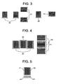
- Fig.3 separately shows alignment marks X1 and Y1 (main scale) to be formed in the underlying layer having a circuit pattern and alignment marks X2 and Y2 (auxiliary scale) to be formed in a resist layer formed on the circuit pattern. More specifically, the marks in Fig.3 have a line-and-space pattern. These marks are formed by a plurality of parallel linear segments of which the line width and the line space are similar to those of the circuit pattern. The marks in Fig.3 have a line-and-space pattern. Thus, for a circuit pattern of 0.3 micrometer rule, the mark having a line-and-space pattern of which the line width and the line apace are 0.3 micronmeter is employed. The marks are formed in a marginal area outside the circuit pattern and the resist pattern.
- the amount of misalignment due to lens aberration generated during transfer of a circuit pattern on a reticle to a wafer by a stepper is generally changed depending on the line width and the line space.
- a similar degree of influence due to the lens aberration received by the circuit pattern can be provided to the alignment marks by making the line width and the line space of the alignment marks similar to the line width and the line space of the circuit pattern.
- the amount of the misalignment of the circuit pattern can be accurately measured by using the alignment marks.
- Fig.4 shows an aligned state of the alignment marks X1 and Y1 and the alignment marks X2 and Y2 on the marginal area or a state at a time of measuring an accuracy of alignment between the patterns of the overlying and underlying layers after the formation of the resist pattern of the overlying layer.
- the accuracy of the alignment in the X direction can be measured by detecting the positional relation between the alignment marks X1 and X2, and the accuracy of the alignment in the Y direction can be measured by detecting the positional relation between the marks Y1 and Y2.
- the position measurement is performed by treating an optical wave signal shown in Fig.5.
- the position information in connection with the alignment marks is obtained from the waveform excluding partial waveforms w1 and w2 shown by the hatching and generated at lines 11 and 12 at the both ends from the optical signal waveform generated from the line-and-space pattern.
- the amount of misalignment is changed depending on the line width and the line space. Since the alignment mark is formed as the line-and-space pattern as shown in Fig.3, the amount of the misalignment of the circuit pattern due to the lens aberration of the stepper can be accurately reflected to the alignment mark.
- a main factor for generating the above stepper lens aberration which causes the misalignment of the patterns of which a degree is influenced by the line width and the line space is known to be a frame aberration. Since, however, in the present embodiment, the position measurement is conducted based on the waveform excluding the partial waveforms w1 and w2 generated at both end lines 11 and 12 of the line-and-space pattern, the lines 11 and 12 of which a shape may be changed due to the influence of the frame aberration can be neglected to accurately measure the minute misalignment due to the frame aberration.
- FIG.6 and 7 Another embodiment of a wafer having an alignment mark in which an amount of misalignment of a circuit pattern due to stepper lens aberration can be accurately measured will be described referring to Figs.6 and 7 in which X3, Ys and 23 are alignment marks on an underlying layer and X4, Y4 and 24 are alignment marks on a resist layer.
- the numerals 23 and 24 denote box marks for automatic measurement of misalignment generally employed, and the alignment marks X3 and X4 and the alignment marks X4 and Y4 disposed near the box marks 23 and 24, respectively, denote line-and space patterns having a line width substantially the same as that of the circuit pattern.
- the box mark 23 and 24 generally employed have a size of 10 micrometers or more, an amount of misalignment thereof is much larger than that of a circuit pattern of which a line width is 1 micrometer or less.
- a difference between influences to the misalignment received by the alignment marks 23 and 24 and to that received by the alignment marks X3, Y3,X4 and Y4 can be measured in advance because the alignment marks X3, Y3,X4 and Y4 of the line-and-space patterns are disposed near the box marks 23 and 24.
- the amounts of the misalignment in the X and Y directions of the circuit pattern can be accurately measured by automatically measuring the misalignment of the underlying layer and the resist layer aligned with each other by means of the conventional method employing the alignment marks 23 and 24 together with by measuring a distance 15 between the marks X3 and X4 and a distance 16 between the alignment marks Y3 and Y4 with a scanning electron microscope (SEM) as shown in Fig.7.
- SEM scanning electron microscope
- the difference between the result of the automatic measurement of the misalignment and the amount of the misalignment of the circuit pattern can be calculated from the difference between the result of the automatic measurement of the alignment marks 23 and 24 and measurement result of the distances 15 and 16 with SEM.
- the amounts of the misalignment of the circuit pattern in the X and Y directions can be accurately measured in the following measurement only by the automatic measurement of the alignment marks 23 and 24 followed by simple addition of the difference, as an offset value, between the result of the automatic measurement and the measurement result of the distances 15 and 16.
- the above method is effective when the direct and automatic measurement is difficult because the line-and-space patterns X3, Y3, X4 and Y4 having similar line widths to those of the circuit patterns are minute in sizes.
- the accurate measurement can be performed without changing the marks 23 and 24.
Landscapes
- Physics & Mathematics (AREA)
- General Physics & Mathematics (AREA)
- Exposure Of Semiconductors, Excluding Electron Or Ion Beam Exposure (AREA)
- Exposure And Positioning Against Photoresist Photosensitive Materials (AREA)
Applications Claiming Priority (2)
| Application Number | Priority Date | Filing Date | Title |
|---|---|---|---|
| JP30677798 | 1998-10-28 | ||
| JP10306777A JP2000133576A (ja) | 1998-10-28 | 1998-10-28 | 位置ずれ計測マーク及び位置ずれ計測方法 |
Publications (1)
| Publication Number | Publication Date |
|---|---|
| EP0997782A1 true EP0997782A1 (fr) | 2000-05-03 |
Family
ID=17961151
Family Applications (1)
| Application Number | Title | Priority Date | Filing Date |
|---|---|---|---|
| EP99121509A Withdrawn EP0997782A1 (fr) | 1998-10-28 | 1999-10-28 | Photomasque comprenant des marques de positionnement, méthode pour évaluer le positionnement |
Country Status (3)
| Country | Link |
|---|---|
| EP (1) | EP0997782A1 (fr) |
| JP (1) | JP2000133576A (fr) |
| KR (1) | KR20000029347A (fr) |
Cited By (11)
| Publication number | Priority date | Publication date | Assignee | Title |
|---|---|---|---|---|
| EP1162507A3 (fr) * | 2000-06-08 | 2005-01-05 | Kabushiki Kaisha Toshiba | Méthode d'alignement, méthode d'inspection d'erreurs de recouvrement, et photomasque |
| US6858948B2 (en) | 2001-05-23 | 2005-02-22 | Asml Netherlands B.V. | Substrate provided with an alignment mark in a substantially transmissive process layer, mask for exposing said mark, device manufacturing method, and device manufactured thereby |
| EP1328774A4 (fr) * | 2000-09-01 | 2010-11-17 | Kla Tencor Corp | Amelioration apportee a une marque de mesure d'alignement de recouvrement |
| US7863763B2 (en) | 2005-11-22 | 2011-01-04 | Asml Netherlands B.V. | Binary sinusoidal sub-wavelength gratings as alignment marks |
| CN102385263A (zh) * | 2010-08-25 | 2012-03-21 | 中芯国际集成电路制造(上海)有限公司 | 对前层图形进行对准的方法以及该方法适用的光罩 |
| CN102386322A (zh) * | 2010-08-25 | 2012-03-21 | 中芯国际集成电路制造(上海)有限公司 | 提高对准精度的方法 |
| CN103135826A (zh) * | 2011-11-27 | 2013-06-05 | 宸鸿科技(厦门)有限公司 | 触控感测装置及其制造方法 |
| CN103529659A (zh) * | 2013-10-29 | 2014-01-22 | 天津芯硕精密机械有限公司 | 一种对位精度检测方法及系统 |
| US10324379B2 (en) | 2015-06-23 | 2019-06-18 | Asml Netherlands B.V. | Lithographic apparatus and method |
| CN111198478A (zh) * | 2018-11-20 | 2020-05-26 | 长鑫存储技术有限公司 | 掩膜组件及套准量测方法 |
| CN112631069A (zh) * | 2020-12-22 | 2021-04-09 | 长江存储科技有限责任公司 | 掩膜板和修正套刻精度的方法 |
Families Citing this family (9)
| Publication number | Priority date | Publication date | Assignee | Title |
|---|---|---|---|---|
| JP4528464B2 (ja) * | 2000-06-08 | 2010-08-18 | 株式会社東芝 | アライメント方法、重ね合わせ検査方法及びフォトマスク |
| EP1314198B1 (fr) * | 2000-08-30 | 2017-03-08 | KLA-Tencor Corporation | Repere de superposition, procedes servant a concevoir des reperes de superposition et procedes de mesure de superposition |
| JP4011353B2 (ja) * | 2002-01-31 | 2007-11-21 | 沖電気工業株式会社 | 合わせ測定用のレジストパターン |
| JP2004134473A (ja) * | 2002-10-09 | 2004-04-30 | Nikon Corp | 位置検出用マーク、位置検出装置、位置検出方法、露光装置、および露光方法 |
| SG108975A1 (en) * | 2003-07-11 | 2005-02-28 | Asml Netherlands Bv | Marker structure for alignment or overlay to correct pattern induced displacement, mask pattern for defining such a marker structure and lithographic projection apparatus using such a mask pattern |
| JP2007035768A (ja) * | 2005-07-25 | 2007-02-08 | Toshiba Corp | 合わせずれ検査用マークの形成方法及び半導体装置の製造方法 |
| KR100831249B1 (ko) * | 2007-06-26 | 2008-05-22 | 주식회사 동부하이텍 | 레티클 정렬 방법 |
| JP2024031595A (ja) * | 2022-08-26 | 2024-03-07 | テルモ株式会社 | 取付状態判定方法、取付状態判定システム及びコンピュータプログラム |
| US20240337953A1 (en) * | 2023-04-04 | 2024-10-10 | Kla Corporation | System and method for tracking real-time position for scanning overlay metrology |
Citations (5)
| Publication number | Priority date | Publication date | Assignee | Title |
|---|---|---|---|---|
| EP0370834A2 (fr) * | 1988-11-25 | 1990-05-30 | Nec Corporation | Dispositif semi-conducteur et méthode de fabrication |
| JPH063686A (ja) * | 1992-06-18 | 1994-01-14 | Alps Electric Co Ltd | 液晶表示装置 |
| JPH07120221A (ja) * | 1993-10-26 | 1995-05-12 | Oki Electric Ind Co Ltd | 合成パタンの重ね合わせずれ量検出方法 |
| US5721619A (en) * | 1995-12-18 | 1998-02-24 | Nec Corporation | Misregistration detecting marks for pattern formed on semiconductor substrate |
| US5757507A (en) * | 1995-11-20 | 1998-05-26 | International Business Machines Corporation | Method of measuring bias and edge overlay error for sub-0.5 micron ground rules |
Family Cites Families (5)
| Publication number | Priority date | Publication date | Assignee | Title |
|---|---|---|---|---|
| JP2940553B2 (ja) * | 1988-12-21 | 1999-08-25 | 株式会社ニコン | 露光方法 |
| JPH05109598A (ja) * | 1991-10-18 | 1993-04-30 | Fujitsu Ltd | レチクルの位置合わせ方法 |
| KR970005676B1 (en) * | 1994-01-19 | 1997-04-18 | Hyundai Electronics Ind | Measuring mark of phase shift mask and fabrication method |
| JPH09232202A (ja) * | 1996-02-20 | 1997-09-05 | Mitsubishi Electric Corp | 投影露光装置におけるアライメント方法 |
| JPH10270342A (ja) * | 1997-03-24 | 1998-10-09 | Canon Inc | 半導体製造装置および半導体製造方法 |
-
1998
- 1998-10-28 JP JP10306777A patent/JP2000133576A/ja active Pending
-
1999
- 1999-10-27 KR KR1019990046806A patent/KR20000029347A/ko not_active Ceased
- 1999-10-28 EP EP99121509A patent/EP0997782A1/fr not_active Withdrawn
Patent Citations (5)
| Publication number | Priority date | Publication date | Assignee | Title |
|---|---|---|---|---|
| EP0370834A2 (fr) * | 1988-11-25 | 1990-05-30 | Nec Corporation | Dispositif semi-conducteur et méthode de fabrication |
| JPH063686A (ja) * | 1992-06-18 | 1994-01-14 | Alps Electric Co Ltd | 液晶表示装置 |
| JPH07120221A (ja) * | 1993-10-26 | 1995-05-12 | Oki Electric Ind Co Ltd | 合成パタンの重ね合わせずれ量検出方法 |
| US5757507A (en) * | 1995-11-20 | 1998-05-26 | International Business Machines Corporation | Method of measuring bias and edge overlay error for sub-0.5 micron ground rules |
| US5721619A (en) * | 1995-12-18 | 1998-02-24 | Nec Corporation | Misregistration detecting marks for pattern formed on semiconductor substrate |
Non-Patent Citations (2)
| Title |
|---|
| PATENT ABSTRACTS OF JAPAN vol. 018, no. 194 (P - 1722) 5 April 1994 (1994-04-05) * |
| PATENT ABSTRACTS OF JAPAN vol. 1995, no. 08 29 September 1995 (1995-09-29) * |
Cited By (21)
| Publication number | Priority date | Publication date | Assignee | Title |
|---|---|---|---|---|
| EP1162507A3 (fr) * | 2000-06-08 | 2005-01-05 | Kabushiki Kaisha Toshiba | Méthode d'alignement, méthode d'inspection d'erreurs de recouvrement, et photomasque |
| CN100468623C (zh) * | 2000-06-08 | 2009-03-11 | 株式会社东芝 | 对准方法、套刻检查方法和光掩模 |
| EP1328774A4 (fr) * | 2000-09-01 | 2010-11-17 | Kla Tencor Corp | Amelioration apportee a une marque de mesure d'alignement de recouvrement |
| US6858948B2 (en) | 2001-05-23 | 2005-02-22 | Asml Netherlands B.V. | Substrate provided with an alignment mark in a substantially transmissive process layer, mask for exposing said mark, device manufacturing method, and device manufactured thereby |
| US6876092B2 (en) | 2001-05-23 | 2005-04-05 | Asml Netherlands B.V. | Substrate provided with an alignment mark, method of designing a mask, computer program, mask for exposing said mark, device manufacturing method, and device manufactured thereby |
| US7056805B2 (en) | 2001-05-23 | 2006-06-06 | Asml Netherlands B.V. | Substrate provided with an alignment mark in a substantially transmissive process layer, mask for exposing said mark, device manufacturing method, and device manufactured thereby |
| US7462548B2 (en) | 2001-05-23 | 2008-12-09 | Asml Netherlands B.V. | Substrate provided with an alignment mark in a substantially transmissive process layer, mask for exposing said mark, device manufacturing method, and device manufactured thereby |
| US7560196B2 (en) | 2001-05-23 | 2009-07-14 | Asml Netherlands B.V. | Mask for exposing an alignment mark, and method and computer program for designing the mask |
| US7759029B2 (en) | 2001-05-23 | 2010-07-20 | Asml Netherlands B.V. | Substrate provided with an alignment mark in a substantially transmissive process layer, mask for exposing said mark, device manufacturing method, and device manufactured thereby |
| US7863763B2 (en) | 2005-11-22 | 2011-01-04 | Asml Netherlands B.V. | Binary sinusoidal sub-wavelength gratings as alignment marks |
| CN102385263A (zh) * | 2010-08-25 | 2012-03-21 | 中芯国际集成电路制造(上海)有限公司 | 对前层图形进行对准的方法以及该方法适用的光罩 |
| CN102386322A (zh) * | 2010-08-25 | 2012-03-21 | 中芯国际集成电路制造(上海)有限公司 | 提高对准精度的方法 |
| CN102386322B (zh) * | 2010-08-25 | 2013-07-24 | 中芯国际集成电路制造(上海)有限公司 | 提高对准精度的方法 |
| CN102385263B (zh) * | 2010-08-25 | 2014-10-01 | 中芯国际集成电路制造(上海)有限公司 | 对前层图形进行对准的方法以及该方法适用的光罩 |
| CN103135826A (zh) * | 2011-11-27 | 2013-06-05 | 宸鸿科技(厦门)有限公司 | 触控感测装置及其制造方法 |
| CN103135826B (zh) * | 2011-11-27 | 2015-10-21 | 宸鸿科技(厦门)有限公司 | 触控感测装置及其制造方法 |
| CN103529659A (zh) * | 2013-10-29 | 2014-01-22 | 天津芯硕精密机械有限公司 | 一种对位精度检测方法及系统 |
| US10324379B2 (en) | 2015-06-23 | 2019-06-18 | Asml Netherlands B.V. | Lithographic apparatus and method |
| CN111198478A (zh) * | 2018-11-20 | 2020-05-26 | 长鑫存储技术有限公司 | 掩膜组件及套准量测方法 |
| CN111198478B (zh) * | 2018-11-20 | 2024-02-06 | 长鑫存储技术有限公司 | 掩膜组件及套准量测方法 |
| CN112631069A (zh) * | 2020-12-22 | 2021-04-09 | 长江存储科技有限责任公司 | 掩膜板和修正套刻精度的方法 |
Also Published As
| Publication number | Publication date |
|---|---|
| KR20000029347A (ko) | 2000-05-25 |
| JP2000133576A (ja) | 2000-05-12 |
Similar Documents
| Publication | Publication Date | Title |
|---|---|---|
| EP0997782A1 (fr) | Photomasque comprenant des marques de positionnement, méthode pour évaluer le positionnement | |
| US6137578A (en) | Segmented bar-in-bar target | |
| US6118517A (en) | Mask pattern for alignment | |
| US6128089A (en) | Combined segmented and nonsegmented bar-in-bar targets | |
| US5868560A (en) | Reticle, pattern transferred thereby, and correction method | |
| US7865328B2 (en) | Position detecting method and apparatus | |
| JPH06132189A (ja) | 重ね合わせ精度測定機の測定条件の最適化方法、並びにアラインメントマーク形状あるいは露光装置におけるアラインメントマーク測定方式の最適化方法 | |
| JPH09148243A (ja) | 半導体素子のオーバレイ検査方法 | |
| US5928822A (en) | Method for confirming optimum focus of stepper | |
| JP2859855B2 (ja) | 半導体素子の微細パターンアライメント方法 | |
| JPH07153673A (ja) | 半導体装置の製造方法および測定マークパターン | |
| JP4072465B2 (ja) | 位置検出方法 | |
| US20020048020A1 (en) | Process and apparatus for manufacturing semiconductor device | |
| US7056625B2 (en) | Focus detection structure | |
| KR100392744B1 (ko) | 반도체 장치, 그 제조에 이용하는 포토마스크, 및 그 중첩정밀도 향상 방법 | |
| US6727989B1 (en) | Enhanced overlay measurement marks for overlay alignment and exposure tool condition control | |
| US5928820A (en) | Method for measuring pattern line width during manufacture of a semiconductor device | |
| JP2004134473A (ja) | 位置検出用マーク、位置検出装置、位置検出方法、露光装置、および露光方法 | |
| JP3948084B2 (ja) | 電子線描画用精度測定方法 | |
| US20050244729A1 (en) | Method of measuring the overlay accuracy of a multi-exposure process | |
| CN117434787A (zh) | 设计版图、掩膜版及测量方法 | |
| KR100356757B1 (ko) | 반도체 웨이퍼 패턴의 크기 및 오버레이 측정방법 | |
| US5616438A (en) | Reticle and a method for measuring blind setting accuracy using the same | |
| JPH06324475A (ja) | レチクル | |
| KR20050066889A (ko) | 마스크 정렬 및 오버레이 정렬을 위한 마크 시스템 |
Legal Events
| Date | Code | Title | Description |
|---|---|---|---|
| PUAI | Public reference made under article 153(3) epc to a published international application that has entered the european phase |
Free format text: ORIGINAL CODE: 0009012 |
|
| AK | Designated contracting states |
Kind code of ref document: A1 Designated state(s): DE GB |
|
| AX | Request for extension of the european patent |
Free format text: AL;LT;LV;MK;RO;SI |
|
| 17P | Request for examination filed |
Effective date: 20000814 |
|
| AKX | Designation fees paid |
Free format text: DE GB |
|
| 17Q | First examination report despatched |
Effective date: 20011016 |
|
| 18D | Application deemed to be withdrawn |
Effective date: 20020227 |