EP1004945A2 - Appareil électrophotographique et élément électrophotographique photosensible - Google Patents
Appareil électrophotographique et élément électrophotographique photosensible Download PDFInfo
- Publication number
- EP1004945A2 EP1004945A2 EP99123572A EP99123572A EP1004945A2 EP 1004945 A2 EP1004945 A2 EP 1004945A2 EP 99123572 A EP99123572 A EP 99123572A EP 99123572 A EP99123572 A EP 99123572A EP 1004945 A2 EP1004945 A2 EP 1004945A2
- Authority
- EP
- European Patent Office
- Prior art keywords
- light receiving
- receiving member
- surface layer
- layer
- electrophotographic apparatus
- Prior art date
- Legal status (The legal status is an assumption and is not a legal conclusion. Google has not performed a legal analysis and makes no representation as to the accuracy of the status listed.)
- Granted
Links
Images


Classifications
-
- G—PHYSICS
- G03—PHOTOGRAPHY; CINEMATOGRAPHY; ANALOGOUS TECHNIQUES USING WAVES OTHER THAN OPTICAL WAVES; ELECTROGRAPHY; HOLOGRAPHY
- G03G—ELECTROGRAPHY; ELECTROPHOTOGRAPHY; MAGNETOGRAPHY
- G03G21/00—Arrangements not provided for by groups G03G13/00 - G03G19/00, e.g. cleaning, elimination of residual charge
- G03G21/0005—Arrangements not provided for by groups G03G13/00 - G03G19/00, e.g. cleaning, elimination of residual charge for removing solid developer or debris from the electrographic recording medium
-
- G—PHYSICS
- G03—PHOTOGRAPHY; CINEMATOGRAPHY; ANALOGOUS TECHNIQUES USING WAVES OTHER THAN OPTICAL WAVES; ELECTROGRAPHY; HOLOGRAPHY
- G03G—ELECTROGRAPHY; ELECTROPHOTOGRAPHY; MAGNETOGRAPHY
- G03G5/00—Recording-members for original recording by exposure, e.g. to light, to heat or to electrons; Manufacture thereof; Selection of materials therefor
- G03G5/02—Charge-receiving layers
- G03G5/04—Photoconductive layers; Charge-generation layers or charge-transporting layers; Additives therefor; Binders therefor
- G03G5/08—Photoconductive layers; Charge-generation layers or charge-transporting layers; Additives therefor; Binders therefor characterised by the photoconductive material being inorganic
- G03G5/082—Photoconductive layers; Charge-generation layers or charge-transporting layers; Additives therefor; Binders therefor characterised by the photoconductive material being inorganic and not being incorporated in a bonding material, e.g. vacuum deposited
- G03G5/08214—Silicon-based
- G03G5/08221—Silicon-based comprising one or two silicon based layers
-
- G—PHYSICS
- G03—PHOTOGRAPHY; CINEMATOGRAPHY; ANALOGOUS TECHNIQUES USING WAVES OTHER THAN OPTICAL WAVES; ELECTROGRAPHY; HOLOGRAPHY
- G03G—ELECTROGRAPHY; ELECTROPHOTOGRAPHY; MAGNETOGRAPHY
- G03G5/00—Recording-members for original recording by exposure, e.g. to light, to heat or to electrons; Manufacture thereof; Selection of materials therefor
- G03G5/02—Charge-receiving layers
- G03G5/04—Photoconductive layers; Charge-generation layers or charge-transporting layers; Additives therefor; Binders therefor
- G03G5/08—Photoconductive layers; Charge-generation layers or charge-transporting layers; Additives therefor; Binders therefor characterised by the photoconductive material being inorganic
- G03G5/082—Photoconductive layers; Charge-generation layers or charge-transporting layers; Additives therefor; Binders therefor characterised by the photoconductive material being inorganic and not being incorporated in a bonding material, e.g. vacuum deposited
- G03G5/08214—Silicon-based
- G03G5/08235—Silicon-based comprising three or four silicon-based layers
-
- G—PHYSICS
- G03—PHOTOGRAPHY; CINEMATOGRAPHY; ANALOGOUS TECHNIQUES USING WAVES OTHER THAN OPTICAL WAVES; ELECTROGRAPHY; HOLOGRAPHY
- G03G—ELECTROGRAPHY; ELECTROPHOTOGRAPHY; MAGNETOGRAPHY
- G03G5/00—Recording-members for original recording by exposure, e.g. to light, to heat or to electrons; Manufacture thereof; Selection of materials therefor
- G03G5/02—Charge-receiving layers
- G03G5/04—Photoconductive layers; Charge-generation layers or charge-transporting layers; Additives therefor; Binders therefor
- G03G5/08—Photoconductive layers; Charge-generation layers or charge-transporting layers; Additives therefor; Binders therefor characterised by the photoconductive material being inorganic
- G03G5/082—Photoconductive layers; Charge-generation layers or charge-transporting layers; Additives therefor; Binders therefor characterised by the photoconductive material being inorganic and not being incorporated in a bonding material, e.g. vacuum deposited
- G03G5/08285—Carbon-based
-
- G—PHYSICS
- G03—PHOTOGRAPHY; CINEMATOGRAPHY; ANALOGOUS TECHNIQUES USING WAVES OTHER THAN OPTICAL WAVES; ELECTROGRAPHY; HOLOGRAPHY
- G03G—ELECTROGRAPHY; ELECTROPHOTOGRAPHY; MAGNETOGRAPHY
- G03G5/00—Recording-members for original recording by exposure, e.g. to light, to heat or to electrons; Manufacture thereof; Selection of materials therefor
- G03G5/14—Inert intermediate or cover layers for charge-receiving layers
- G03G5/147—Cover layers
- G03G5/14704—Cover layers comprising inorganic material
Definitions
- the present invention relates to an electrophotographic apparatus, and more particularly to an electrophotographic apparatus with an improved light receiving member.
- a cleaning blade used as a means for removing the residual developer, is put in contact with the surface of the light receiving member to scrape the residual developer therefrom and discharge the untransferred developer to the outside of the system.
- 60-12554 (U.S. Pat. No. 4,559,289) discloses a surface layer containing carbon and halogen atoms in the surface of a photoconductive layer comprised of amorphous silicon containing silicon atoms
- Japanese Patent Application Laid-Open No. 2-111962 discloses a photosensitive member having a surface protecting-lubricating layer provided on an a-Si:H or a-C:H photosensitive layer.
- these publications include no description concerning the relationship between the electrophotographic process and the scraping property of the surface layer.
- the methods for forming the silicon base non-monocrystalline deposited films there are many known methods, including the sputtering method, the method of decomposing a source gas by heat (thermal CVD method), the method of decomposing a source gas by light (photo CVD method), the method of decomposing a source gas by plasma (plasma CVD method), and so on.
- the plasma CVD method which is a method of decomposing a source gas by a glow discharge or the like generated by direct current, high frequency (RF or VHF), or microwave to form a deposited film on a desired substrate such as glass, quartz, a heat-resistant synthetic resin film, stainless steel, or aluminum are now under way to practical use, including not only the method of forming the amorphous silicon deposited films for electrophotography, but also methods for forming deposited films for the other uses, and there are also proposed various apparatuses for such methods.
- RF or VHF high frequency
- the grain diameters of the developer are being decreased and there are frequently used those developers having the weight average grain diameter of 5 to 8 ⁇ m measured by a coulter counter or the like.
- the corona charger corotron, scorotron
- a wire electrode a metal wire such as a gold plated tungsten wire of 50 to 100 ⁇ m ⁇
- a shield plate as main components. That is, the charging and decharging of the light receiving member using the corona charger is carried out by applying a high voltage (about 4 to 8 kV) to the wire electrode to generate a corona current and allowing the corona current to act on the light receiving member.
- the corona charger is excellent in uniform charging and decharging.
- the corona discharge is accompanied by generation of ozone (O 3 ).
- the ozone oxidizes nitrogen in the air to form nitrogen oxides (NOx). Further, the nitrogen oxides react with water in the air to form nitric acid and other products.
- the products due to the corona discharge such as the nitrogen oxides, nitric acid, etc., adhere to and are deposited on the surface of the light receiving member and peripheral devices. Since the corona discharge products have a strong hygroscopic property, deposition of the corona discharge products on the surface of the light receiving member results in reduction of the resistance of the surface due to moisture absorption of the corona discharge products to substantially decrease the charge retaining capability of the light receiving member throughout or in part of the surface, which may cause the image defect called image smearing (the charge in the surface of the light receiving member leaks in the plane directions to destroy or fail to form an electrostatic latent image pattern).
- image smearing the charge in the surface of the light receiving member leaks in the plane directions to destroy or fail to form an electrostatic latent image pattern.
- the corona discharge products adhering to the internal surface of a shield plate of the corona charger are evaporated and liberated not only during operation of the electrophotographic apparatus but also during quiescent periods of the apparatus, e.g. during the nighttime, and they then adhere to the surface of the light receiving member at a part thereof corresponding to the discharge aperture region of the charger and absorb moisture to decrease the resistance of the surface of the light receiving member.
- the a-Si type light receiving member has a surface hardness extremely higher than those of the other light receiving members. Therefore, the corona discharge product adhering to the surface of the light receiving member can not be removed by the ordinary cleaning step of the light receiving member surface, so that the corona discharge product is likely to remain on the light receiving member surface.
- the electrophotographic apparatuses are sometimes provided with a rotating cylindrical developer-carrying member containing a movable magnet or the like therein.
- a rotating cylindrical developer-carrying member containing a movable magnet or the like therein.
- the method of forming on the carrying member a thin layer of a toner as the developer or a mixture of a toner and a carrier and then electrostatically transferring the toner onto a light receiving member having an electrostatic latent image formed thereon.
- a developer such as a toner containing magnetic particles, i.e., a mixture of a toner and a carrier, or a toner containing magnetite but containing no carrier, or the like is used.
- Reduction of the distance between the rotating cylindrical developer-carrying member and the light receiving member increases the electric field applied thereto to thereby allow the developer to be transferred more easily. This affects a portion at the side opposite the above mentioned portion to increase the distance between the above mentioned members to thereby decrease the electric field applied thereto, whereby the developer can be transferred with difficulty than usual. As a result, there is sometimes caused a problem of partial image density irregularity or the like at the period of rotation of the rotating cylindrical developer-carrying member. In order to obviate such phenomena, there is a need for an electrophotographic apparatus that causes no image smearing even when the light receiving member is not heated.
- fine particles of the developer and additives (strontium titanate, silica, etc.) contained in the developer may be scattered in a corona charger to adhere to a wire electrode of the corona charger (hereinafter referred to as a charger wire), thereby causing discharge irregularities.
- a charger wire a wire electrode of the corona charger
- image defects such as linear blank area portions on the image, scale-like black fogs spreading over the entirety of the image, local black dots (0.1 to 0.3 mm ⁇ ) without periodicity, and so on may be caused.
- abnormal discharge may be induced between the contaminated portion of the wire and the light receiving member, thus damaging the surface of the photosensitive member to cause white dot like image defects.
- the measures including a method of increasing the urging pressure of the cleaning blade, a method of increasing the hardness of the elastic rubber blade to increase the rubbing force in order to increase the force for scraping off the developer attached to the surface of the light receiving member, and so on.
- Increasing the hardness of the blade changes the property of the blade from a rubber-like state to a glass state and thus makes the material fragile, so as to shorten the lifetime of the blade.
- the above methods tend to increase the frictional force against the surface of the light receiving member, so that there are some cases in which the uneven shaving of the surface layer is rather promoted.
- the apparatus is also desirably designed without provision of the means for directly or indirectly heating the light receiving member.
- Another object of the invention is to provide a light receiving member and an electrophotographic apparatus that can maintain high image quality regardless of the service environment.
- a yet another object of the invention is to provide a light receiving member and an electrophotographic apparatus that can prevent occurrence of the problems which are liable to be caused by the size reduction of the developer particles.
- another object of the invention is to provide a light receiving member for use in an electro-photographic apparatus for successively repeating the steps of charging, exposure, developing, transfer, separation, and cleaning and effecting scrape cleaning with a blade, which has a small wear resistance and is free of occurrence of contamination of the charge wire while preventing scattering of the toner and to provide a light receiving member and an electrophotographic apparatus to which the corona discharge products are difficult to adhere and in which even when the corona discharge products adheres to the surface, they can be removed easily, thereby providing a light receiving member and an electrophotographic apparatus that can supply a high quality image free from image smearing for a long term under any service environment.
- an electrophotographic apparatus in which a light receiving member is rotated and the steps of charging, exposure, developing, transfer and cleaning are successively repeated and in which a developer of an average particle diameter of 5 to 8 ⁇ m is applied for developing onto a surface of the light receiving member and transferred from the light receiving member surface to a transfer medium and the light receiving member surface after the transfer of the developer is scrape-cleaned with an elastic rubber blade having the modulus of repulsion elasticity of not less than 10% nor more than 50%, wherein the light receiving member has a surface layer comprised of a non-monocrystalline fluorinated carbon film in which the wear loss after copying steps of 10,000 A4-size transfer sheets is not less than 0.1 ⁇ nor more than 100 ⁇ .
- a light receiving member for an electrophotographic apparatus in which the light receiving member is rotated and the steps of charging, exposure, developing, transfer and cleaning are successively repeated and in which a developer of an average particle diameter of 5 to 8 ⁇ m is applied for developing onto a surface of the light receiving member and transferred from the light receiving member surface to a transfer medium and the light receiving member surface after the transfer of the developer is scrape-cleaned with an elastic rubber blade having the modulus of repulsion elasticity of not less than 10% nor more than 50%, wherein the light receiving member has a surface layer comprised of a non-monocrystalline fluorinated carbon film in which the wear loss after copying steps of 10,000 A4-size transfer sheets is not less than 0.1 ⁇ nor more than 100 ⁇ .
- the inventors have focused attention on the relationship between the electrophotographic process and the wear loss (wear amount) of the surface layer of the light receiving member and attempted to improve the water repellency and the wear property of the surface of the light receiving member in an electrophotographic process.
- the combination of the electro-photographic process of the invention with the light receiving member the surface layer of which is comprised of the non-monocrystalline fluorinated carbon film of the invention allows the surface layer to contain fluorine atoms to be improved in water repellency and to prevent deposition of the corona discharge products thereon, that by adjusting the dynamic hardness of the surface layer within the range of 10 to 500 kgf/mm 2 , optionally providing a rubbing means for rubbing the light receiving member surface in any step of the electrophotographic process, and further adjusting the wear loss of the light receiving member surface after copying steps of 10,000 sheets under the given conditions to be not less than 0.1 ⁇ nor more than 100 ⁇ , it is possible to anytime attain a fluorine atom-containing-
- the light receiving member has a surface layer comprised of a non-monocrystalline fluorinated carbon film in which the wear loss after copying steps of 10,000 A4-size transfer sheets is not less than 0.1 ⁇ nor more than 100 ⁇ , the above mentioned excellent results are able to be achieved.
- modulus of repulsion elasticity refers to cushioning properties of an elastic member.
- the modulus of repulsion elasticity is determined by the modulus of repulsion elasticity test based on JIS (Japanese Industrial Standard) K 6301. Specifically, a test piece of an elastic member is held on a support of a modulus of repulsion elasticity testing machine such that a surface of the test piece is in the vertical direction. Then, a horizontally suspended round bar is allowed to fall freely from a predetermined height to collide perpendicularly with the surface of the test piece to thereby rebound.
- the modulus of repulsion elasticity is defined as the percentage of the rebound height of the horizontally suspended round bar relative to the predetermined height (i.e., the falling height of the bar).
- the modulus of repulsion elasticity of the cleaning blade used for the electrophotographic apparatus is smaller than 10%, the nature of the blade changes from a rubber-like state to a glass state, so that the material becomes fragile and tends to decrease the lifetime of the blade.
- the modulus of repulsion elasticity of the cleaning blade is over 50%, there sometimes arise problems of occurrence of chattering of the blade resulting in lowering of the cleaning properties, rolling of the blade resulting in damage of the surface of the light receiving member, and so on.
- the modulus of repulsion elasticity of the cleaning blade is not less than 10% and not more than 50%.
- urethane rubber silicone rubber, butadiene rubber, isoprene rubber, nitrile rubber, natural rubber, and so on and particularly preferred materials are urethane rubber and silicone rubber which are generally used widely for electrophotographic apparatuses in terms of the hardness and ease to process.
- the blade for improving the cleaning property, may be shaped into any form without any limitation as the occasion demands, for example, to a grooved blade as described in Japanese Patent Application Laid-Open No. 54-143149, a projection-added blade as described in Japanese Patent Application Laid-Open No. 57-124777, and so on.
- the publications neither describe nor suggest the relationship between the electrophotographic apparatus using the developing agent of small grain diameters and not provided with the heating means for the light receiving member, and the wear loss of the surface of the light receiving member having the surface layer of amorphous fluorinated carbon film.
- a magnet roller When the rubbing means is provided in the cleaner, a magnet roller, an elastic rubber roller, or the like is employed.
- the materials for the elastic rubber roller there are generally used urethane rubber, silicone rubber, butadiene rubber, isoprene rubber, nitrile rubber, natural rubber, and so on.
- the shape of the roller may include a sponge roller of an expanded material with large pores.
- the rubbing means is in the form of a charging roller which functions as the primary charger and also as the transfer charger
- the materials generally used for the roller include urethane rubber, silicone rubber, butadiene rubber, isoprene rubber, nitrile rubber, natural rubber, and so on.
- the wear loss after the copying steps on 10,000 A4-size transfer sheets (hereinafter, simply referred to as "10,000 sheets wear loss”) is within the range of not less than 0.1 ⁇ nor more than 100 ⁇ , the chatter of the blade due to friction rarely occurs and partial stress in the blade surface and degradation of the rubbing roller are suppressed, thereby relieving local retention of the developer.
- the wear loss is determined on the basis that the transfer of the A-4 size transfer sheet with regard to the light receiving member is carried out in the direction parallel to the short edge side of the sheet with the long edge side of the sheet being parallel to the longitudinal direction of the light receiving member.
- the 10,000 sheets wear loss of the surface layer of the light receiving member used in the present invention is larger than 100 ⁇ , the mechanical strength could be degraded in certain cases. If the wear loss is smaller than 0.1 ⁇ , the surface layer would become resistant to wearing to reduce the effect of scraping the corona discharge products, thereby causing the image smearing in certain cases.
- the optimum thickness of the surface layer used in the light receiving member of the present invention can be determined from the relationship between the wear loss of the surface layer and the lifetime of the electrophotographic apparatus, and it is generally in the range of 0.01 ⁇ m to 10 ⁇ m and preferably in the range of 0.1 ⁇ m to 1 ⁇ m. If the thickness of the surface layer is less than 0.01 ⁇ m, the mechanical strength could be degraded in certain cases. If the thickness is larger than 10 ⁇ m, the residual potential could become high in certain cases.
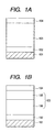
- the a-Si base light receiving member illustrated in Fig. 1B is the light receiving member of the function-separated type in which the photoconductive layer 103 is comprised of a charge transport layer 106 made of an amorphous material containing at least silicon atoms and carbon atoms and a charge generating layer 105 made of an amorphous material containing at least silicon atoms, stacked in series.
- this light receiving member is irradiated with light, carriers generated mainly in the charge generating layer 105 are transported through the charge transport layer 105 to reach the conductive substrate 101.
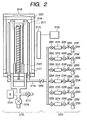
- Fig. 2 is a view schematically showing an example of a deposition apparatus preferably applicable to the production of for the light receiving member by the plasma CVD method (PCVD method).
- PCVD method plasma CVD method
- Described below is an example of procedures in a forming method of the light receiving member, using the apparatus of Fig. 2.
- the main valve 2118 is next opened to evacuate the reaction vessel 2110 and gas supply pipe 2116.
- the high-frequency power source 2120 is set to a desired power and the high-frequency power, for example, of the frequency in the range of 1 MHz to 450 MHz is supplied via the high-frequency matching box 2115 to the cathode electrode 2111 to induce a high-frequency glow discharge.
- This discharge energy decomposes each source gas introduced into the reaction vessel 2110, whereby the desired photoconductive layer with the matrix of silicon atoms is deposited on the cylindrical film-forming substrate 2112.
- the supply of the high-frequency power is stopped and each outflow valve 2251 to 2256 is closed to stop the inflow of each source gas into the reaction vessel 2110, thereby completing the formation of the photoconductive layer.
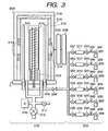
- the material for the cathode electrode 3111 to which the high-frequency power is applied there can be employed copper, aluminum, gold, silver, platinum, lead, nickel, cobalt, iron, chromium, molybdenum, titanium, stainless steel, composite materials of two or more of these materials, and so on.
- the shape of the cathode electrode is preferably a cylindrical shape, but it may be elliptic or polygonal as occasion may demand.
- the cathode electrode 3111 may be provided with a cooling means if necessary.
- a cooling means water, air, liquid nitrogen, a Peltier element, or the like is used as occasion may demand.
- the surface layer of the present invention can also be formed basically by repeating the above operation. Specifically, necessary valves out of the outflow valves 3251 to 3256 and the auxiliary valve 3260 are gradually opened to introduce source gases necessary for the surface layer from the corresponding gas cylinders 3221 to 3226 through the gas inlet pipes 3114 into the reaction vessel 3110. Then each source gas is adjusted to a predetermined flow rate by the corresponding mass flow controller 3211 to 3216. On that occasion, the aperture of the main valve 3118 is adjusted with observing the vacuum gage 3119 so that the pressure inside the reaction vessel 3110 becomes the predetermined pressure of not more than 133 Pa.
- the cylindrical film-forming substrate 3112 may be rotated at a predetermined speed by a driving device (not illustrated) during the period of film formation.
- Fig. 4 is a schematic view showing an example of the structure of the electrophotographic apparatus for explaining an example of an image forming process of the electrophotographic apparatus, in which the light receiving member 401 is arranged to be capable of being temperature-controlled by a surface heater 423 provided inside thereof and to be rotated in the direction of arrow X as occasion may demand.
- a primary charger 402 an electrostatic latent image forming portion 403, a developing device 404, a transfer medium supplying system 405, a transfer charger 406, a separation charger 40, a cleaner 425, a conveying system 408, a charge-eliminating light source 409, and so on as occasion may demand.
- a primary charger 402 an electrostatic latent image forming portion 403
- a developing device 404 Around the light receiving member 401 there are provided a primary charger 402, an electrostatic latent image forming portion 403, a developing device 404, a transfer medium supplying system 405, a transfer charger 406, a separation charger 40, a cleaner 425,
- the light receiving member 401 is uniformly charged by the primary charger 402 to which the high voltage of +6-8 kV is applied.
- a light emitted from a lamp 410 is projected onto an original 412 placed on an original plate 411, the reflected light is guided via mirrors 413, 414, 415 to be focused by lenses 418 of a lens unit 417, the light is guided via a mirror 416 to be projected as an information carrying light onto an electrostatic latent image portion to form an electrostatic latent image on the light receiving member 401.
- a developer of the negative polarity is supplied from the developing device 404 onto the latent image to form a developer image.
- this exposure may also be carried out by scanning exposure with the information carrying light, using an LED array, a laser beam, or a liquid crystal shutter or the like, instead of the reflection from the original 412.
- Fig. 5 is a schematic view showing another example of the electrophotographic apparatus.
- the electrophotographic apparatus shown in Fig. 5 is different from the apparatus of Fig. 4 in that the cleaner 425 as the cleaning means has not only the cleaning blade 421 but also the cleaning roller 426.
- the cleaning step in the electrophotographic apparatus of fig. 5 is carried out as follows.
- the developer remaining on the light receiving member 401 is recovered by a magnetic roller 426 or a cleaning roller 426 made of an elastic material such as silicone rubber, urethane rubber, etc. and a cleaning blade 421 made of an elastic material such as silicone rubber, urethane rubber, etc. provided in the cleaner 425, and the electrostatic latent image remaining thereon is erased by the charge-eliminating light source 409 similarly as above.
- the fluorine content F/(C + F) was measured by the ESCA analysis and the dynamic hardness was then measured using a dynamic ultrafine hardness meter (trade name: DUH-201, mfd. by Shimadzu Corp.).
- the dynamic hardness was represented by the value obtained when an indenter of a triangular pyramid having a radius of curvature of tip of not more than 0.1 ⁇ m and an edge-to-edge angle of 115° was used and the indenter was forced into the sample until a 0.1 gf load was attained.
- the temperature of the surface of the light receiving member was controlled to 60°C to obtain the condition under which the fusion became easier to occur.
- the wear losses of the surface layers after the durability test are also shown in Table 3. The wear losses of the surface layers were obtained by measuring the thicknesses of the surface layers before and after the durability test by a reflection spectroscopic interferometer and calculating the wear losses per 10,000 sheets from these values.
- the elastic rubber blade 421 used was an urethane rubber blade having the modulus of repulsion elasticity of 10% and the cleaning conditions were so set as to effect such scrape cleaning that the urging pressure of the blade was 80% of the ordinary pressure.
- the charging current of the primary charger 402 is adjusted so that the dark area potential is 400 V at the position of the developing device 404.
- An original 412 having vertical lines of solid black is placed on the original plate 411.
- the durability test is conducted by having some portions always rubbed with the developer and the other portions always not rubbed therewith in the direction of the generating line of the surface of the light receiving member.
- the charging current of the primary charger 402 is adjusted so that the dark area potential is 400 V at the position of the developing device 404.
- a solid white original 412 is placed on the original plate 411.
- the on voltage of the halogen lamp 410 is adjusted so that the light area potential is 50 V.
- an original 412 with the reflection density of 0.3 is placed and potential irregularities are measured at this time.
- the potential irregularities are evaluated by percentage of change of a potential of an unevenly scraped portion to a potential of a normal portion.
- the charging current of the primary charger 402 is adjusted so that the dark area potential is 400 V at the position of the developing device 404.
- the original 412 with the reflection density of 0.3 is placed on the original table 411.
- the on voltage of the halogen lamp 410 is adjusted so that the light area potential is 200 V, and a halftone image of A3 size is made. This image is used to observe whether a cleaning failure occurs in a linear pattern.
- the light receiving members 1A, 1B, and 1C had neither the image defect of the black line pattern caused by uneven scraping even after the durability test of 100,000 sheets nor the image defects due to the cleaning failure, the fusion, and the like at all. Further, good image characteristics were also achieved as to the image smearing without provision of the heating means for the light receiving member.
- each of these light receiving members 1A' to 1C' was mounted in the modified machine from the copying machine NP-6085 manufacture by CANON K. K., and the durability test was conducted under the conditions similar to those in Example 1.
- the moving speed of the light receiving member was 300 mm/sec and the blade 421 used was an urethane rubber blade having the modulus of repulsion elasticity of 8%.
- the wear losses of the surface layers after this durability test are shown in Table 7.
- the light receiving members of 1D to 1F were evaluated as to the image smearing by carrying out the durability test of 100,000 sheets under the environment of 35°C and relative humidity 90% without provision of the heating means.
- the cleaning conditions were so set as to effect such scrape cleaning that the urging pressure of the blade was 80% of the ordinary pressure.
- a-C:F surface layer samples of 1D' to 1F' were each prepared on the 7059 glass substrate under the conditions of Table 12, and the fluorine contents and dynamic hardness of the surface layers of 1D' to 1F' were measured by the similar method to that in Example 1.
- the light receiving members 1G', 1H', 1I' were produced by stacking the lower inhibiting layer, charge transport layer and charge generating layer on the cylindrical conductive substrate under the conditions of Table 14 and thereafter depositing the surface layer in a thickness of 0.5 ⁇ m under the conditions of Table 19.
- a-C:F surface layer samples of 1G' to 1I' were each prepared on the 7059 glass substrate under the conditions of Table 19, and the fluorine contents and dynamic hardness of the surface layers of 1G' to 1I' were measured by the similar method to that in Example 1.
- edge portion of the urethane rubber blade after the durability test was observed by a metallurgical microscope with the result that any break such as flaw or the like was not recognized and the initial state was maintained.
- a-C:F surface layer samples of 2D' to 2F' were each prepared on the 7059 glass substrate under the conditions of Table 38, and the fluorine contents and dynamic hardness of the surface layers of 2D' to 2F' were measured by the similar method to that in Example 5.
- the fluorine contents and dynamic hardness of the surface layers of the light receiving members 2D' to 2F' were the values shown in Table 39.
- edge portion of the urethane rubber blade after the durability test was observed by a metallurgical microscope with the result that breaks such as flaw or the like were recognized.
- the light receiving members 2J, 2K, 2L were produced by stacking the lower inhibiting layer, charge transport layer and charge generating layer on the cylindrical conductive substrate under the conditions of Table 40 and thereafter depositing the surface layer in a thickness of 0.5 ⁇ m under the conditions of Table 49.
- the electrophotographic apparatus having the structure for scrape-cleaning the developer of the average particle diameter of 5 to 8 ⁇ m with the elastic rubber blade having the modulus of repulsion elasticity of not less than 10% nor more than 50%
- the light receiving member having the surface layer comprised of the non-monocrystalline fluorinated carbon film in which the wear loss after copying steps of 10,000 A4-size transfer sheets was not less than 0.1 ⁇ nor more than 100 ⁇ , in which the fluorine content was not less than 5 atomic % nor more than 50 atomic %, and in which the dynamic hardness is within the range of 10 to 500 kgf/mm 2 , it has become possible to allow the surface layer to uniformly wear and also to prevent the image density irregularities caused by the uneven scraping and the fusion of the developer.
- the present invention has enabled to remarkably extend the latitude of design of the electrophotographic apparatus, including the types of developers that can be used, size reduction of the electrophotographic apparatus, reduction of cost, and so on.
Landscapes
- Physics & Mathematics (AREA)
- General Physics & Mathematics (AREA)
- Chemical & Material Sciences (AREA)
- Inorganic Chemistry (AREA)
- Photoreceptors In Electrophotography (AREA)
- Cleaning In Electrography (AREA)
Applications Claiming Priority (4)
| Application Number | Priority Date | Filing Date | Title |
|---|---|---|---|
| JP33793898A JP2000162800A (ja) | 1998-11-27 | 1998-11-27 | 電子写真装置 |
| JP33794298 | 1998-11-27 | ||
| JP33794298A JP2000162802A (ja) | 1998-11-27 | 1998-11-27 | 電子写真装置 |
| JP33793898 | 1998-11-27 |
Publications (3)
| Publication Number | Publication Date |
|---|---|
| EP1004945A2 true EP1004945A2 (fr) | 2000-05-31 |
| EP1004945A3 EP1004945A3 (fr) | 2001-09-12 |
| EP1004945B1 EP1004945B1 (fr) | 2005-07-27 |
Family
ID=26575955
Family Applications (1)
| Application Number | Title | Priority Date | Filing Date |
|---|---|---|---|
| EP99123572A Expired - Lifetime EP1004945B1 (fr) | 1998-11-27 | 1999-11-26 | Appareil électrophotographique et élément électrophotographique photosensible |
Country Status (3)
| Country | Link |
|---|---|
| US (1) | US6218064B1 (fr) |
| EP (1) | EP1004945B1 (fr) |
| DE (1) | DE69926326T2 (fr) |
Family Cites Families (15)
| Publication number | Priority date | Publication date | Assignee | Title |
|---|---|---|---|---|
| JPS598831B2 (ja) | 1977-09-10 | 1984-02-27 | キヤノン株式会社 | トナ−層形成装置 |
| JPS54143149A (en) | 1978-04-27 | 1979-11-08 | Minolta Camera Co Ltd | Photosensitive element cleaning device for zerographic copier |
| JPS57124777A (en) | 1981-01-27 | 1982-08-03 | Konishiroku Photo Ind Co Ltd | Cleaning device |
| JPS58144865A (ja) | 1982-02-22 | 1983-08-29 | Konishiroku Photo Ind Co Ltd | 現像方法 |
| JPS607451A (ja) | 1983-06-28 | 1985-01-16 | Canon Inc | 現像装置 |
| JPS6012554A (ja) | 1983-07-04 | 1985-01-22 | Fuji Photo Film Co Ltd | 電子写真用感光体 |
| US4675265A (en) * | 1985-03-26 | 1987-06-23 | Fuji Electric Co., Ltd. | Electrophotographic light-sensitive element with amorphous C overlayer |
| US4910111A (en) * | 1985-12-27 | 1990-03-20 | Sharp Kabushiki Kaisha | Electrophotographic photoreceptor comprising amorphous silicon layer coated with amorphous inorganic material |
| JPH01227161A (ja) * | 1988-03-07 | 1989-09-11 | Minolta Camera Co Ltd | 感光体及びその製造方法 |
| JPH02111962A (ja) | 1988-10-21 | 1990-04-24 | Hitachi Ltd | 電子写真感光体 |
| JP3345700B2 (ja) * | 1994-01-11 | 2002-11-18 | 株式会社リコー | 電子写真用感光体 |
| US5900342A (en) * | 1996-04-26 | 1999-05-04 | Eastman Kodak Company | Photoconductive element having an outermost layer of a fluorinated diamond-like carbon and method of making the same |
| JPH1049018A (ja) * | 1996-07-31 | 1998-02-20 | Minolta Co Ltd | 画像形成装置 |
| JPH112912A (ja) * | 1997-04-14 | 1999-01-06 | Canon Inc | 光受容部材、該光受容部材を有する像形成装置及び該光受容部材を用いた像形成方法 |
| US6001521A (en) * | 1997-10-29 | 1999-12-14 | Canon Kabushiki Kaisha | Electrophotographic photosensitive member |
-
1999
- 1999-11-24 US US09/449,678 patent/US6218064B1/en not_active Expired - Fee Related
- 1999-11-26 DE DE69926326T patent/DE69926326T2/de not_active Expired - Fee Related
- 1999-11-26 EP EP99123572A patent/EP1004945B1/fr not_active Expired - Lifetime
Also Published As
| Publication number | Publication date |
|---|---|
| EP1004945A3 (fr) | 2001-09-12 |
| DE69926326D1 (de) | 2005-09-01 |
| US6218064B1 (en) | 2001-04-17 |
| EP1004945B1 (fr) | 2005-07-27 |
| DE69926326T2 (de) | 2006-05-24 |
Similar Documents
| Publication | Publication Date | Title |
|---|---|---|
| US6183930B1 (en) | Electrophotographic photosensitive member having surface of non-monocrystalline carbon with controlled wear loss | |
| JP3530667B2 (ja) | 電子写真感光体およびその製造方法 | |
| JPH1083091A (ja) | 電子写真感光体及びその製造方法 | |
| US5958644A (en) | Process to form light-receiving member with outer layer made by alternately forming and etching | |
| JP2000003055A (ja) | 電子写真装置 | |
| EP0957413B1 (fr) | Procédé de nettoyage utilisé dans un appareil électrophotographique et procédé électrophotographique utlisant ce procédé | |
| JP2002229303A (ja) | 電子写真装置 | |
| EP0962838B1 (fr) | Appareil et méthode de formation d'images | |
| JP2004133397A (ja) | 電子写真感光体 | |
| EP1004945B1 (fr) | Appareil électrophotographique et élément électrophotographique photosensible | |
| JP3710304B2 (ja) | 電子写真装置 | |
| EP1004938A1 (fr) | Elément photosensible électrophotographique et appareil électrophotographique le comprenant | |
| JP2002149029A (ja) | 画像形成方法、画像形成装置、及び感光体 | |
| JP3507406B2 (ja) | 画像形成方法および感光体 | |
| JP2001337474A (ja) | 光受容部材の製造方法、光受容部材、及び電子写真装置 | |
| JP2000162800A (ja) | 電子写真装置 | |
| JP2000162802A (ja) | 電子写真装置 | |
| JP2003280334A (ja) | 画像形成装置 | |
| JP3571917B2 (ja) | 電子写真装置 | |
| JP2001330977A (ja) | 電子写真装置 | |
| JP2000010313A (ja) | 電子写真装置 | |
| JPH11249523A (ja) | 電子写真システム | |
| JP2001290338A (ja) | 電子写真装置 | |
| JPH10177265A (ja) | 光受容部材の製造方法、該方法による光受容部材、該部材を有する電子写真装置、および該部材を用いる電子写真プロセス | |
| JPH11249328A (ja) | 光受容部材 |
Legal Events
| Date | Code | Title | Description |
|---|---|---|---|
| PUAI | Public reference made under article 153(3) epc to a published international application that has entered the european phase |
Free format text: ORIGINAL CODE: 0009012 |
|
| AK | Designated contracting states |
Kind code of ref document: A2 Designated state(s): AT BE CH CY DE DK ES FI FR GB GR IE IT LI LU MC NL PT SE Kind code of ref document: A2 Designated state(s): DE FR GB IT |
|
| AX | Request for extension of the european patent |
Free format text: AL;LT;LV;MK;RO;SI |
|
| PUAL | Search report despatched |
Free format text: ORIGINAL CODE: 0009013 |
|
| AK | Designated contracting states |
Kind code of ref document: A3 Designated state(s): AT BE CH CY DE DK ES FI FR GB GR IE IT LI LU MC NL PT SE |
|
| AX | Request for extension of the european patent |
Free format text: AL;LT;LV;MK;RO;SI |
|
| RIC1 | Information provided on ipc code assigned before grant |
Free format text: 7G 03G 21/00 A, 7G 03G 5/14 B, 7G 03G 5/147 B, 7G 03G 5/082 B |
|
| 17P | Request for examination filed |
Effective date: 20020123 |
|
| 17Q | First examination report despatched |
Effective date: 20020410 |
|
| AKX | Designation fees paid |
Free format text: DE FR GB IT |
|
| GRAP | Despatch of communication of intention to grant a patent |
Free format text: ORIGINAL CODE: EPIDOSNIGR1 |
|
| GRAS | Grant fee paid |
Free format text: ORIGINAL CODE: EPIDOSNIGR3 |
|
| GRAA | (expected) grant |
Free format text: ORIGINAL CODE: 0009210 |
|
| AK | Designated contracting states |
Kind code of ref document: B1 Designated state(s): DE FR GB IT |
|
| REG | Reference to a national code |
Ref country code: GB Ref legal event code: FG4D |
|
| REF | Corresponds to: |
Ref document number: 69926326 Country of ref document: DE Date of ref document: 20050901 Kind code of ref document: P |
|
| ET | Fr: translation filed | ||
| PLBE | No opposition filed within time limit |
Free format text: ORIGINAL CODE: 0009261 |
|
| STAA | Information on the status of an ep patent application or granted ep patent |
Free format text: STATUS: NO OPPOSITION FILED WITHIN TIME LIMIT |
|
| 26N | No opposition filed |
Effective date: 20060428 |
|
| PGFP | Annual fee paid to national office [announced via postgrant information from national office to epo] |
Ref country code: DE Payment date: 20071130 Year of fee payment: 9 |
|
| PGFP | Annual fee paid to national office [announced via postgrant information from national office to epo] |
Ref country code: IT Payment date: 20071120 Year of fee payment: 9 |
|
| PGFP | Annual fee paid to national office [announced via postgrant information from national office to epo] |
Ref country code: GB Payment date: 20071112 Year of fee payment: 9 Ref country code: FR Payment date: 20071122 Year of fee payment: 9 |
|
| GBPC | Gb: european patent ceased through non-payment of renewal fee |
Effective date: 20081126 |
|
| PG25 | Lapsed in a contracting state [announced via postgrant information from national office to epo] |
Ref country code: IT Free format text: LAPSE BECAUSE OF NON-PAYMENT OF DUE FEES Effective date: 20081126 |
|
| REG | Reference to a national code |
Ref country code: FR Ref legal event code: ST Effective date: 20090731 |
|
| PG25 | Lapsed in a contracting state [announced via postgrant information from national office to epo] |
Ref country code: DE Free format text: LAPSE BECAUSE OF NON-PAYMENT OF DUE FEES Effective date: 20090603 |
|
| PG25 | Lapsed in a contracting state [announced via postgrant information from national office to epo] |
Ref country code: GB Free format text: LAPSE BECAUSE OF NON-PAYMENT OF DUE FEES Effective date: 20081126 |
|
| PG25 | Lapsed in a contracting state [announced via postgrant information from national office to epo] |
Ref country code: FR Free format text: LAPSE BECAUSE OF NON-PAYMENT OF DUE FEES Effective date: 20081130 |