EP1005068A2 - GaN film avec des densités de dislocations filetées reduites et son procédé de fabrication - Google Patents
GaN film avec des densités de dislocations filetées reduites et son procédé de fabrication Download PDFInfo
- Publication number
- EP1005068A2 EP1005068A2 EP99402960A EP99402960A EP1005068A2 EP 1005068 A2 EP1005068 A2 EP 1005068A2 EP 99402960 A EP99402960 A EP 99402960A EP 99402960 A EP99402960 A EP 99402960A EP 1005068 A2 EP1005068 A2 EP 1005068A2
- Authority
- EP
- European Patent Office
- Prior art keywords
- semiconductor layer
- underlying
- semiconductor
- thin film
- facets
- Prior art date
- Legal status (The legal status is an assumption and is not a legal conclusion. Google has not performed a legal analysis and makes no representation as to the accuracy of the status listed.)
- Granted
Links
Images


Classifications
-
- C—CHEMISTRY; METALLURGY
- C30—CRYSTAL GROWTH
- C30B—SINGLE-CRYSTAL GROWTH; UNIDIRECTIONAL SOLIDIFICATION OF EUTECTIC MATERIAL OR UNIDIRECTIONAL DEMIXING OF EUTECTOID MATERIAL; REFINING BY ZONE-MELTING OF MATERIAL; PRODUCTION OF A HOMOGENEOUS POLYCRYSTALLINE MATERIAL WITH DEFINED STRUCTURE; SINGLE CRYSTALS OR HOMOGENEOUS POLYCRYSTALLINE MATERIAL WITH DEFINED STRUCTURE; AFTER-TREATMENT OF SINGLE CRYSTALS OR A HOMOGENEOUS POLYCRYSTALLINE MATERIAL WITH DEFINED STRUCTURE; APPARATUS THEREFOR
- C30B25/00—Single-crystal growth by chemical reaction of reactive gases, e.g. chemical vapour-deposition growth
- C30B25/02—Epitaxial-layer growth
-
- H—ELECTRICITY
- H01—ELECTRIC ELEMENTS
- H01S—DEVICES USING THE PROCESS OF LIGHT AMPLIFICATION BY STIMULATED EMISSION OF RADIATION [LASER] TO AMPLIFY OR GENERATE LIGHT; DEVICES USING STIMULATED EMISSION OF ELECTROMAGNETIC RADIATION IN WAVE RANGES OTHER THAN OPTICAL
- H01S5/00—Semiconductor lasers
- H01S5/30—Structure or shape of the active region; Materials used for the active region
-
- B—PERFORMING OPERATIONS; TRANSPORTING
- B29—WORKING OF PLASTICS; WORKING OF SUBSTANCES IN A PLASTIC STATE IN GENERAL
- B29C—SHAPING OR JOINING OF PLASTICS; SHAPING OF MATERIAL IN A PLASTIC STATE, NOT OTHERWISE PROVIDED FOR; AFTER-TREATMENT OF THE SHAPED PRODUCTS, e.g. REPAIRING
- B29C43/00—Compression moulding, i.e. applying external pressure to flow the moulding material; Apparatus therefor
- B29C43/22—Compression moulding, i.e. applying external pressure to flow the moulding material; Apparatus therefor of articles of indefinite length
- B29C43/222—Compression moulding, i.e. applying external pressure to flow the moulding material; Apparatus therefor of articles of indefinite length characterised by the shape of the surface
-
- B—PERFORMING OPERATIONS; TRANSPORTING
- B29—WORKING OF PLASTICS; WORKING OF SUBSTANCES IN A PLASTIC STATE IN GENERAL
- B29C—SHAPING OR JOINING OF PLASTICS; SHAPING OF MATERIAL IN A PLASTIC STATE, NOT OTHERWISE PROVIDED FOR; AFTER-TREATMENT OF THE SHAPED PRODUCTS, e.g. REPAIRING
- B29C43/00—Compression moulding, i.e. applying external pressure to flow the moulding material; Apparatus therefor
- B29C43/22—Compression moulding, i.e. applying external pressure to flow the moulding material; Apparatus therefor of articles of indefinite length
- B29C43/28—Compression moulding, i.e. applying external pressure to flow the moulding material; Apparatus therefor of articles of indefinite length incorporating preformed parts or layers, e.g. compression moulding around inserts or for coating articles
-
- B—PERFORMING OPERATIONS; TRANSPORTING
- B32—LAYERED PRODUCTS
- B32B—LAYERED PRODUCTS, i.e. PRODUCTS BUILT-UP OF STRATA OF FLAT OR NON-FLAT, e.g. CELLULAR OR HONEYCOMB, FORM
- B32B38/00—Ancillary operations in connection with laminating processes
- B32B38/06—Embossing
-
- C—CHEMISTRY; METALLURGY
- C30—CRYSTAL GROWTH
- C30B—SINGLE-CRYSTAL GROWTH; UNIDIRECTIONAL SOLIDIFICATION OF EUTECTIC MATERIAL OR UNIDIRECTIONAL DEMIXING OF EUTECTOID MATERIAL; REFINING BY ZONE-MELTING OF MATERIAL; PRODUCTION OF A HOMOGENEOUS POLYCRYSTALLINE MATERIAL WITH DEFINED STRUCTURE; SINGLE CRYSTALS OR HOMOGENEOUS POLYCRYSTALLINE MATERIAL WITH DEFINED STRUCTURE; AFTER-TREATMENT OF SINGLE CRYSTALS OR A HOMOGENEOUS POLYCRYSTALLINE MATERIAL WITH DEFINED STRUCTURE; APPARATUS THEREFOR
- C30B25/00—Single-crystal growth by chemical reaction of reactive gases, e.g. chemical vapour-deposition growth
- C30B25/02—Epitaxial-layer growth
- C30B25/18—Epitaxial-layer growth characterised by the substrate
-
- C—CHEMISTRY; METALLURGY
- C30—CRYSTAL GROWTH
- C30B—SINGLE-CRYSTAL GROWTH; UNIDIRECTIONAL SOLIDIFICATION OF EUTECTIC MATERIAL OR UNIDIRECTIONAL DEMIXING OF EUTECTOID MATERIAL; REFINING BY ZONE-MELTING OF MATERIAL; PRODUCTION OF A HOMOGENEOUS POLYCRYSTALLINE MATERIAL WITH DEFINED STRUCTURE; SINGLE CRYSTALS OR HOMOGENEOUS POLYCRYSTALLINE MATERIAL WITH DEFINED STRUCTURE; AFTER-TREATMENT OF SINGLE CRYSTALS OR A HOMOGENEOUS POLYCRYSTALLINE MATERIAL WITH DEFINED STRUCTURE; APPARATUS THEREFOR
- C30B29/00—Single crystals or homogeneous polycrystalline material with defined structure characterised by the material or by their shape
- C30B29/10—Inorganic compounds or compositions
- C30B29/40—AIIIBV compounds wherein A is B, Al, Ga, In or Tl and B is N, P, As, Sb or Bi
- C30B29/403—AIII-nitrides
- C30B29/406—Gallium nitride
-
- H—ELECTRICITY
- H10—SEMICONDUCTOR DEVICES; ELECTRIC SOLID-STATE DEVICES NOT OTHERWISE PROVIDED FOR
- H10P—GENERIC PROCESSES OR APPARATUS FOR THE MANUFACTURE OR TREATMENT OF DEVICES COVERED BY CLASS H10
- H10P14/00—Formation of materials, e.g. in the shape of layers or pillars
- H10P14/20—Formation of materials, e.g. in the shape of layers or pillars of semiconductor materials
- H10P14/27—Formation of materials, e.g. in the shape of layers or pillars of semiconductor materials using selective deposition, e.g. simultaneous growth of monocrystalline and non-monocrystalline semiconductor materials
-
- H—ELECTRICITY
- H10—SEMICONDUCTOR DEVICES; ELECTRIC SOLID-STATE DEVICES NOT OTHERWISE PROVIDED FOR
- H10P—GENERIC PROCESSES OR APPARATUS FOR THE MANUFACTURE OR TREATMENT OF DEVICES COVERED BY CLASS H10
- H10P14/00—Formation of materials, e.g. in the shape of layers or pillars
- H10P14/20—Formation of materials, e.g. in the shape of layers or pillars of semiconductor materials
- H10P14/29—Formation of materials, e.g. in the shape of layers or pillars of semiconductor materials characterised by the substrates
- H10P14/2901—Materials
- H10P14/2921—Materials being crystalline insulating materials
-
- H—ELECTRICITY
- H10—SEMICONDUCTOR DEVICES; ELECTRIC SOLID-STATE DEVICES NOT OTHERWISE PROVIDED FOR
- H10P—GENERIC PROCESSES OR APPARATUS FOR THE MANUFACTURE OR TREATMENT OF DEVICES COVERED BY CLASS H10
- H10P14/00—Formation of materials, e.g. in the shape of layers or pillars
- H10P14/20—Formation of materials, e.g. in the shape of layers or pillars of semiconductor materials
- H10P14/29—Formation of materials, e.g. in the shape of layers or pillars of semiconductor materials characterised by the substrates
- H10P14/2924—Structures
- H10P14/2925—Surface structures
-
- H—ELECTRICITY
- H10—SEMICONDUCTOR DEVICES; ELECTRIC SOLID-STATE DEVICES NOT OTHERWISE PROVIDED FOR
- H10P—GENERIC PROCESSES OR APPARATUS FOR THE MANUFACTURE OR TREATMENT OF DEVICES COVERED BY CLASS H10
- H10P14/00—Formation of materials, e.g. in the shape of layers or pillars
- H10P14/20—Formation of materials, e.g. in the shape of layers or pillars of semiconductor materials
- H10P14/32—Formation of materials, e.g. in the shape of layers or pillars of semiconductor materials characterised by intermediate layers between substrates and deposited layers
- H10P14/3202—Materials thereof
- H10P14/3214—Materials thereof being Group IIIA-VA semiconductors
- H10P14/3216—Nitrides
-
- H—ELECTRICITY
- H10—SEMICONDUCTOR DEVICES; ELECTRIC SOLID-STATE DEVICES NOT OTHERWISE PROVIDED FOR
- H10P—GENERIC PROCESSES OR APPARATUS FOR THE MANUFACTURE OR TREATMENT OF DEVICES COVERED BY CLASS H10
- H10P14/00—Formation of materials, e.g. in the shape of layers or pillars
- H10P14/20—Formation of materials, e.g. in the shape of layers or pillars of semiconductor materials
- H10P14/32—Formation of materials, e.g. in the shape of layers or pillars of semiconductor materials characterised by intermediate layers between substrates and deposited layers
- H10P14/3242—Structure
- H10P14/3244—Layer structure
- H10P14/3248—Layer structure consisting of two layers
-
- H—ELECTRICITY
- H10—SEMICONDUCTOR DEVICES; ELECTRIC SOLID-STATE DEVICES NOT OTHERWISE PROVIDED FOR
- H10P—GENERIC PROCESSES OR APPARATUS FOR THE MANUFACTURE OR TREATMENT OF DEVICES COVERED BY CLASS H10
- H10P14/00—Formation of materials, e.g. in the shape of layers or pillars
- H10P14/20—Formation of materials, e.g. in the shape of layers or pillars of semiconductor materials
- H10P14/34—Deposited materials, e.g. layers
- H10P14/3402—Deposited materials, e.g. layers characterised by the chemical composition
- H10P14/3414—Deposited materials, e.g. layers characterised by the chemical composition being group IIIA-VIA materials
- H10P14/3416—Nitrides
-
- B—PERFORMING OPERATIONS; TRANSPORTING
- B29—WORKING OF PLASTICS; WORKING OF SUBSTANCES IN A PLASTIC STATE IN GENERAL
- B29C—SHAPING OR JOINING OF PLASTICS; SHAPING OF MATERIAL IN A PLASTIC STATE, NOT OTHERWISE PROVIDED FOR; AFTER-TREATMENT OF THE SHAPED PRODUCTS, e.g. REPAIRING
- B29C59/00—Surface shaping of articles, e.g. embossing; Apparatus therefor
- B29C59/005—Surface shaping of articles, e.g. embossing; Apparatus therefor characterised by the choice of material
-
- B—PERFORMING OPERATIONS; TRANSPORTING
- B29—WORKING OF PLASTICS; WORKING OF SUBSTANCES IN A PLASTIC STATE IN GENERAL
- B29C—SHAPING OR JOINING OF PLASTICS; SHAPING OF MATERIAL IN A PLASTIC STATE, NOT OTHERWISE PROVIDED FOR; AFTER-TREATMENT OF THE SHAPED PRODUCTS, e.g. REPAIRING
- B29C59/00—Surface shaping of articles, e.g. embossing; Apparatus therefor
- B29C59/02—Surface shaping of articles, e.g. embossing; Apparatus therefor by mechanical means, e.g. pressing
- B29C59/04—Surface shaping of articles, e.g. embossing; Apparatus therefor by mechanical means, e.g. pressing using rollers or endless belts
- B29C59/046—Surface shaping of articles, e.g. embossing; Apparatus therefor by mechanical means, e.g. pressing using rollers or endless belts for layered or coated substantially flat surfaces
-
- B—PERFORMING OPERATIONS; TRANSPORTING
- B32—LAYERED PRODUCTS
- B32B—LAYERED PRODUCTS, i.e. PRODUCTS BUILT-UP OF STRATA OF FLAT OR NON-FLAT, e.g. CELLULAR OR HONEYCOMB, FORM
- B32B2305/00—Condition, form or state of the layers or laminate
- B32B2305/02—Cellular or porous
- B32B2305/022—Foam
-
- B—PERFORMING OPERATIONS; TRANSPORTING
- B32—LAYERED PRODUCTS
- B32B—LAYERED PRODUCTS, i.e. PRODUCTS BUILT-UP OF STRATA OF FLAT OR NON-FLAT, e.g. CELLULAR OR HONEYCOMB, FORM
- B32B2457/00—Electrical equipment
- B32B2457/20—Displays, e.g. liquid crystal displays, plasma displays
-
- B—PERFORMING OPERATIONS; TRANSPORTING
- B32—LAYERED PRODUCTS
- B32B—LAYERED PRODUCTS, i.e. PRODUCTS BUILT-UP OF STRATA OF FLAT OR NON-FLAT, e.g. CELLULAR OR HONEYCOMB, FORM
- B32B37/00—Methods or apparatus for laminating, e.g. by curing or by ultrasonic bonding
- B32B37/14—Methods or apparatus for laminating, e.g. by curing or by ultrasonic bonding characterised by the properties of the layers
- B32B37/15—Methods or apparatus for laminating, e.g. by curing or by ultrasonic bonding characterised by the properties of the layers with at least one layer being manufactured and immediately laminated before reaching its stable state, e.g. in which a layer is extruded and laminated while in semi-molten state
- B32B37/153—Methods or apparatus for laminating, e.g. by curing or by ultrasonic bonding characterised by the properties of the layers with at least one layer being manufactured and immediately laminated before reaching its stable state, e.g. in which a layer is extruded and laminated while in semi-molten state at least one layer is extruded and immediately laminated while in semi-molten state
-
- H—ELECTRICITY
- H10—SEMICONDUCTOR DEVICES; ELECTRIC SOLID-STATE DEVICES NOT OTHERWISE PROVIDED FOR
- H10H—INORGANIC LIGHT-EMITTING SEMICONDUCTOR DEVICES HAVING POTENTIAL BARRIERS
- H10H20/00—Individual inorganic light-emitting semiconductor devices having potential barriers, e.g. light-emitting diodes [LED]
- H10H20/01—Manufacture or treatment
- H10H20/011—Manufacture or treatment of bodies, e.g. forming semiconductor layers
- H10H20/013—Manufacture or treatment of bodies, e.g. forming semiconductor layers having light-emitting regions comprising only Group III-V materials
- H10H20/0133—Manufacture or treatment of bodies, e.g. forming semiconductor layers having light-emitting regions comprising only Group III-V materials with a substrate not being Group III-V materials
- H10H20/01335—Manufacture or treatment of bodies, e.g. forming semiconductor layers having light-emitting regions comprising only Group III-V materials with a substrate not being Group III-V materials the light-emitting regions comprising nitride materials
-
- H—ELECTRICITY
- H10—SEMICONDUCTOR DEVICES; ELECTRIC SOLID-STATE DEVICES NOT OTHERWISE PROVIDED FOR
- H10H—INORGANIC LIGHT-EMITTING SEMICONDUCTOR DEVICES HAVING POTENTIAL BARRIERS
- H10H20/00—Individual inorganic light-emitting semiconductor devices having potential barriers, e.g. light-emitting diodes [LED]
- H10H20/01—Manufacture or treatment
- H10H20/011—Manufacture or treatment of bodies, e.g. forming semiconductor layers
- H10H20/013—Manufacture or treatment of bodies, e.g. forming semiconductor layers having light-emitting regions comprising only Group III-V materials
- H10H20/0137—Manufacture or treatment of bodies, e.g. forming semiconductor layers having light-emitting regions comprising only Group III-V materials the light-emitting regions comprising nitride materials
-
- H—ELECTRICITY
- H10—SEMICONDUCTOR DEVICES; ELECTRIC SOLID-STATE DEVICES NOT OTHERWISE PROVIDED FOR
- H10H—INORGANIC LIGHT-EMITTING SEMICONDUCTOR DEVICES HAVING POTENTIAL BARRIERS
- H10H20/00—Individual inorganic light-emitting semiconductor devices having potential barriers, e.g. light-emitting diodes [LED]
- H10H20/80—Constructional details
- H10H20/81—Bodies
- H10H20/8215—Bodies characterised by crystalline imperfections, e.g. dislocations; characterised by the distribution of dopants, e.g. delta-doping
Definitions
- the present invention relates to a semiconductor thin film made from a compound semiconductor typically composed of a group III nitride, a semiconductor element using the semiconductor thin film, and a semiconductor device using the semiconductor element, and fabrication methods thereof.
- semiconductor light emitting devices such as a semiconductor laser or a light emitting diode (LED), enabling light emission in a range from a visible light region to an ultraviolet light region by using group III nitride based compound semiconductors such as AlGaInN have been actively developed.
- group III nitride based compound semiconductors such as AlGaInN
- a semiconductor laser capable of emitting light in a short-wavelength region has been required to be practically used for improving the recording density of optical disks or the like.
- the above-described semiconductor laser has a problem. As is apparent from a curve showing a change in drive voltage applied to the semiconductor laser with elapsed time, the drive voltage is gradually increased from the initial current-carrying period. This means that the voltage characteristic is gradually degraded with elapsed time.
- the degradation of the voltage characteristic may be dependent on the fact that the group III nitride based compound semiconductor layer formed on the substrate has threading-dislocations (which are defects propagated to pass through the crystal) at a density ranging from about 1 ⁇ 10 8 /cm 2 to about 1 ⁇ 10 9 /cm 2 .
- the density of threading-dislocations in the GaN layer on the SiO 2 mask layer can be reduced to about 1x10 7 /cm 2 .
- an AlGaInN based semiconductor laser diodes formed on the semiconductor layer prepared by adopting the above method can realize the practical life time of 1150 hr or more.
- an active region of the semiconductor element contains the deviation in crystal plane. As a result, various characteristics of the semiconductor element are degraded, and if the semiconductor element is configured as a semiconductor laser, light emission efficiency and life time are reduced.
- a substrate for growth of a GaN based semiconductor which is made from sapphire or SiC as described above, is largely different from the GaN based semiconductor in lattice constant and thermal expansion coefficient, and consequently, if the GaN based semiconductor is directly grown on the substrate, defects such as dislocations occur in the growth layer, with a result that it is difficult to grow a high quality single crystal of the GaN based semiconductor epitaxial layer.
- an underlying GaN layer containing high density threading-dislocations which is formed on the sapphire substrate or SiC substrate via a buffer layer; a mask layer made from SiO 2 and being patterned into stripes arranged with a specific pitch is formed on the underlying GaN layer; and GaN is grown from the underlying GaN layer exposed through openings between the stripes of the mask layer selectively in the lateral direction, to thereby form the GaN semiconductor containing defects at a low density on the mask layer.
- the SiO 2 mask layer is provided for removing threading-dislocations from the substrate side to the semiconductor layer, removal of the mask layer is incompatible with the purpose of reducing the defect density of the semiconductor layer.
- the present inventors have found that while in the lateral growth of a semiconductor, threading-dislocations are bent by growth facets generated accompanied by the growth, such bending of the threading-dislocations can be performed not only by the above growth facets but also by facets artificially formed, and on the basis of the knowledge, the present inventors have accomplished a semiconductor thin film capable of reducing the density of the threading-dislocations at a specific region and also suppressing occurrence of a deviation in crystal orientation, and a semiconductor element using the semiconductor thin film, and a semiconductor device using the semiconductor element, and fabrication methods thereof.
- a semiconductor thin film including an underlying semiconductor layer in which a plurality of facets are arranged, and a selectively grown/buried semiconductor layer formed to cover the underlying semiconductor layer, wherein the facets of the underlying semiconductor layer are formed by planes tiled with respect to the disposition plane of the underlying semiconductor layer.
- a semiconductor element including a semiconductor thin film having an underlying semiconductor layer in which a plurality of facets are arranged and a selectively grown/buried semiconductor layer formed to cover the underlying semiconductor layer, and a semiconductor element main body formed on the semiconductor thin film, that is, on the selectively grown/buried semiconductor layer or on a semiconductor layer formed thereon, wherein the facets are formed by planes tilted with respect to the disposition plane of the underlying semiconductor layer.
- a semiconductor device including: a semiconductor element including a semiconductor thin film and a semiconductor element main body formed on the semiconductor thin film, the semiconductor thin film having an underlying semiconductor layer in which a plurality of facets are arranged and a selectively grown/buried semiconductor layer formed to cover the underlying semiconductor layer; wherein the facets are formed by planes tilted with respect to the disposition plane of the underlying semiconductor layer.
- the semiconductor device of the present invention may be a single semiconductor device using the semiconductor element or a semiconductor integrated circuit system using a plurality of the semiconductor elements.
- a fourth aspect of the present invention there are provided methods of fabricating the above-described semiconductor thin film, semiconductor element and semiconductor device, each method including the steps of forming an underlying semiconductor layer on a substrate in such a manner that a plurality of facets are arranged in the underlying semiconductor layer, and growing a selectively grown/buried semiconductor layer in such a manner that the selectively grown/buried semiconductor layer covers the underlying semiconductor layer, wherein the facets are formed by planes tilted with respect to the disposition plane of the underlying semiconductor layer.
- the facets of the underlying semiconductor layer are artificially formed, and the selectively grown/buried semiconductor layer is epitaxially grown on the underlying semiconductor layer.
- a mask is formed on a plane of the substrate on which the underlying semiconductor layer is to be formed; the underlying semiconductor layer having the facets is formed by selective growth, so-called ELO (Epitaxy Laterally Overgrowth), and the mask is removed; and the selectively grown/buried semiconductor layer is epitaxially grown.
- ELO Epilaxy Laterally Overgrowth
- the selectively growth/buried semiconductor layer is selectively grown from the facets, that is, tilting planes of the underlying semiconductor layer.
- threading-dislocations are formed in the selectively grown/buried semiconductor layer in such a manner that each of the threading-dislocations laterally extends, that is, bendingly extends from one of the facets of the underlying semiconductor layer in the direction substantially along the disposition plane of the underlying semiconductor layer, being joined to another of the threading-dislocations bendingly extending from the opposed one of the facets, and bendingly extends from the joined portion in the direction crossing the disposition plane of the underlying semiconductor layer.
- low defect density regions in which the threading-dislocations are little present can be formed at portions other than the above joined portions of the threading-dislocations in the selectively grown/buried semiconductor layer.
- an active region (operational region) of the semiconductor element is formed on a low defect density region of the selectively grown/buried semiconductor layer or on a semiconductor layer formed thereon, it is possible to enhance the characteristics of the semiconductor element.
- the facet of the present invention means not only a perfect tilting plane but also a plane which is somewhat curved partially or entirely and which has a principal plane tilted at a specific angle ⁇ .
- Fig. 1 is a schematic sectional view of one embodiment of a semiconductor thin film of the present invention.
- the semiconductor thin film has an underlying semiconductor layer 2 in which a plurality of facets 1 are arranged, and a selectively grown/buried semiconductor layer formed to cover the underlying semiconductor layer 2.
- the underlying semiconductor layer 2 is made from a compound semiconductor of a group III nitride type containing gallium (Ga) and nitride (N).
- the selectively grown/buried semiconductor layer is also made from a compound semiconductor of a group III nitride containing Ga and N.
- the facet 1 is formed by a plane tilted with respect to a disposition plane A of the underlying semiconductor layer 2.
- Threading-dislocations "d”, shown by fine lines in Fig. 1, in the selectively grown/buried semiconductor layer 3 are formed in such a manner that each of the threading-dislocations "d” bendingly extends from one of the facets 1 of the underlying semiconductor layer 2 in the direction substantially along the disposition plane of the underlying semiconductor layer 2, being joined to another of the threading-dislocations "d” bendingly extending from the opposed one of the facets 1, and bendingly extends from the joined portion in the direction crossing the disposition plane of the underlying semiconductor layer 2, more specifically, substantially in the vertical direction.
- Fig. 2 is a schematic sectional view of another embodiment of the semiconductor thin film of the present invention.
- a substrate 6 made from C-face sapphire or SiC is first prepared.
- an underlying semiconductor layer 2 in which facets 1 are arranged is formed on one principal plane 6a of the substrate 6 via a buffer layer 7.
- Fig. 3 is a schematic sectional view of a further embodiment of the semiconductor thin film of the present invention.
- a substrate 6 made from C-face sapphire or SiC is first prepared.
- an underlying layer 12 is formed on one principal plane 6a of the substrate 6 via a buffer layer 7, and an underlying semiconductor layer 2 in which facets 1 are arranged is formed on the underlying layer 12.
- Fig. 4 is a schematic sectional view of still a further embodiment of the semiconductor thin film of the present invention.
- a substrate 6 made from a single crystal of a group III nitride is first prepared, and subsequently an underlying semiconductor layer 2 made from a group III nitride in which facets 1 are arranged is directly formed on one principal plane 6a of the substrate 6.
- Figs. 5 to 8 are schematic sectional views of additional embodiments of the semiconductor thin film of the present invention.
- Each of the embodiments shown in Figs. 5 to 8 is configured such that a compound semiconductor layer 8 made from a group III nitride containing nitrogen (N) and at least one kind of group III element selected from a group consisting of gallium (Ga), aluminum (Al), boron (B) and indium (In) is epitaxially grown on the selectively grown/buried semiconductor layer 3 described in the associated one of the embodiments shown in Figs. 1 to 4.
- the threading-dislocations in the underlying selectively grown/buried semiconductor layer 3 extend in the compound semiconductor layer 8, and high defect density regions 4 and low defect density regions 5 with no threading-dislocations are formed in the compound semiconductor layer 8.
- One embodiment of a semiconductor element of the present invention is characterized in that at least an active region, that is, an operational region affected by crystal defects of the semiconductor element is formed in the low defect density region 5 of the selectively grown/buried semiconductor layer of each of the semiconductor thin films shown in Figs. 1 to 4.
- Another embodiment of the semiconductor element of the present invention is characterized in that at least an active region, that is, an operational region affected by crystal defects of the semiconductor element is formed in the low defect density region 5 of the compound semiconductor layer 8 of each of the semiconductor thin films shown in Figs. 5 to 8.
- a deviation in crystal orientation that is, a deviation in c-axis between the underlying semiconductor layer 2 and the selectively grown/buried semiconductor layer 3 or between the underlying semiconductor layer 2 and the compound semiconductor layer 8 expitaxially grown on the selectively grown/buried semiconductor layer 3 is set to be in a range of 0.1° or less.
- a substrate 6 made from a C-face sapphire is prepared, and a buffer layer 7 made from GaN is formed on one principal plane 6a of the C-face sapphire to a thickness of 30 nm by the MOCVD method.
- a substrate temperature is set at 520°C and trimethyl gallium gas ((CH 3 ) 3 Ga)) and ammonia gas (NH 3 ) are used as a source gas.
- An underlying semiconductor layer 2 made from GaN is formed on the buffer layer 7 to a thickness of 2 ⁇ m by the MOCVD method.
- a substrate temperature is set at 1050°C, and the same source gas as that for forming the buffer layer 7 is used.
- threading-dislocations "d”, schematically shown by fine lines in Fig. 9A, are present in the underlying semiconductor layer 2 at a high density of, for example, 1x10 9 /cm 2 .
- a mask 9 is formed on the underlying semiconductor layer 2.
- the mask 9 is formed by forming a dielectric SiO 2 layer over the entire surface of the underlying semiconductor layer 2 at a substrate temperature of 450°C by a CVD method, and patterning the SiO 2 layer by photolithography and etching.
- the SiO 2 layer is coated with a photoresist layer, and the photoresist layer is subjected to exposure and development into a desired pattern having a plurality of stripes spaced at specific intervals.
- the SiO 2 layer is selectively etched using such a patterned photoresist layer as a mask, to form the mask 9 having stripe-shaped openings 9w.
- the stripes extend in the ⁇ 1-100> direction (perpendicular to the paper plane in Fig. 9B) and arranged at the specific intervals in the ⁇ 11-20> direction.
- the resultant substrate in which the mask 9 has been formed on the underlying layer 2 is cleaned by acetone (CH 3 COCH 3 ) and methanol (CH 3 OH), being dipped in diluted hydrochloric acid (HCl) or diluted hydrofluoric acid for 10 sec, and is cleaned by pure water.
- acetone CH 3 COCH 3
- methanol CH 3 OH
- the interiors of the openings 9w of the mask 9 are selectively etched by reactive ion etching (RIE).
- RIE reactive ion etching
- the stripe portions of the mask 9 composed of the SiO 2 layer is somewhat etched, with a result that as shown in Fig. 9C, the width of each opening 9w is widened and simultaneously the underlying semiconductor layer 2 is partially etched, to form grooves 10 each having an approximately V-shaped cross-section.
- the grooves 10 become deeper and wider, so that as shown in Fig. 10A, the mask 9 is removed and the upper ends of the adjacent ones of the grooves 10 are joined to each other.
- stripes 11 each having a triangular cross-section are formed in such a manner as to be arranged in parallel to each other, and facets 1 oppositely tilted at a specific angle are formed on both side of each stripe 11.
- the RIE used for forming the grooves 10 is performed by a parallel plate type RIE system using BCl 3 and N 2 as a source gas under a condition with a power of 15 W and a pressure of 20 mTorr.
- the facets 1 tilted at 45° with respect to the substrate plane, that is, to the underlying semiconductor 2 are formed on both side surfaces of each stripe 11 extending in the ⁇ 1-100> direction.
- the resultant substrate 6 on which respective semiconductor layers have been stacked is sufficiently dipped in hydrofluoric acid (HF) to remove the SiO 2 film remaining on the surface, and is then cleaned by pure water.
- HF hydrofluoric acid
- GaN is epitaxially grown by the MOCVD method.
- GaN is selectively grown from the facets 1 in the lateral direction or in the ⁇ 11-20> direction, that is, in the lateral direction along the disposition plane of the underlying semiconductor layer 2.
- the portions of GaN grown from the opposed facets 1 collide into each other, to bury the grooves 10, and by further continuing the selective growth, GaN is grown in the direction crossing the disposition plane of the underlying semiconductor layer 2, more specifically, substantially in the vertical direction with respect to the disposition plane of the underlying semiconductor layer 2.
- a selectively grown/buried semiconductor layer 3 made from GaN and having a flat surface is formed to entirely cover the underlying semiconductor layer 2.
- a substrate temperature is set at 1050° C, and ammonia gas and trimethyl gallium gas are used as a source gas.
- ammonia gas is allowed to flow at a flow rate being as slightly large as typically 10 l/min and trimethyl gallium gas is fed at such a flow rate that the film growth rate becomes about 4 ⁇ m/hr. Under such a condition, both the gases are allowed to react with each other at atmospheric pressure.
- GaN is grown to perfectly bury the grooves 10, to form the selectively grown/buried semiconductor layer 3 having a flat surface.
- the selectively grown/buried semiconductor layer 3 thus formed was observed by a transmission electron microscope. As a result, it was confirmed that dislocations "d" in the underlying semiconductor layer 2 are bent at the facets 1. Accordingly, at the stage of selective growth of GaN for forming the selectively grown/buried semiconductor layer 3, until the portions of GaN grown from the opposed facets 1 collide with each other, the dislocations "d" passing through the underlying semiconductor layer 2 in the direction substantially perpendicular to the c-axis are bent at the facets 1 which are pseudo-facets artificially formed on the side surfaces of the grooves 10 by etching, and extend not in the vertical direction but in the horizontal direction substantially along the disposition plane of the underlying semiconductor layer 2, that is, along the principal plane of the substrate 6.
- the threading-dislocations "d" extending from the opposed facets 1 are joined to each other and are partially bent, and extend upwardly in the direction crossing the disposition plane of the underlying semiconductor layer 2, that is, in the stacked direction.
- the defect density in the selectively grown/buried semiconductor layer 3 is reduced to 1x10 7 / cm 2 .
- high defect density regions 4 having the threading-dislocations at a high density occur at the joined portions of the threading-dislocations; however, low defect density regions 5 having the dislocations at a low density are formed at the remaining portions.
- a deviation in c-axis between the selectively grown/buried semiconductor layer 3 and the substrate 6 is in a range of 1° or less.
- a semiconductor thin film 40 including the selectively grown/buried semiconductor layer 3 having an extremely high quality can be formed. Accordingly, by providing a semiconductor element or a semiconductor element main body of a semiconductor device on the low defect density regions 5 of the semiconductor thin film 40, it is possible to obtain the semiconductor element or the semiconductor device with an extremely high reliability.
- a substrate 6 made from C-face sapphire is prepared, and a buffer layer 7 made from GaN is formed on a principal plane 6a of the substrate 6 to a thickness of 30 nm by the MOCVD method.
- a substrate temperature is set at 520° C, and trimethyl gallium gas ((CH 3 ) 3 Ga) and ammonia gas (NH 3 ) are used as a source gas.
- An underlying layer 12 made from GaN is flatly formed on the buffer layer 7 to a thickness of 2 ⁇ m by the MOCVD method.
- a substrate temperature is set at 1050° C, and the same source gas as that used for forming the buffer layer 7 is used.
- a mask 13 made from SiO 2 for selective growth of a semiconductor is formed on the flat underlying layer 12 to a thickness of 5 ⁇ m.
- the selective growth mask 13 has a pattern in which stripes extending in the ⁇ 11-20> direction are arranged in parallel to each other with a pitch of 12 ⁇ m (for example, width: 5 ⁇ m, interval: 7 ⁇ m) in the ⁇ 1-100> direction.
- the selective growth mask 13 is formed by forming a SiO 2 layer on the entire surface of the underlying layer 12 at a substrate temperature of 450° C by the CVD method; and patterning the SiO 2 layer by photolithography and pattern etching, that is, coating the SiO 2 layer with a photoresist, patterning the photoresist layer by pattern exposure and development, and selectively etching the SiO 2 layer using the patterned photoresist layer as an etching mask, to form stripe-shaped openings 13w.
- the resultant substrate, on which the selective growth mask 13 has been formed on the underlying layer 12, is cleaned by acetone (CH 3 COCH 3 ) and methanol (CH 3 OH), being dipped in diluted hydrochloric acid (HCl) or diluted hydrofluoric acid (HF) for about 10 sec, and is cleaned by pure water. Further, the substrate is sufficiently dipped in hydrofluoric acid (HF), to perfectly remove SiO 2 remaining on the surface of the underlying layer 12 exposed to the outside through the openings 13w of the selective growth mask 13, and is cleaned by pure water.
- HCl hydrochloric acid
- HF diluted hydrofluoric acid
- a high quality underlying semiconductor layer 2 made from GaN is grown on the underlying layer 12 exposed to the outside through the openings 13w using the selective growth mask 13 as a mask by the MOCVD method until the underlying semiconductor layer 2 covers the mask 13.
- stripes 11 each having a triangular cross-section periodically extend in the ⁇ 11-20> direction and facets 1, each being tilted at about 69° with respect to the C-face of the ⁇ 1-101 ⁇ faces, that is, to the disposition plane of the underlying semiconductor layer 2, are formed on both side surfaces of each stripe 11.
- a substrate temperature is set at 1050° C, and ammonia gas and trimethyl gallium gas are used as a source gas.
- ammonia gas is allowed to flow at a flow rate being as slightly large as typically 10 l/min and trimethyl gallium gas is fed at such a flow rate that the film growth rate becomes about 4 ⁇ m/hr. Under such a condition, both the gases are allowed to react with each other at atmospheric pressure.
- the resultant substrate on which the underlying semiconductor layer 2 has been formed on the underlying layer 12, is sufficiently dipped in hydrofluoric acid (HF) to perfectly remove the selective growth mask 13 by etching. After that, the substrate is cleaned by acetone (CH 3 COCH 3 ) and methanol (CH 3 OH), being dipped in diluted hydrochloric acid (HCl) or diluted hydrofluoric acid (HF) for about 10 sec, and is cleaned by pure water.
- HF hydrofluoric acid
- a selectively grown/buried semiconductor layer 3 made from high quality GaN is selectively grown on the underlying semiconductor layer 2 in which the facets 1 are arranged by the MOCVD method.
- a substrate temperature is set at 1050° C, and ammonia gas and trimethyl gallium gas are used as a source gas.
- ammonia gas is allowed to flow at a flow rate being as slightly large as typically 10 l/min and trimethyl gallium gas is fed at such a flow rate that the film growth rate becomes about 4 ⁇ m/hr. Under such a condition, both the gases are allowed to react with each other at atmospheric pressure.
- GaN is selectively grown from the facets 1 in the lateral direction, that is, in the ⁇ 11-20> direction along the disposition plane of the underlying semiconductor layer 2.
- the portions of GaN grown from the opposed facets 1 collide into each other, to bury grooves 10 between the stripes 11, and by further continuing the selective growth, GaN is grown in the direction perpendicular to the disposition plane of the underlying semiconductor layer 2.
- the selectively grown/buried semiconductor layer 3 made from GaN and having a flat surface is formed to entirely cover the underlying semiconductor layer 2.
- the dislocations "d" extending from the opposed facets 1 are joined to each other and are partially bent, and extend upwardly in the direction crossing the disposition plane of the underlying semiconductor layer 2, that is, in the stacked direction.
- the defect density in the selectively grown/buried semiconductor layer 3 is reduced to 1x10 7 /cm 2 .
- high defect density regions 4 having the threading-dislocations at a high density occur at the joined portions of the threading-dislocations; however, low defect density regions 5 having the dislocations at a low density are formed at the remaining portions.
- a deviation in c-axis between the selectively grown/buried semiconductor layer 3 and the substrate 6 is in a range of 1 ° or less.
- a semiconductor thin film 40 including the selectively grown/buried semiconductor layer 3 having an extremely high quality can be formed. Accordingly, by providing a semiconductor element or a semiconductor element main body of a semiconductor device on the low defect density regions 5 of the semiconductor thin film 40, it is possible to obtain the semiconductor element or the semiconductor device with an extremely high reliability.
- a semiconductor element of the present invention can be fabricated by using the semiconductor thin film 40 in each of the above-described embodiments shown in Figs. 1 to 8.
- Fig. 13 is a schematic sectional view of a semiconductor light emitting element as one embodiment of the semiconductor element of the present invention.
- the semiconductor light emitting element is configured as a SCH (Separate Confinement Heterostructure) type semiconductor laser which has a semiconductor laser element main body formed on the semiconductor thin film 40 shown in Fig. 2 or which is formed as the semiconductor layer 8 of the semiconductor thin film 40 shown in Fig. 6.
- SCH Separatate Confinement Heterostructure
- a first contacting layer 21, a first cladding layer 22, and a first guiding layer 23, each of which is of a first conduction type, for example, n-type, are epitaxially grown in sequence on the selectively grown/buried semiconductor layer 3.
- an active layer 24 and a deterioration preventive layer 25, and further a second guiding layer 26, a second cladding layer 27, and a second contacting layer 28, each of which is of a second conduction type, for example p-type, are sequentially stacked on the first guiding layer 23.
- An insulating layer 29 made from SiO 2 is formed on the second contacting layer 28.
- These layers thus epitaxially grown are partially etched from the insulating layer 29 side until the first contacting layer 21 is exposed, to form an etching groove, and a first electrode 31 is formed in ohmic contact with the exposed portion of the first contacting layer 21.
- a second electrode 32 is formed in ohmic contact with the stripe shaped exposed portion of the second contacting layer 28 through a stripe shaped opening 29w which is formed in the insulating layer 29 in such a manner as to extend in the direction perpendicular to the paper plane in Fig. 13, that is, along the extending direction of the facets 1 or stripe 11 of the semiconductor thin film 40.
- an underlying semiconductor layer 2 in which facets 1 are arranged, and a selectively grown/buried semiconductor layer 3 are formed on a substrate 6 via a buffer layer 7.
- a first contacting layer 21 made from n-type GaN doped with Si and having a thickness of 2 ⁇ m, a first cladding layer 22 made from n-type AlGaN alloy crystal doped with Si and having a thickness of 0.5 ⁇ m, and a first guiding layer 23 made from n-type GaN doped with Si having a thickness of 0.1 ⁇ m are epitaxially grown in sequence on the flat surface of the selectively grown/buried semiconductor layer 3.
- An active layer 24 having a multi-quantum well structure of a quantum well layer having a thickness of 3 nm, a barrier layer having a thickness of 4 nm, and a GaInN alloy crystal layer having a thickness of 4 nm is expitaxially grown on the first guiding layer 23.
- a deterioration preventive layer 25 made from AlGaN and having a thickness of 20 nm is epitaxially grown on the active layer 24.
- a second guiding layer 26 made from p-type GaN doped with a p-type impurity, Mg and having a thickness of 0.1 ⁇ m, a second cladding layer 27 made from p-type AlGaN alloy crystal and having a thickness of 0.5 ⁇ m, and a second contacting layer 28 made from p-type GaN alloy crystal and having a thickness of 0.5 ⁇ m are epitaxially grown in sequence on the deterioration preventive layer 25.
- a substrate temperature is set in a range of 800 to 1000° C; and trimethy aluminum gas ((CH 3 ) 3 Al) is used as a source gas for aluminum, trimethyl gallium gas ((CH 3 ) 3 Ga) is used as a source gas for gallium, ammonia gas (NH 3 ) is used as a source gas for nitrogen, silane gas (SiH 4 ) is used as a source gas for silicon, and bis(methylcyclopentadienyl)magnesium gas (MeCp 2 Mg) or bis(cyclopentadienyl)magnesium gas (Cp 2 Mg) is used as a source gas for magnesium.
- trimethy aluminum gas ((CH 3 ) 3 Al) is used as a source gas for aluminum
- trimethyl gallium gas ((CH 3 ) 3 Ga) is used as a source gas for gallium
- ammonia gas (NH 3 ) is used as a source gas for nitrogen
- silane gas (SiH 4 ) is used as
- the insulating layer 29 is formed by the CVD method, and the stripe shaped opening 29w is formed in the insulating layer 29 by photolithography and pattern etching.
- the second electrode 32 is formed in ohmic contact with the contacting layer 28 through the opening 29w; however, it can be formed by a lift-off method.
- a photoresist layer having a pattern covering a portion other than electrode forming portion is formed by photolithography; Ni and Au are sequentially vapor-deposited over the entire surface; and the patterned resist layer is lifted-off, that is, removed to thereby remove Ni and Au vapor-deposited on the patterned resist layer. In this way, the second electrode 32 made from Ni and Au is formed.
- the insulating layer 29, the contacting layer 28, the second cladding layer 27, the second guiding layer 26, the deterioration preventive layer 25, the active layer 24, the first guiding layer 23, and the first cladding layer 22 are selectively removed in sequence. Then, Ti, Al and Au are selectively vapor-deposited in sequence on the exposed portion of the n-type contacting layer 21, to form a first electrode 31.
- the density of threading-dislocations is extremely low because the density of the threading-dislocations in the selectively grown/buried semiconductor layer 3 is extremely low as described above, and particularly, low defect density regions are formed over the low defect density regions 5 shown in Figs. 2 or 6, and accordingly, in this embodiment, a laser resonator is formed at a position over the low defect density region, that is, substantially over the stripe 11.
- a current injection region is restrictively formed in the active region 24 at a position under the contact portion of the second electrode 32 with the contacting layer 28 through the stripe shaped opening 29w, to form a laser resonator thereat. Accordingly, the opening 29w of the insulating layer 29 equivalent to the contact portion of the second electrode 32 with the contacting layer 28 is formed over the stripe 11.
- the semiconductor element is cut by cleavage to set the length of the laser resonator to a specific value.
- the cut planes form mirror-surfaces constituting end planes of the resonator.
- the semiconductor laser in this embodiment Since at least the operational portion of the semiconductor light emitting element, that is, the semiconductor laser in this embodiment is formed in the region having threading-dislocations at a low density and also occurrence of the deviation in crystal orientation is avoided, it is possible to reduce a threshold current and a drive voltage, and hence to moderate the deterioration of the characteristics caused by the increased threshold current and drive voltage. As a result, the life time of the semiconductor laser in this embodiment can be prolonged.
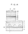
- Fig. 14 is a schematic sectional view of another embodiment of the semiconductor element of the present invention.
- the semiconductor element is configured as a semiconductor laser having the SCH structure which is formed on the semiconductor thin film 40 of the present invention shown in each of Figs. 3 and 7.
- the semiconductor thin film 40 of the semiconductor laser may be fabrication in the same manner as that described with reference to Figs. 11A to 11C and 12A and 12B; and a semiconductor laser main body of the semiconductor laser may be of the same structure as that described with reference to Fig. 13 and the fabrication method thereof may be also the same as that described with reference to Fig. 13.
- the present invention is not limited to the above-described embodiments, and it is to be understood that various variations may be made without departing from the technical thought of the present invention.
- the facets 1 in the case of forming the stripes 11, that is, the facets 1 by selective growth in accordance with the steps shown in Figs. 11A to 11C, by selecting the extending direction of the stripes 11 to the ⁇ 1-100> direction, the facets 1 each being tilted at about 58° with respect to the C-face of the ⁇ 11-22 ⁇ faces, that is, to the disposition plane of the underlying semiconductor layer 2.
- the extending direction of the facets 1, and accordingly, the extending direction of the high defect density regions 4 and the low defect density regions 5 can be selected to any one of directions along various crystal axes.
- the conduction type may be reversed to that described above, and the composition may be different from that described above. That is to say, the present invention can be applied to the semiconductor element in which the above-described semiconductor layers are made from other suitable semiconductors.
- each of the semiconductor layers is made from a compound semiconductor composed of a group III nitride containing nitrogen (N) and at least one kind of group III element selected from a group consisting of Al, Ga, B and In.
- the semiconductor laser in each of the above embodiments has the SCH structure in which the first and second guiding layers 23 and 26 are disposed with the active layer 24 put therebetween
- the present invention can be applied to a semiconductor light emitting element, such as a semiconductor laser or a light emitting diode, which has a different structure such as a DH (Double Hetero) structure with no guiding layers.
- a semiconductor light emitting element such as a semiconductor laser or a light emitting diode, which has a different structure such as a DH (Double Hetero) structure with no guiding layers.
- the semiconductor element of the present invention is not limited to the semiconductor light emitting element but may be another element such as a FET (Field Effect Transistor).
- FET Field Effect Transistor
- a semiconductor device of the present invention can be configured as a single semiconductor device having the above-described semiconductor element or an integrated circuit system in which a plurality of semiconductor elements are formed on a common semiconductor thin film fabricated in accordance with the present invention.
- each of the semiconductor thin films shown in Figs. 1 to 8 may be fabricated in accordance with each of the methods described with reference to Figs. 9A to 12B, and each of the semiconductor elements such as semiconductor light emitting elements having the structures shown in Figs. 13 and 14 may be fabricated in accordance with each of the methods described with reference to Figs. 13 and 14.
- the facets 1 and accordingly the low defect density regions 5 in the common semiconductor thin film 40 may be not necessarily arranged at equal intervals.
- each semiconductor layer may be grown by the MOCVD method or halide vapor-deposition method in the above embodiments, it may be grown by another vapor-deposition method such as a MBE (Molecular Beam Epitaxy) method.
- the semiconductor layers 21 to 28 may be formed by the MBE method or the halide method.
Landscapes
- Chemical & Material Sciences (AREA)
- Engineering & Computer Science (AREA)
- Metallurgy (AREA)
- Organic Chemistry (AREA)
- Crystallography & Structural Chemistry (AREA)
- Materials Engineering (AREA)
- Inorganic Chemistry (AREA)
- General Chemical & Material Sciences (AREA)
- Chemical Kinetics & Catalysis (AREA)
- Mechanical Engineering (AREA)
- Physics & Mathematics (AREA)
- Condensed Matter Physics & Semiconductors (AREA)
- General Physics & Mathematics (AREA)
- Electromagnetism (AREA)
- Optics & Photonics (AREA)
- Led Devices (AREA)
- Semiconductor Lasers (AREA)
- Recrystallisation Techniques (AREA)
Applications Claiming Priority (2)
| Application Number | Priority Date | Filing Date | Title |
|---|---|---|---|
| JP33630798A JP4032538B2 (ja) | 1998-11-26 | 1998-11-26 | 半導体薄膜および半導体素子の製造方法 |
| JP33630798 | 1998-11-26 |
Publications (3)
| Publication Number | Publication Date |
|---|---|
| EP1005068A2 true EP1005068A2 (fr) | 2000-05-31 |
| EP1005068A3 EP1005068A3 (fr) | 2000-11-15 |
| EP1005068B1 EP1005068B1 (fr) | 2004-07-14 |
Family
ID=18297769
Family Applications (1)
| Application Number | Title | Priority Date | Filing Date |
|---|---|---|---|
| EP99402960A Expired - Lifetime EP1005068B1 (fr) | 1998-11-26 | 1999-11-26 | GaN film avec des densités de dislocations filetées reduites et son procédé de fabrication |
Country Status (6)
| Country | Link |
|---|---|
| US (1) | US6576533B2 (fr) |
| EP (1) | EP1005068B1 (fr) |
| JP (1) | JP4032538B2 (fr) |
| KR (1) | KR100700677B1 (fr) |
| DE (1) | DE69918643T2 (fr) |
| TW (1) | TW426989B (fr) |
Cited By (14)
| Publication number | Priority date | Publication date | Assignee | Title |
|---|---|---|---|---|
| WO2002023604A1 (fr) * | 2000-09-18 | 2002-03-21 | Mitsubishi Cable Industries, Ltd. | Materiau de base semi-conducteur et procede de fabrication dudit materiau |
| WO2002103868A1 (fr) * | 2001-06-15 | 2002-12-27 | Sony Corporation | Element laser a semi-conducteurs a faisceaux multiples |
| WO2003025263A1 (fr) * | 2001-09-13 | 2003-03-27 | Japan Science And Technology Agency | Substrat semi-conducteur de nitrure, son procede d'obtention et dispositif optique a semi-conducteur utilisant ledit substrat |
| WO2003034560A1 (fr) * | 2001-10-12 | 2003-04-24 | Sumitomo Electric Industries, Ltd. | Procede pour produire un element electroluminescent semi-conducteur, element electroluminescent semi-conducteur, procede pour produire un element semi-conducteur, element semi-conducteur, procede pour produire un element et element |
| WO2003105295A1 (fr) * | 2002-06-10 | 2003-12-18 | ソニー株式会社 | Laser semi-conducteur a faisceaux multiples, dispositif a semi-conducteur emetteur de rayonnement lumineux et dispositif semi-conducteur |
| FR2842832A1 (fr) * | 2002-07-24 | 2004-01-30 | Lumilog | Procede de realisation par epitaxie en phase vapeur d'un film de nitrure de gallium a faible densite de defaut |
| WO2004061911A3 (fr) * | 2002-12-18 | 2004-09-16 | Agere Systems Inc | Dispositifs a semiconducteur a defauts reduits en zone active et schemas de contact uniques |
| EP1378949A4 (fr) * | 2001-03-21 | 2006-03-22 | Mitsubishi Cable Ind Ltd | Dispositif luminescent semiconducteur |
| CN100440656C (zh) * | 2002-06-20 | 2008-12-03 | 索尼株式会社 | GaN基半导体器件 |
| CN102005523A (zh) * | 2009-09-01 | 2011-04-06 | 夏普株式会社 | 氮化物半导体元件及其制造方法及半导体层的制造方法 |
| US7973377B2 (en) | 2002-12-18 | 2011-07-05 | Infrared Newco, Inc. | Image sensor comprising isolated germanium photodetectors integrated with a silicon substrate and silicon circuitry |
| CN101504962B (zh) * | 2001-03-21 | 2012-10-10 | 三菱化学株式会社 | 半导体发光元件及其制造方法 |
| EP2469581A4 (fr) * | 2009-08-20 | 2013-10-23 | Powdec Kk | Elément semi-conducteur et procédé de production associé |
| US8828579B2 (en) | 2003-04-01 | 2014-09-09 | Sony Corporation | Battery |
Families Citing this family (66)
| Publication number | Priority date | Publication date | Assignee | Title |
|---|---|---|---|---|
| JP4046114B2 (ja) * | 1998-12-21 | 2008-02-13 | 日亜化学工業株式会社 | 窒化物半導体の成長方法及び窒化物半導体素子 |
| JP3427047B2 (ja) * | 1999-09-24 | 2003-07-14 | 三洋電機株式会社 | 窒化物系半導体素子、窒化物系半導体の形成方法および窒化物系半導体素子の製造方法 |
| TW518767B (en) * | 2000-03-31 | 2003-01-21 | Toyoda Gosei Kk | Production method of III nitride compound semiconductor and III nitride compound semiconductor element |
| US6836498B2 (en) * | 2000-06-05 | 2004-12-28 | Sony Corporation | Semiconductor laser, semiconductor device and nitride series III-V group compound substrate, as well as manufacturing method thereof |
| US6627974B2 (en) * | 2000-06-19 | 2003-09-30 | Nichia Corporation | Nitride semiconductor substrate and method for manufacturing the same, and nitride semiconductor device using nitride semiconductor substrate |
| JP4556300B2 (ja) * | 2000-07-18 | 2010-10-06 | ソニー株式会社 | 結晶成長方法 |
| JP3988018B2 (ja) * | 2001-01-18 | 2007-10-10 | ソニー株式会社 | 結晶膜、結晶基板および半導体装置 |
| JP3679720B2 (ja) | 2001-02-27 | 2005-08-03 | 三洋電機株式会社 | 窒化物系半導体素子および窒化物系半導体の形成方法 |
| JP3583375B2 (ja) * | 2001-03-02 | 2004-11-04 | 三菱電線工業株式会社 | GaN系半導体基材およびその製造方法 |
| JP3595276B2 (ja) * | 2001-03-21 | 2004-12-02 | 三菱電線工業株式会社 | 紫外線発光素子 |
| US8633093B2 (en) | 2001-04-12 | 2014-01-21 | Sumitomo Electric Industries Ltd. | Oxygen doping method to gallium nitride single crystal substrate |
| US6773504B2 (en) | 2001-04-12 | 2004-08-10 | Sumitomo Electric Industries, Ltd. | Oxygen doping method to gallium nitride single crystal substrate and oxygen-doped N-type gallium nitride freestanding single crystal substrate |
| JP3714188B2 (ja) | 2001-04-19 | 2005-11-09 | ソニー株式会社 | 窒化物半導体の気相成長方法及び窒化物半導体素子 |
| JP2004262757A (ja) * | 2001-04-24 | 2004-09-24 | Sony Corp | 窒化物半導体、半導体素子およびこれらの製造方法 |
| US7105865B2 (en) | 2001-09-19 | 2006-09-12 | Sumitomo Electric Industries, Ltd. | AlxInyGa1−x−yN mixture crystal substrate |
| JP3864870B2 (ja) * | 2001-09-19 | 2007-01-10 | 住友電気工業株式会社 | 単結晶窒化ガリウム基板およびその成長方法並びにその製造方法 |
| JP4856350B2 (ja) * | 2002-12-16 | 2012-01-18 | Hoya株式会社 | ダイオード |
| JP4201079B2 (ja) * | 2002-12-20 | 2008-12-24 | 昭和電工株式会社 | 発光素子、その製造方法およびledランプ |
| US7462882B2 (en) | 2003-04-24 | 2008-12-09 | Sharp Kabushiki Kaisha | Nitride semiconductor light-emitting device, method of fabricating it, and semiconductor optical apparatus |
| JP2004327655A (ja) * | 2003-04-24 | 2004-11-18 | Sharp Corp | 窒化物半導体レーザ素子、その製造方法および半導体光学装置 |
| US6921924B2 (en) * | 2003-06-18 | 2005-07-26 | United Epitaxy Company, Ltd | Semiconductor light-emitting device |
| JP4593890B2 (ja) * | 2003-07-28 | 2010-12-08 | 京セラ株式会社 | 半導体発光素子の製造方法 |
| JP4540347B2 (ja) * | 2004-01-05 | 2010-09-08 | シャープ株式会社 | 窒化物半導体レーザ素子及び、その製造方法 |
| KR100568300B1 (ko) * | 2004-03-31 | 2006-04-05 | 삼성전기주식회사 | 질화물 반도체 발광소자 및 그 제조방법 |
| JP5013661B2 (ja) * | 2004-03-31 | 2012-08-29 | 三洋電機株式会社 | 窒化物系半導体素子の製造方法及び窒化物系半導体素子 |
| JP3819398B2 (ja) * | 2004-04-27 | 2006-09-06 | 三菱電線工業株式会社 | 半導体発光素子およびその製造方法 |
| US7157297B2 (en) * | 2004-05-10 | 2007-01-02 | Sharp Kabushiki Kaisha | Method for fabrication of semiconductor device |
| JP4651312B2 (ja) * | 2004-06-10 | 2011-03-16 | シャープ株式会社 | 半導体素子の製造方法 |
| JP4720125B2 (ja) * | 2004-08-10 | 2011-07-13 | 日立電線株式会社 | Iii−v族窒化物系半導体基板及びその製造方法並びにiii−v族窒化物系半導体 |
| JP4883931B2 (ja) * | 2005-04-26 | 2012-02-22 | 京セラ株式会社 | 半導体積層基板の製造方法 |
| GB2418532A (en) * | 2004-09-28 | 2006-03-29 | Arima Optoelectronic | Textured light emitting diode structure with enhanced fill factor |
| JP2006190973A (ja) * | 2004-12-06 | 2006-07-20 | Sharp Corp | 窒化物系化合物半導体発光素子の製造方法 |
| JP4854275B2 (ja) * | 2004-12-08 | 2012-01-18 | シャープ株式会社 | 窒化物半導体発光素子およびその製造方法 |
| FI20045482A0 (fi) * | 2004-12-14 | 2004-12-14 | Optogan Oy | Matalamman dislokaatiotiheyden omaava puolijohdesubstraatti, ja menetelmä sen valmistamiseksi |
| JP2006196631A (ja) | 2005-01-13 | 2006-07-27 | Hitachi Ltd | 半導体装置及びその製造方法 |
| JP5082278B2 (ja) * | 2005-05-16 | 2012-11-28 | ソニー株式会社 | 発光ダイオードの製造方法、集積型発光ダイオードの製造方法および窒化物系iii−v族化合物半導体の成長方法 |
| CN100438109C (zh) * | 2005-05-16 | 2008-11-26 | 索尼株式会社 | 发光二极管、集成发光二极管、其制法、生长方法、光源单元装置、背光装置、显示器和电子器件 |
| KR20060127743A (ko) * | 2005-06-06 | 2006-12-13 | 스미토모덴키고교가부시키가이샤 | 질화물 반도체 기판과 그 제조 방법 |
| JP4907929B2 (ja) * | 2005-06-27 | 2012-04-04 | 株式会社東芝 | 電界効果型半導体装置及び電界効果型半導体装置の製造方法 |
| CN1992359B (zh) * | 2005-09-22 | 2012-12-12 | 索尼株式会社 | 发光二极管及其制造方法 |
| JP4462249B2 (ja) * | 2005-09-22 | 2010-05-12 | ソニー株式会社 | 発光ダイオードの製造方法、集積型発光ダイオードの製造方法および窒化物系iii−v族化合物半導体の成長方法 |
| KR100695117B1 (ko) * | 2005-10-25 | 2007-03-14 | 삼성코닝 주식회사 | GaN 제조방법 |
| US7560364B2 (en) * | 2006-05-05 | 2009-07-14 | Applied Materials, Inc. | Dislocation-specific lateral epitaxial overgrowth to reduce dislocation density of nitride films |
| JP4899740B2 (ja) * | 2006-09-19 | 2012-03-21 | パナソニック株式会社 | 半導体発光素子、半導体発光装置および製造方法 |
| JP2009004566A (ja) * | 2007-06-21 | 2009-01-08 | Sumitomo Electric Ind Ltd | 半導体装置および半導体装置の製造方法 |
| KR100885190B1 (ko) * | 2007-06-29 | 2009-02-24 | 우리엘에스티 주식회사 | 발광소자와 그의 제조방법 |
| KR100986557B1 (ko) * | 2008-04-22 | 2010-10-07 | 엘지이노텍 주식회사 | 반도체 발광소자 및 그 제조방법 |
| JP2009280482A (ja) * | 2008-04-25 | 2009-12-03 | Sumitomo Electric Ind Ltd | Iii族窒化物単結晶自立基板およびそれを用いた半導体デバイスの製造方法 |
| JP5075020B2 (ja) * | 2008-06-09 | 2012-11-14 | シャープ株式会社 | 窒化物半導体レーザ素子および窒化物半導体レーザ素子の製造方法 |
| US8058082B2 (en) | 2008-08-11 | 2011-11-15 | Taiwan Semiconductor Manufacturing Company, Ltd. | Light-emitting diode with textured substrate |
| WO2010140564A1 (fr) * | 2009-06-01 | 2010-12-09 | 三菱化学株式会社 | Cristal de nitrure semi-conducteur et procédé pour le fabriquer |
| WO2010147357A2 (fr) * | 2009-06-15 | 2010-12-23 | 전자부품연구원 | Substrat hétérogène, dispositif à semi-conducteurs à base de nitrure l'utilisant et son procédé de fabrication |
| KR101104239B1 (ko) | 2010-03-31 | 2012-01-11 | 전자부품연구원 | 이종 기판, 그를 이용한 질화물계 반도체 소자 및 그의 제조 방법 |
| KR101028585B1 (ko) | 2009-06-15 | 2011-04-12 | (주)웨이브스퀘어 | 이종 기판, 그를 이용한 질화물계 반도체 소자 및 그의 제조 방법 |
| JP5680111B2 (ja) * | 2010-02-04 | 2015-03-04 | エルジー シルトロン インコーポレイテッド | 窒化ガリウム基板の製造方法 |
| KR101039970B1 (ko) * | 2010-02-11 | 2011-06-09 | 엘지이노텍 주식회사 | 반도체층 형성방법 및 발광 소자 제조방법 |
| WO2011145283A1 (fr) * | 2010-05-20 | 2011-11-24 | パナソニック株式会社 | Élément électroluminescent à semi-conducteur en nitrure et procédé pour la fabrication d'un élément électroluminescent à semi-conducteur à base de nitrure |
| JP5527767B2 (ja) * | 2010-06-01 | 2014-06-25 | 一般財団法人電力中央研究所 | 炭化珪素単結晶の製造方法 |
| US8569153B2 (en) * | 2011-11-30 | 2013-10-29 | Avogy, Inc. | Method and system for carbon doping control in gallium nitride based devices |
| US20150056743A1 (en) * | 2012-03-12 | 2015-02-26 | Mitsubishi Electric Corporation | Manufacturing method of solar cell |
| CN103811592A (zh) * | 2012-11-12 | 2014-05-21 | 展晶科技(深圳)有限公司 | 发光二极管制造方法 |
| US20140158976A1 (en) * | 2012-12-06 | 2014-06-12 | Sansaptak DASGUPTA | Iii-n semiconductor-on-silicon structures and techniques |
| US9831273B2 (en) * | 2013-12-23 | 2017-11-28 | University Of Houston System | Flexible single-crystalline semiconductor device and fabrication methods thereof |
| TWI757331B (zh) * | 2017-08-31 | 2022-03-11 | 晶元光電股份有限公司 | 半導體元件及其製造方法 |
| JP7074038B2 (ja) * | 2018-12-04 | 2022-05-24 | 日本電信電話株式会社 | 半導体層の形成方法 |
| WO2023002929A1 (fr) * | 2021-07-21 | 2023-01-26 | 京セラ株式会社 | Dispositif électroluminescent, dispositif d'affichage, instrument électronique, et procédé et appareil de fabrication de dispositif électroluminescent |
Family Cites Families (5)
| Publication number | Priority date | Publication date | Assignee | Title |
|---|---|---|---|---|
| US5158907A (en) * | 1990-08-02 | 1992-10-27 | At&T Bell Laboratories | Method for making semiconductor devices with low dislocation defects |
| US6083812A (en) * | 1993-02-02 | 2000-07-04 | Texas Instruments Incorporated | Heteroepitaxy by large surface steps |
| JPH0864791A (ja) * | 1994-08-23 | 1996-03-08 | Matsushita Electric Ind Co Ltd | エピタキシャル成長方法 |
| EP0874405A3 (fr) * | 1997-03-25 | 2004-09-15 | Mitsubishi Cable Industries, Ltd. | Element à base de GaN avec une faible densité de dislocations, son utilisation et procédés de fabrication |
| KR100425343B1 (ko) * | 2001-04-17 | 2004-03-30 | 삼성전기주식회사 | 반도체 기판 제조방법 |
-
1998
- 1998-11-26 JP JP33630798A patent/JP4032538B2/ja not_active Expired - Fee Related
-
1999
- 1999-11-16 TW TW088119965A patent/TW426989B/zh not_active IP Right Cessation
- 1999-11-22 KR KR1019990051865A patent/KR100700677B1/ko not_active Expired - Fee Related
- 1999-11-26 EP EP99402960A patent/EP1005068B1/fr not_active Expired - Lifetime
- 1999-11-26 DE DE69918643T patent/DE69918643T2/de not_active Expired - Lifetime
-
2002
- 2002-01-28 US US10/055,885 patent/US6576533B2/en not_active Expired - Lifetime
Cited By (35)
| Publication number | Priority date | Publication date | Assignee | Title |
|---|---|---|---|---|
| EP1947684A1 (fr) * | 2000-09-18 | 2008-07-23 | Mitsubishi Chemical Corporation | Matériau à base de semi-conducteur et procédé de fabrication du matériau |
| US7179667B2 (en) | 2000-09-18 | 2007-02-20 | Mitsubishi Cable Industries, Ltd. | Semiconductor base material and method of manufacturing the material |
| WO2002023604A1 (fr) * | 2000-09-18 | 2002-03-21 | Mitsubishi Cable Industries, Ltd. | Materiau de base semi-conducteur et procede de fabrication dudit materiau |
| EP1378949A4 (fr) * | 2001-03-21 | 2006-03-22 | Mitsubishi Cable Ind Ltd | Dispositif luminescent semiconducteur |
| CN101504962B (zh) * | 2001-03-21 | 2012-10-10 | 三菱化学株式会社 | 半导体发光元件及其制造方法 |
| US7053420B2 (en) | 2001-03-21 | 2006-05-30 | Mitsubishi Cable Industries, Ltd. | GaN group semiconductor light-emitting element with concave and convex structures on the substrate and a production method thereof |
| WO2002103868A1 (fr) * | 2001-06-15 | 2002-12-27 | Sony Corporation | Element laser a semi-conducteurs a faisceaux multiples |
| KR100872734B1 (ko) * | 2001-06-15 | 2008-12-08 | 소니 가부시끼 가이샤 | 멀티 빔 반도체 레이저 소자 |
| US6950451B2 (en) | 2001-06-15 | 2005-09-27 | Sony Corporation | Multi-beam semiconductor laser element |
| US7149235B2 (en) | 2001-06-15 | 2006-12-12 | Sony Corporation | Multi-beam semiconductor laser device |
| WO2003025263A1 (fr) * | 2001-09-13 | 2003-03-27 | Japan Science And Technology Agency | Substrat semi-conducteur de nitrure, son procede d'obtention et dispositif optique a semi-conducteur utilisant ledit substrat |
| US6967359B2 (en) | 2001-09-13 | 2005-11-22 | Japan Science And Technology Agency | Nitride semiconductor substrate production method thereof and semiconductor optical device using the same |
| US7176499B2 (en) | 2001-10-12 | 2007-02-13 | Sony Corporation | Method of manufacturing a semiconductor light emitting device, semiconductor light emitting device, method of manufacturing a semiconductor device, semiconductor device, method of manufacturing a device, and device |
| US7091056B2 (en) | 2001-10-12 | 2006-08-15 | Sony Corporation | Method of manufacturing a semiconductor light emitting device, semiconductor light emitting device, method of manufacturing a semiconductor device, semiconductor device, method of manufacturing a device, and device |
| WO2003034560A1 (fr) * | 2001-10-12 | 2003-04-24 | Sumitomo Electric Industries, Ltd. | Procede pour produire un element electroluminescent semi-conducteur, element electroluminescent semi-conducteur, procede pour produire un element semi-conducteur, element semi-conducteur, procede pour produire un element et element |
| CN1582520B (zh) * | 2001-10-12 | 2010-05-05 | 住友电气工业株式会社 | 半导体光发射装置的制造方法 |
| CN100440435C (zh) * | 2001-10-12 | 2008-12-03 | 住友电气工业株式会社 | 半导体装置及其制造方法 |
| CN100440556C (zh) * | 2001-10-12 | 2008-12-03 | 住友电气工业株式会社 | 半导体光发射装置以及一种装置 |
| WO2003105295A1 (fr) * | 2002-06-10 | 2003-12-18 | ソニー株式会社 | Laser semi-conducteur a faisceaux multiples, dispositif a semi-conducteur emetteur de rayonnement lumineux et dispositif semi-conducteur |
| US6995406B2 (en) | 2002-06-10 | 2006-02-07 | Tsuyoshi Tojo | Multibeam semiconductor laser, semiconductor light-emitting device and semiconductor device |
| CN100376064C (zh) * | 2002-06-10 | 2008-03-19 | 索尼株式会社 | 多光束型半导体激光器、半导体发光器件以及半导体装置 |
| CN100440656C (zh) * | 2002-06-20 | 2008-12-03 | 索尼株式会社 | GaN基半导体器件 |
| WO2004012227A3 (fr) * | 2002-07-24 | 2004-04-29 | Lumilog | Procede de realisation par epitaxie en phase vapeur d'un film de nitrure de gallium a faible densite de defaut |
| FR2842832A1 (fr) * | 2002-07-24 | 2004-01-30 | Lumilog | Procede de realisation par epitaxie en phase vapeur d'un film de nitrure de gallium a faible densite de defaut |
| US7455729B2 (en) | 2002-07-24 | 2008-11-25 | Lumilog | Method for producing by vapour-phase epitaxy a gallium nitride film with low defect density |
| US7297569B2 (en) | 2002-12-18 | 2007-11-20 | Noble Device Technologies Corporation | Semiconductor devices with reduced active region defects and unique contacting schemes |
| US7012314B2 (en) | 2002-12-18 | 2006-03-14 | Agere Systems Inc. | Semiconductor devices with reduced active region defects and unique contacting schemes |
| US7973377B2 (en) | 2002-12-18 | 2011-07-05 | Infrared Newco, Inc. | Image sensor comprising isolated germanium photodetectors integrated with a silicon substrate and silicon circuitry |
| WO2004061911A3 (fr) * | 2002-12-18 | 2004-09-16 | Agere Systems Inc | Dispositifs a semiconducteur a defauts reduits en zone active et schemas de contact uniques |
| US8664739B2 (en) | 2002-12-18 | 2014-03-04 | Infrared Newco, Inc. | Image sensor comprising isolated germanium photodetectors integrated with a silicon substrate and silicon circuitry |
| US9142585B2 (en) | 2002-12-18 | 2015-09-22 | Infrared Newco, Inc. | Image sensor comprising isolated germanium photodetectors integrated with a silicon substrate and silicon circuitry |
| US8828579B2 (en) | 2003-04-01 | 2014-09-09 | Sony Corporation | Battery |
| EP2469581A4 (fr) * | 2009-08-20 | 2013-10-23 | Powdec Kk | Elément semi-conducteur et procédé de production associé |
| CN102005523A (zh) * | 2009-09-01 | 2011-04-06 | 夏普株式会社 | 氮化物半导体元件及其制造方法及半导体层的制造方法 |
| US8445930B2 (en) | 2009-09-01 | 2013-05-21 | Sharp Kabushiki Kaisha | Nitride semiconductor element, methods for manufacturing nitride semiconductor element and nitride semiconductor layer, and nitride semiconductor light-emitting element |
Also Published As
| Publication number | Publication date |
|---|---|
| EP1005068B1 (fr) | 2004-07-14 |
| TW426989B (en) | 2001-03-21 |
| US6576533B2 (en) | 2003-06-10 |
| DE69918643D1 (de) | 2004-08-19 |
| US20020115267A1 (en) | 2002-08-22 |
| EP1005068A3 (fr) | 2000-11-15 |
| JP4032538B2 (ja) | 2008-01-16 |
| KR20000035610A (ko) | 2000-06-26 |
| KR100700677B1 (ko) | 2007-03-27 |
| DE69918643T2 (de) | 2005-07-21 |
| JP2000164929A (ja) | 2000-06-16 |
Similar Documents
| Publication | Publication Date | Title |
|---|---|---|
| US6576533B2 (en) | Method of forming semiconductor thin film of group III nitride compound semiconductor. | |
| US6809351B2 (en) | Group III-V compound semiconductor crystal structure and method of epitaxial growth of the same as well as semiconductor device including the same | |
| JP5146481B2 (ja) | ナイトライド系iii−v族化合物半導体装置、及び半導体装置の製造方法 | |
| US6111277A (en) | Semiconductor device as well as light emitting semiconductor device | |
| JP3139445B2 (ja) | GaN系半導体の成長方法およびGaN系半導体膜 | |
| US6994751B2 (en) | Nitride-based semiconductor element and method of forming nitride-based semiconductor | |
| JP3571641B2 (ja) | 窒化物半導体素子 | |
| US20080248603A1 (en) | Nitride-based semiconductor element and method of preparing nitride-based semiconductor | |
| JPWO2000004615A1 (ja) | 半導体レーザ、半導体装置及びその製造方法 | |
| JP2002335051A (ja) | 窒化物系半導体素子および窒化物系半導体の形成方法 | |
| JP2000164988A (ja) | 窒化物系iii−v族化合物半導体の成長方法、半導体装置の製造方法および半導体装置 | |
| JPH11135770A (ja) | 3−5族化合物半導体とその製造方法および半導体素子 | |
| JP2001267692A (ja) | 窒化物系半導体素子およびその製造方法 | |
| EP1005123B1 (fr) | Laser à semi-conducteur, dispositif à semi-conducteur et méthode de fabrication | |
| JP2001345266A (ja) | 半導体装置,その製造方法及び半導体基板の製造方法 | |
| JP4720051B2 (ja) | 窒化物系iii−v族化合物半導体基板およびその製造方法ならびに半導体発光素子の製造方法ならびに半導体装置の製造方法 | |
| US6855571B1 (en) | Method of producing GaN-based semiconductor laser device and semiconductor substrate used therefor | |
| JP4381397B2 (ja) | 窒化物系半導体素子および窒化物系半導体の形成方法 | |
| JP4158760B2 (ja) | GaN系半導体膜およびその製造方法 | |
| JP4042775B2 (ja) | 半導体薄膜および半導体素子の製造方法 | |
| JP4255937B2 (ja) | 半導体素子 | |
| JP4416761B2 (ja) | 窒化物系半導体素子および窒化物系半導体の形成方法 | |
| JP2006013476A (ja) | 3−5族化合物半導体とその製造方法および半導体素子 | |
| JP2001274517A (ja) | 半導体素子用基板およびその製造方法およびその半導体素子用基板を用いた半導体素子 | |
| JP2001237492A (ja) | 半導体レーザ素子およびその製造方法 |
Legal Events
| Date | Code | Title | Description |
|---|---|---|---|
| PUAI | Public reference made under article 153(3) epc to a published international application that has entered the european phase |
Free format text: ORIGINAL CODE: 0009012 |
|
| AK | Designated contracting states |
Kind code of ref document: A2 Designated state(s): DE FR GB |
|
| AX | Request for extension of the european patent |
Free format text: AL;LT;LV;MK;RO;SI |
|
| PUAL | Search report despatched |
Free format text: ORIGINAL CODE: 0009013 |
|
| AK | Designated contracting states |
Kind code of ref document: A3 Designated state(s): AT BE CH CY DE DK ES FI FR GB GR IE IT LI LU MC NL PT SE |
|
| AX | Request for extension of the european patent |
Free format text: AL;LT;LV;MK;RO;SI |
|
| 17P | Request for examination filed |
Effective date: 20010509 |
|
| AKX | Designation fees paid |
Free format text: DE FR GB |
|
| 17Q | First examination report despatched |
Effective date: 20011001 |
|
| GRAP | Despatch of communication of intention to grant a patent |
Free format text: ORIGINAL CODE: EPIDOSNIGR1 |
|
| GRAS | Grant fee paid |
Free format text: ORIGINAL CODE: EPIDOSNIGR3 |
|
| GRAA | (expected) grant |
Free format text: ORIGINAL CODE: 0009210 |
|
| AK | Designated contracting states |
Kind code of ref document: B1 Designated state(s): DE FR GB |
|
| REG | Reference to a national code |
Ref country code: GB Ref legal event code: FG4D |
|
| REF | Corresponds to: |
Ref document number: 69918643 Country of ref document: DE Date of ref document: 20040819 Kind code of ref document: P |
|
| PLBE | No opposition filed within time limit |
Free format text: ORIGINAL CODE: 0009261 |
|
| STAA | Information on the status of an ep patent application or granted ep patent |
Free format text: STATUS: NO OPPOSITION FILED WITHIN TIME LIMIT |
|
| ET | Fr: translation filed | ||
| 26N | No opposition filed |
Effective date: 20050415 |
|
| REG | Reference to a national code |
Ref country code: GB Ref legal event code: 746 Effective date: 20091130 |
|
| PGFP | Annual fee paid to national office [announced via postgrant information from national office to epo] |
Ref country code: DE Payment date: 20141119 Year of fee payment: 16 Ref country code: FR Payment date: 20141119 Year of fee payment: 16 Ref country code: GB Payment date: 20141119 Year of fee payment: 16 |
|
| REG | Reference to a national code |
Ref country code: DE Ref legal event code: R119 Ref document number: 69918643 Country of ref document: DE |
|
| GBPC | Gb: european patent ceased through non-payment of renewal fee |
Effective date: 20151126 |
|
| REG | Reference to a national code |
Ref country code: FR Ref legal event code: ST Effective date: 20160729 |
|
| PG25 | Lapsed in a contracting state [announced via postgrant information from national office to epo] |
Ref country code: GB Free format text: LAPSE BECAUSE OF NON-PAYMENT OF DUE FEES Effective date: 20151126 Ref country code: DE Free format text: LAPSE BECAUSE OF NON-PAYMENT OF DUE FEES Effective date: 20160601 |
|
| PG25 | Lapsed in a contracting state [announced via postgrant information from national office to epo] |
Ref country code: FR Free format text: LAPSE BECAUSE OF NON-PAYMENT OF DUE FEES Effective date: 20151130 |